Paper Sharing
【Member Papers】214 MW/cm² vertical β-Ga₂O₃ UMOSFETs enabled by HF sidewall treatment
日期:2026-02-28阅读:357
Researchers from the University of Science and Technology of China have published a dissertation titled "214 MW/cm2 vertical β-Ga2O3 UMOSFETs enabled by HF sidewall treatment " in Applied Physics Letters.
Project Support
This work was supported in part by the Basic Research Program of Jiangsu (Grant No. BK20253003), the Suzhou Critical Core Technology Research Project (Grant No. SYG2024003), the National Key Basic Research and Development Program of China (Grant No. 2021YFC2203400), and the Key Research and Development Program of Jiangxi Province (Grant No. 20223BBE51033). The authors would like to acknowledge Nano Fabrication Facility and Vacuum Interconnected Nanotech Workstation (NANO-X) of Suzhou Institute of Nano-Tech and Nano-Bionics, Chinese Academy of Sciences, for their technical support.
Background
β-Ga₂O₃ has emerged as a promising next-generation ultra-wide bandgap semiconductor due to its wide bandgap (~4.8 eV), high critical electric field, and excellent Baliga’s figure of merit, providing a solid material platform for high-power, low-loss electronic devices. Large-area, high-quality single-crystal substrates can be produced via cost-effective melt-growth methods. However, the lack of reliable p-type doping limits the realization of conventional p–n junction devices, constraining the development of high-performance vertical transistors. To overcome this, alternative device architectures such as vertical MOSFETs and FinFETs with current-blocking layers (CBLs) have been proposed, enabling enhancement-mode operation through carrier compensation. Among these, U-shaped trench MOSFETs (UMOSFETs) are attractive due to their high cell density and low input capacitance, though improving the breakdown capability of the CBL remains challenging because of the trade-off between carrier compensation and channel conductivity. Recent studies indicate that fluorine incorporation or HF treatment can effectively passivate oxygen vacancies and introduce shallow donor states, enhancing n-type conductivity and device on-state performance. Building on this, the present study employs HF-based wet chemical treatment to selectively incorporate fluorine at the trench sidewalls of β-Ga₂O₃ UMOSFETs, aiming to improve channel conduction while preserving the CBL’s current-blocking capability, thereby mitigating the critical trade-off between breakdown voltage and leakage current.
Abstract
Vertical β-Ga2O3 U-shaped trench structures (UMOSFETs) incorporating current-blocking layers typically suffer from increased on-resistance, primarily caused by deep-level defect states in the trench sidewalls that trap free electrons. In this study, the hydrofluoric acid (HF) sidewall treatment was introduced prior to gate dielectric deposition to modify the trench surface. This process enables the effective incorporation of fluorine atoms into the sidewall region, increasing the electron concentration and mitigating the compensation associated with deep acceptor levels from heavy nitrogen implantation. As a result, the forward conduction is improved. In addition, the HF treatment partially passivates surface and interface traps and provides a mild polishing effect, which slightly reduces surface roughness. These changes help suppress interface scattering and further enhance carrier transport. The fabricated vertical β-Ga2O3 UMOSFETs achieved a specific on-resistance of 6.0 mΩ cm2, a channel mobility of 19.1 cm2/V s, and a breakdown voltage of 1132 V. These results demonstrate that HF sidewall treatment provides a simple and efficient surface engineering approach for significantly enhancing the conduction performance and overall electrical characteristics of β-Ga2O3 UMOSFETs.
Conclusion
In summary, a high-performance β-Ga2O3 UMOSFET was demonstrated by employing HF treatment to etch the trench sidewalls. XPS analysis revealed that the HF treatment effectively mitigated the plasma-induced damage and introduced fluorine incorporation at the β-Ga2O3 surface. The incorporated fluorine atoms act as shallow donors, forming a highly conductive channel with increased carrier concentration, thereby markedly improving the device conductivity. Compared with the device without HF treatment, Ron,sp was significantly reduced from 91.7 to 6.0 mΩ cm2, while uFE, max increased from 0.67 to 19.1 cm2 /V s, without any degradation in reverse blocking capability. This work highlights a promising and cost-effective strategy for developing advanced β-Ga2O3 power devices with superior performance.
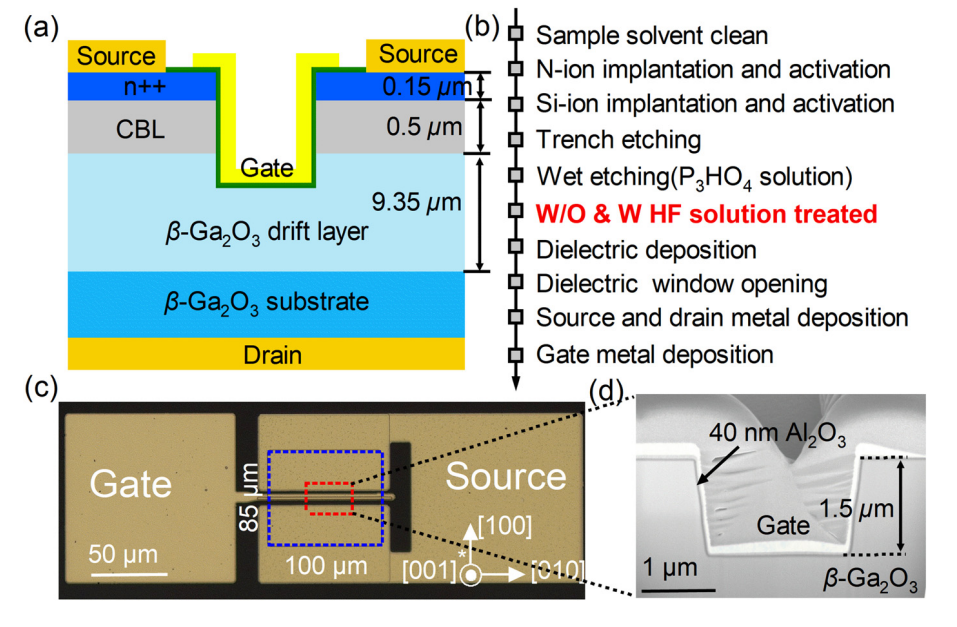
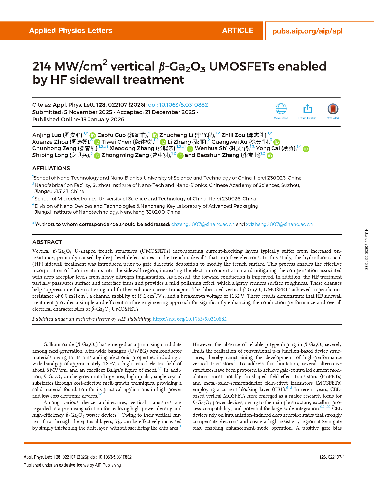
FIG. 1. (a) Schematic diagram of the β-Ga2O3 UMOSFET structure. (b) The β-Ga2O3 UMOSFET fabrication steps. (c) Optical microscope image of the β-Ga2O3 UMOSFET. (d) Cross-sectional scanning electron microscope (SEM) image of the β-Ga2O3 UMOSFET.
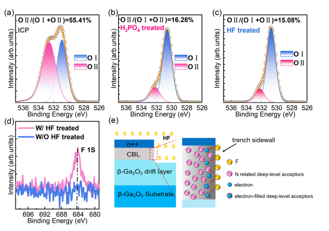
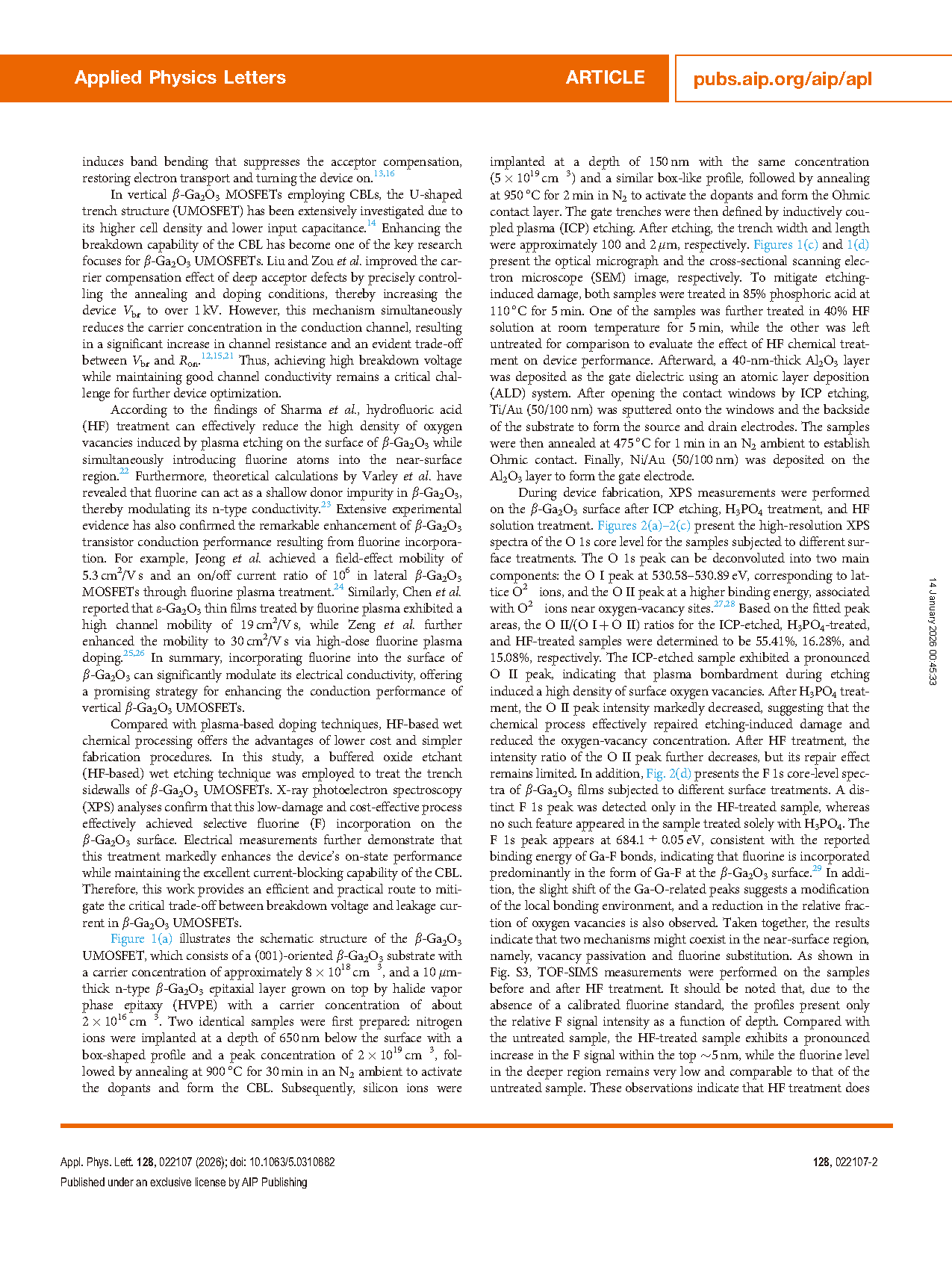
FIG. 2. The O 1s core-level XPS spectra of the β-Ga2O3 surfaces of (a) the ICP etching, and the treatment with (b) H3PO4 solution after etching and (c) HF solution after H3PO4 solution treatment. (d) The F 1s core-level XPS spectra of the β-Ga2O3 films subjected to different treatments. (e) Schematic illustration of the mechanism of HF treatment on the trench sidewall of β-Ga2O3 UMOSFETs.
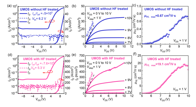
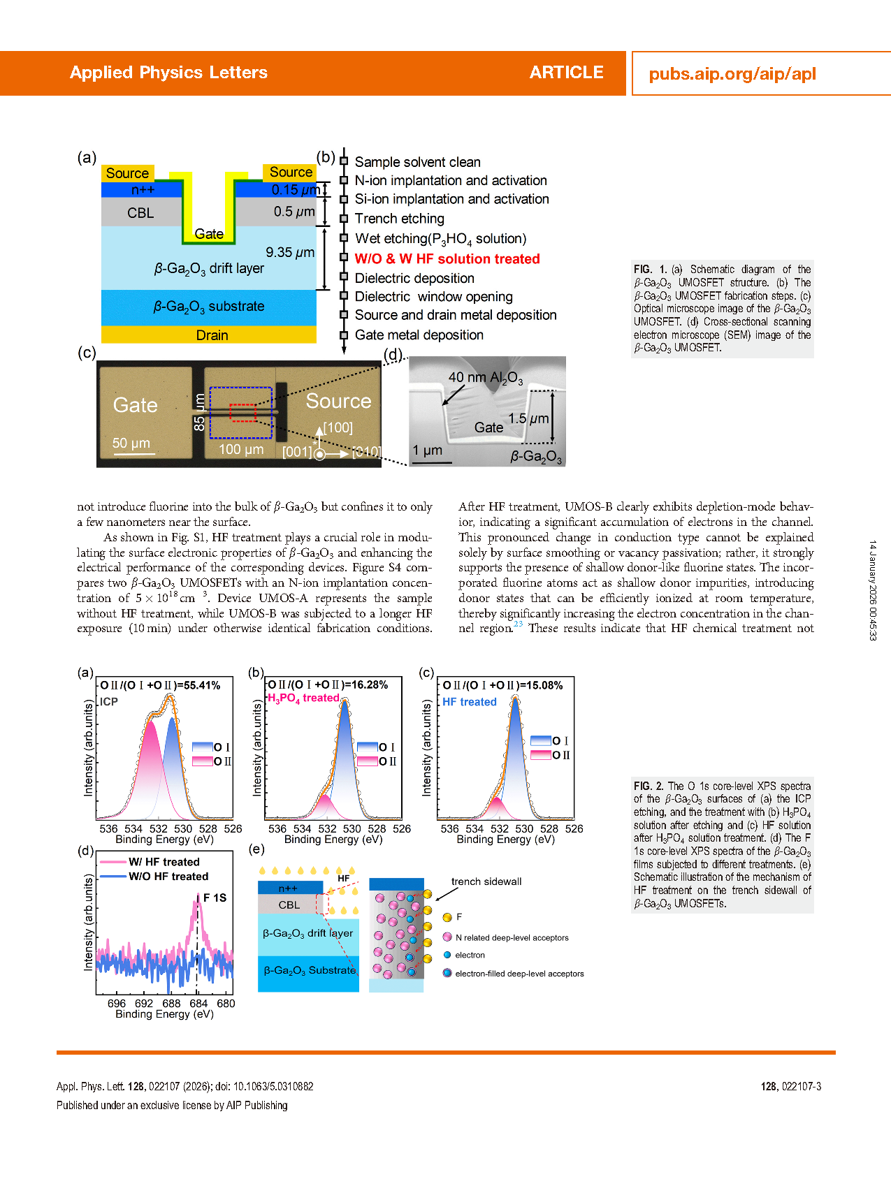
FIG. 3. Transfer characteristics of β-Ga2O3 UMOSFETs without (a) and with (d) HF solution treatment, presented on both linear and semilogarithmic scales. Comparison of the DC output characteristics of β-Ga2O3 UMOSFETs without (b) and with (e) HF treatment, plotted on a linear scale. Field-effect mobility (uFE) as a function of gate-to-source voltage (VGS) for β-Ga2O3 UMOSFETs without (c) and with (f) HF treatment.
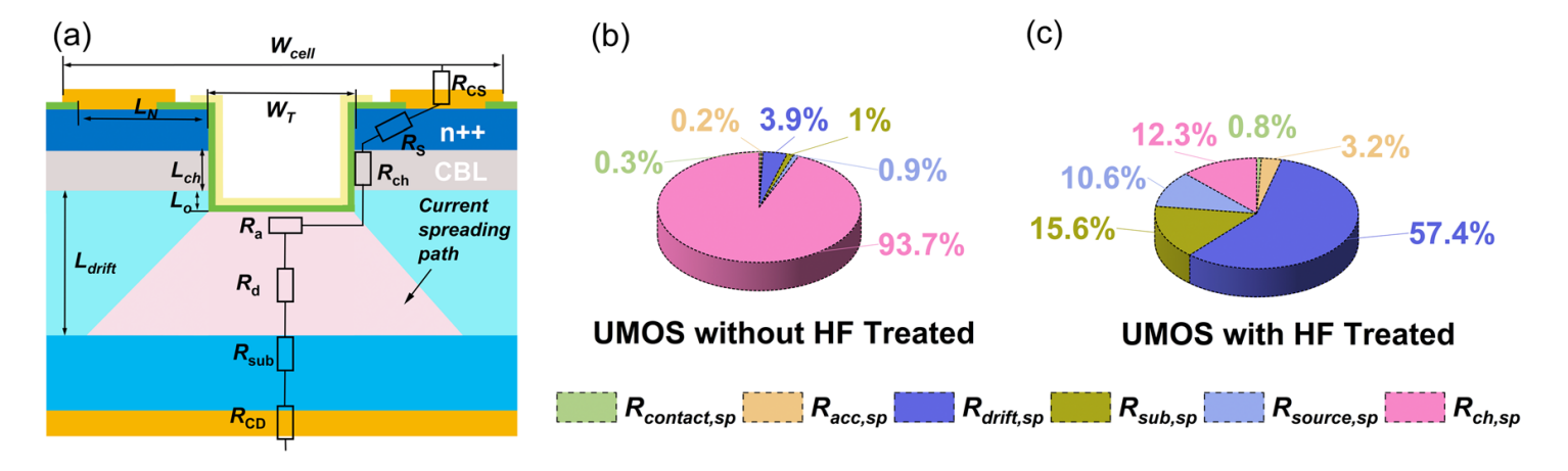
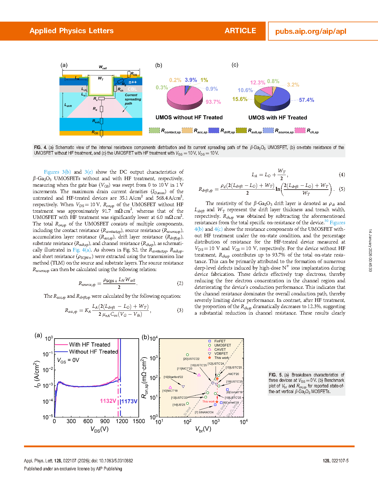
FIG. 4. (a) Schematic view of the internal resistance components distribution and its current spreading path of the β-Ga2O3 UMOSFET, (b) on-state resistance of the UMOSFET without HF treatment, and (c) the UMOSFET with HF treatment with VGS =10 V, VDS =10 V.
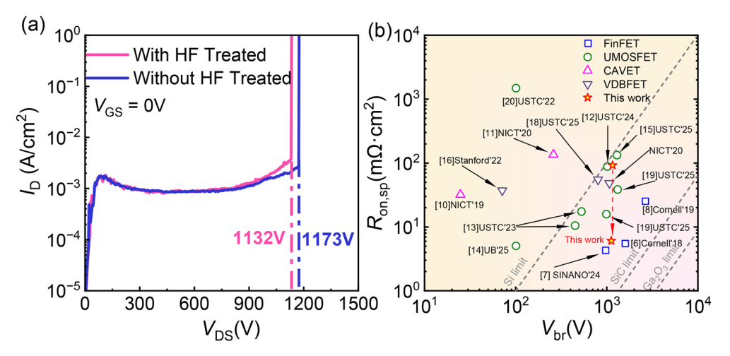
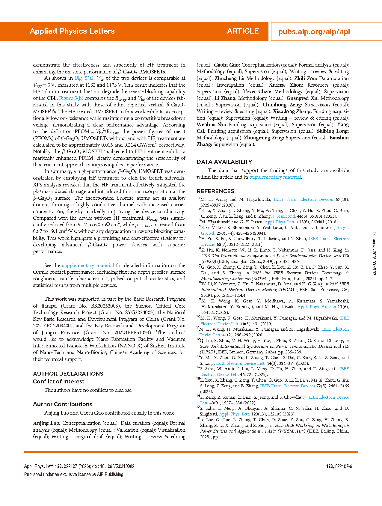
FIG. 5. (a) Breakdown characteristics of three devices at VGS = 0 V. (b) Benchmark plot of Vbr and Ron,sp for reported state-ofthe-art vertical β-Ga2O3 MOSFETs.
DOI:
doi.org/10.1063/5.0310882