Paper Sharing
【Domestic Papers】High-Temperature Enhancement-Mode Ga₂O₃ Monolithic Bidirectional Switch With >6.5 kV Breakdown Voltage
日期:2026-02-28阅读:400
Researchers from the Virginia Tech, Nanjing University and The University of Hong Kong have published a dissertation titled "High-Temperature Enhancement-Mode Ga2O3 Monolithic Bidirectional Switch With >6.5 kV Breakdown Voltage" in IEEE Electron Device Letters.
Background
Bidirectional switch (BDS), capable of blocking bipolar voltages in the off-state and conducting current in both directions in the on-state, are critical for AC power electronics applications. Conventional BDS implementations rely on two or four discrete devices in anti-series connection, which results in at least fourfold increase in chip area because each device contributes half of the total on-resistance. Monolithic BDS (MBDS) addresses this by using a single drift region, yielding chip areas comparable to unidirectional counterparts.
Over the past decade, extensive efforts have been devoted to developing MBDS based on SiC MOSFETs and GaN HEMTs. Lateral GaN HEMT-based MBDSs rated at 650 V are near market entry. While the advantage of MBDS over discrete implementations grows with breakdown voltage (BV), scaling BV remains challenging due to electric field (E-field) crowding. To date, the highest BV reported in GaN MBDSs is limited to 3.3 kV.
Abstract
This work demonstrates an enhancement-mode (E-mode) Ga2O3 monolithic bidirectional switch (MBDS) capable of high-temperature operation, achieving breakdown voltages (BV) exceeding 6.5 kV in both polarities at 150 °C and maintaining 4.7 kV at 200 °C. The device incorporates two highly doped NiO heterojunction gates, each connected to a lightly doped NiO junction termination extension (JTE) for electric field management. It exhibits symmetric conduction characteristics with a threshold voltage (VTH of 1.9 V and a specific on-resistance (Ron,sp) of 1755 mΩ·cm2. Even at 200 °C, VTH remains positive while Ron,sp increases by only 1.3×. This represents the best performance reported for ultra-wide bandgap (UWBG) E-mode MBDS devices and the first demonstration of a kilovolt MBDS operational up to 200 °C. These results suggest the potential of Ga2O3 MBDS for high-temperature, high-voltage applications.
Conclusion
This work demonstrates an E-mode Ga2O3 MBDS capable of high temperature operation. By optimizing the LJTE and tJTE of the NiO-based D-JTE, the BV achieves 6.5 kV in both polarities at 150 °C and maintains 4.7 kV at 200 °C. The NiO junction gate enables the E-mode operation that remains at 200 °C. As the first demonstration of a 200 °C-operational multi-kilovolt MBDS, these results suggest the good potential of Ga2O3 MBDS for high-voltage, high-temperature power electronics.
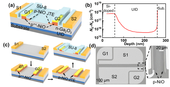
Fig. 1. (a) 3D schematic of Ga2O3 MBDS with p-NiO D-JTE. (b) The ND-NA depth profile of the Ga2O3 epilayers. (c) Key fabrication steps. (d) Top-view SEM image of the fabricated Ga2O3 MBDS.
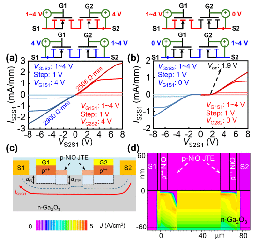
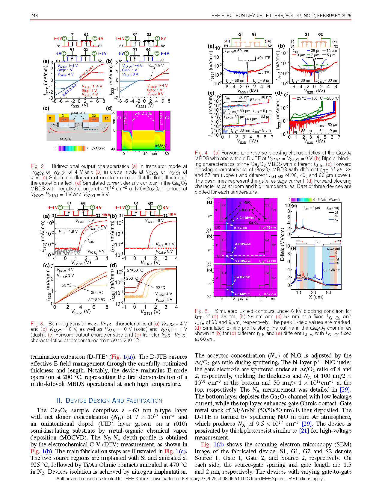
Fig. 2. Bidirectional output characteristics (a) in transistor mode at VG2S2 or VG1S1 of 4 V and (b) in diode mode at VG2S2 or VG1S1 of 0 V. (c) Schematic diagram of on-state current distribution, illustrating the depletion effect. (d) Simulated current density contour in the Ga2O3 MBDS with negative charge of ~1012 cm−2 at NiO/Ga2O3 interface at VG2S2 VG1S1 = 4 V and VS2S1 = 8 V.
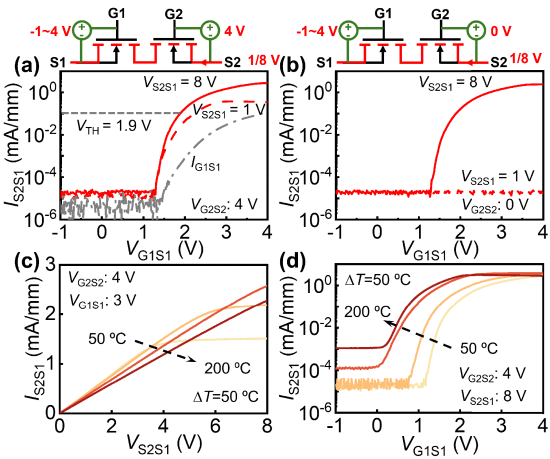
Fig. 3. Semi-log transfer IS2S1 -VG1S1 characteristics at (a) VG2S2 = 4 V and (b) VG2S2 = 0 V, as well as VS2S1 = 8 V (solid) and VS2S1 = 1 V (dash). (c) Forward output characteristics and (d) transfer IS2S1 -VG1S1 characteristics at temperatures from 50 to 200 °C.
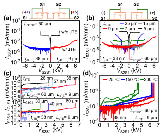
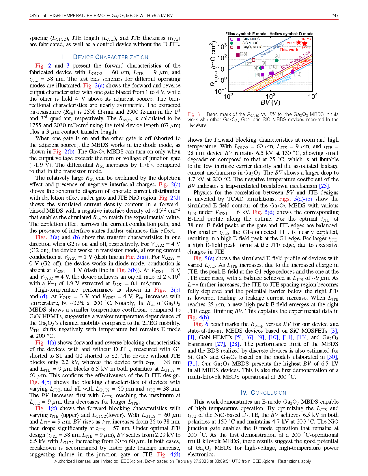
Fig. 4. (a) Forward and reverse blocking characteristics of the Ga2O3 MBDS with and without D-JTE at VG2S2=VG1S1= 0 V. (b) Bipolar blocking characteristics of the Ga2O3 MBDS with different LJTE. (c) Forward blocking characteristics of Ga2O3 MBDS with different tJTE of 26, 38 and 57 nm (upper) and different LG1 G2 of 30, 40, and 60 μm (lower). The dash lines represent the gate leakage current. (d) Forward blocking characteristics at room and high temperatures. Data of three devices are plotted for each temperature.
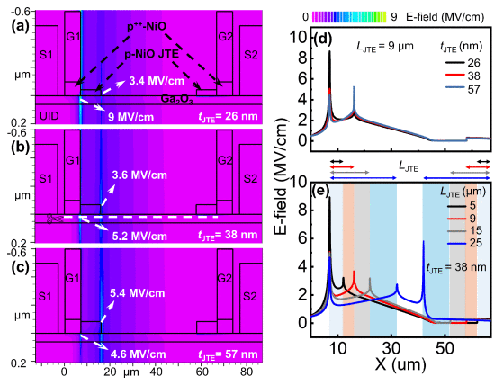
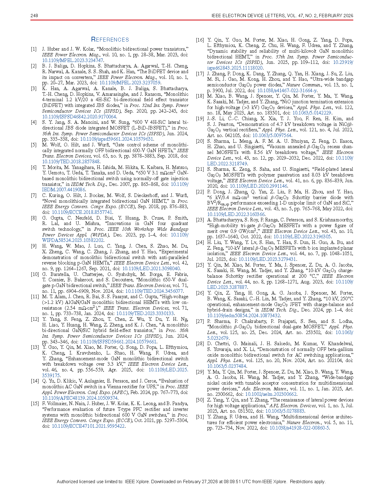
Fig. 5. Simulated E-field contours under 6 kV blocking condition for tJTE of (a) 26 nm, (b) 38 nm and (c) 57 nm at a fixed LG1 G2 and LJTE of 60 and 9 μm, respectively. The peak E-field values are marked. (d) Simulated E-field profile along the cutline in the Ga2O3 channel as shown in (b) for (d) different tJTE and (e) different LJTE , with LG1 G2 fixed at 60 μm.
Fig. 6. Benchmark of the Ron,sp vs. BV for the Ga2O3 MBDS in this work with other Ga2O3, GaN and SiC MBDS devices reported in the literature.
DOI:
doi.org/10.1109/LED.2025.3646042