Paper Sharing
【Domestic Papers】β-Ga₂O₃ diodes with ultra-high surge current enabled by Ag/AMB-AlN flip-chip packaging
日期:2026-03-02阅读:297
Researchers from the Beijing Microelectronics Technology Institute and Tsinghua University have published a dissertation titled "β-Ga2O3 diodes with ultra-high surge current enabled by Ag/AMB-AlN flip-chip packaging " in Journal of Electronic Science and Technology.
Background
The ultra-wide bandgap semiconductor, gallium oxide (Ga2O3), with its wide bandgap (4.5–4.9 eV), high critical electric field (6–8 MV/cm), high Baliga’s figure of merit (3000–4000) and low intrinsic carrier concentration is recognized as one of the most promising materials for the fourth-generation high-voltage power devices. However, its low thermal conductivity (approximately 1/6 that of silicon (Si)) leads to significant self-heating during operation, which severely limits the device performance.
Recent advancements in packaging, such as nano-silver paste, direct bond copper (DBC) substrates (achieving ∼2.8 K/W junction-to-case thermal resistance (Rth(J-C)) for Ga2O3 devices), and flip-chip structures, have improved thermal management. However, nano-silver paste faces electromigration failure under a high current density despite offering high thermal conductivity (>200 W/mK), and DBC substrates risk interfacial delamination at extreme temperatures (>250 °C). Moreover, solders (temperature-limited <220 °C) and copper substrates (coefficient of thermal expansion (CTE)-mismatch-induced stress) are used in traditional flip-chip solutions, which results in compromised reliability. Therefore, more innovative methods contributing to a further decrease in the thermal resistance while ensuring high reliability is still challenging. In this study, we demonstrate a low-Rth(J-C) solution via nano-silver thin-film hot-pressing on aluminum nitride active metal brazing (AMB-AlN) substrates with a flip-chip structure. Comprehensive reliability performance of different β-Ga2O3 devices, such as mesa-terminated Schottky barrier diodes (SBDs) and hetero-junction diodes (HJDs) with such advanced Ag/AMB-AlN flip-chip packaging, is evaluated including the high-temperature storage, reverse recovery, and surge current tests. The results provide key insights for Ga2O3 power device packaging.
Abstract
Owing to superior breakdown voltage and exceptional robustness, the β-Ga2O3 power device has emerged as a pivotal research frontier in power electronics. Although advanced packaging strategies, including nano-silver paste sintering, alumina direct bond copper (DBC) substrates, and flip-chip structures, have been adopted to mitigate β-Ga2O3’s intrinsic low thermal conductivity. However, a further reduction in the thermal resistance while maintaining high reliability remains a challenge. This study introduces a novel packaging methodology that synergistically integrates nano-silver films with aluminum nitride active metal brazing (AMB-AlN) substrates, achieving an ultra-low junction-to-case thermal resistance. Comprehensive reliability assessments were conducted on β-Ga2O3 Schottky barrier diodes (SBDs) and p-NiO/β-Ga2O3 hetero-junction diodes (HJDs), encompassing high-temperature storage test, reverse recovery analysis, and surge current characterization. The SBDs and HJDs exhibit surge current densities of ∼0.88 kA/cm2 and ∼0.78 kA/cm2, respectively, ranking among the highest reported levels for β-Ga2O3 power devices, which represents a significant advancement in device performance benchmarks. These advancements provide critical insights into packaging design for high-reliability ultra-wide bandgap semiconductor systems.
Conclusions
In this study, we packaged the β-Ga2O3 SBDs and HJDs with dimensions of . By utilizing a high-thermal-conductivity AMB substrate and a nano-scale silver sintering process to achieve low junction-to-case thermal resistance, the device reliability was evaluated. The results demonstrate that the β-Ga2O3 SBDs have excellent switching performance, featuring a reverse recovery time of 13.8 ns and a reverse recovery charge of 11.3 nC, highlighting their fast switching speed. Benefiting from their low turn-on voltage and optimized anode thermal design, the SBDs achieved a peak surge current density of ∼0.88 kA/cm2 under a 10 ms pulse width. In contrast, the β-Ga2O3 HJDs exhibited a superior breakdown voltage, lower reverse leakage current, and exceptional high-temperature stability, with negligible performance degradation during HTST at 250 °C. This work underscores the excellent robustness of β-Ga2O3 diodes and provides theoretical guidance for selecting devices tailored to different operational environments.
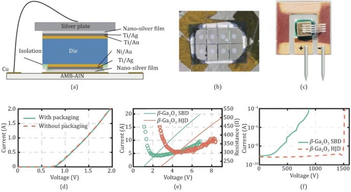
Fig. 1. Structural and electrical characterization of packaged β-Ga2O3 devices: (a) cross section of die with the flip-chip packaging structure, (b) photograph of the chip with a Ti/Ag layer, (c) photograph of a packaged device, (d) forward I-V characteristics of devices with or without packaging, and (e) forward I-V (solid lines) and R-V (point curves) characteristics and (f) reverse I-V characteristics of the packaged β-Ga2O3 SBD and HJD devices.
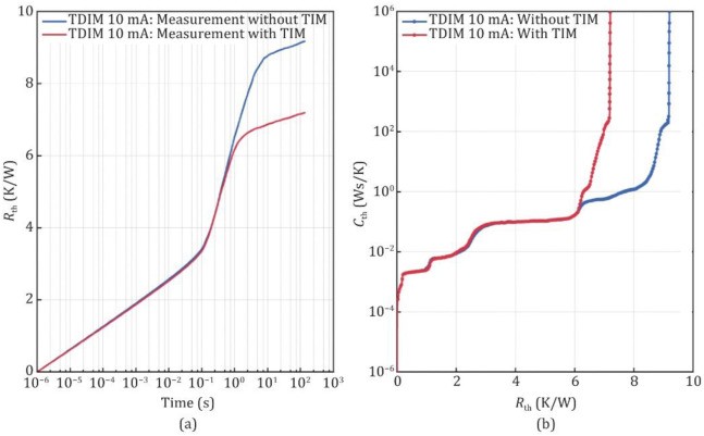
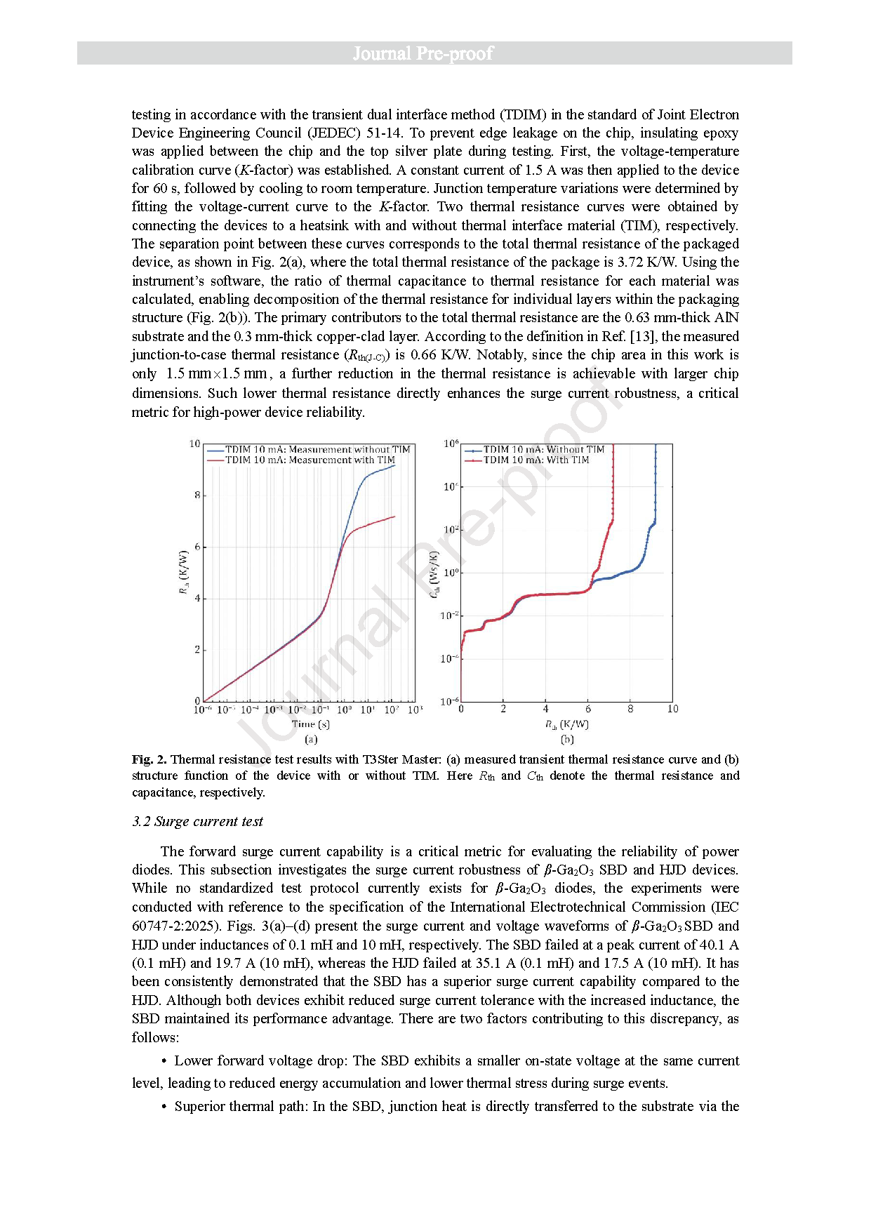
Fig. 2. Thermal resistance test results with T3Ster Master: (a) measured transient thermal resistance curve and (b) structure function of the device with or without TIM. Here Rth and Cth denote the thermal resistance and capacitance, respectively.
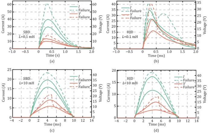
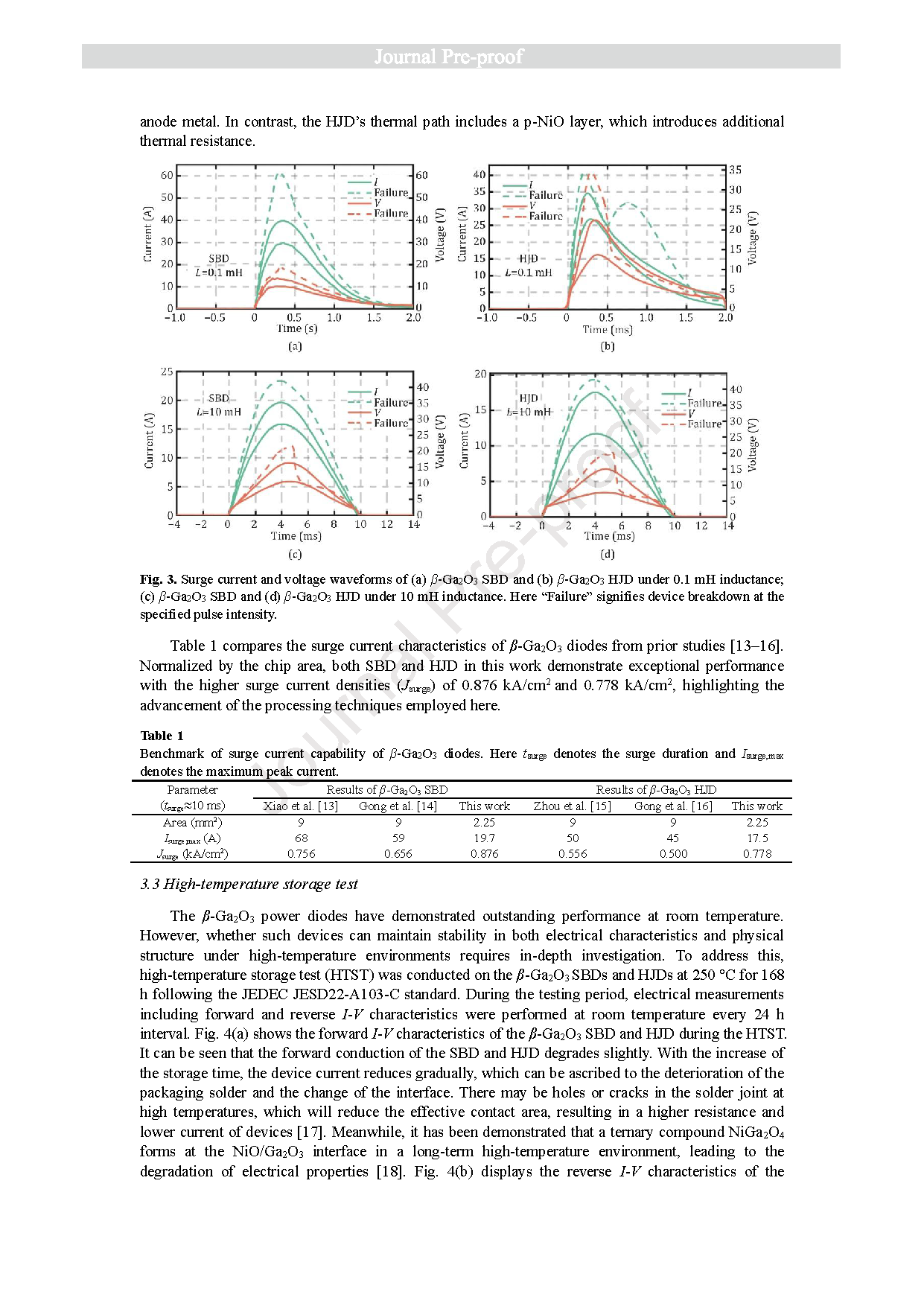
Fig. 3. Surge current and voltage waveforms of (a) β-Ga2O3 SBD and (b) β-Ga2O3 HJD under 0.1 mH inductance; (c) β-Ga2O3 SBD and (d) β-Ga2O3 HJD under 10 mH inductance. Here “Failure” signifies device breakdown at the specified pulse intensity.
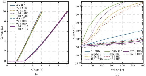
Fig. 4. Results of HTST: (a) forward and (b) reverse I-V characteristics of the β-Ga2O3 SBD and HJD before and after HTST.
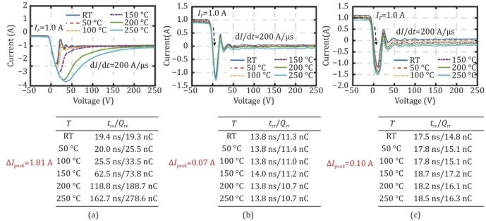
Fig. 5. Reverse recovery characteristics of (a) Si FRD, (b) β-Ga2O3 SBD, and (c) β-Ga2O3HJD at different temperatures. The table shows the trr and Qrr of the diode at different temperatures (T). Here RT denotes the room temperature and ΔIpeak denotes the difference in current peaks across temperatures.
DOI:
doi.org/10.1016/j.jnlest.2026.100347