Paper Sharing
【Domestic Papers】Pt Nanoparticle–Decorated β-Ga₂O₃/n-GaN Solar–Blind UV photodetectors with enhanced photoresponse for reconfigurable optoelectronic logic gates
日期:2026-03-03阅读:305
Researchers from the Guangdong University of Technology have published a dissertation titled "Pt Nanoparticle–Decorated β-Ga2O3/n-GaN Solar–Blind UV photodetectors with enhanced photoresponse for reconfigurable optoelectronic logic gates" in Optics & Laser Technology.
Project Support
This work was financially supported by the Open Research Fund of Songshan Lake Materials Laboratory [grant numbers 2023SLABFK01]; Guangzhou Science and Technology Program (No. 2025A04J3852); National Natural Science Foundation of China [grant numbers 62004229].
Background
Solar radiation with wavelengths shorter than 280 nm is strongly absorbed by the atmospheric ozone layer and is thus unable to reach the Earth’s surface, creating to the so-called “solar-blind ultraviolet” (SBUV) band. Imaging or detection within this band benefits from zero solar background, extremely low noise, and therefore a high signal-to-noise ratio, low false-alarm rate and unambiguous target recognition. Consequently, SBUV detection technology is attractive for environmental monitoring, missile tracking, flame detection, and near-ground communication. SBUV photodetectors, which convert incident SBUV radiation into electrical signals, are the core component of SBUV photodetection technology. Their performance critically determines the reliability of SBUV photodetection systems. Therefore, the selection of appropriate core materials that enable the fabrication of high-performance detectors is essential. Wide-bandgap semiconductors, such as gallium oxide (Ga2O3), have emerged as ideal candidates for the fabrication of SBUV photodetectors due to their ultra-wide bandgap, thermodynamic and chemical stability, strong anti-interference capability, and high critical electric field.
Abstract
In this work, β-Ga2O3/n-GaN heterojunctions modified with Pt nanoparticles (NPs) are fabricated via an in-situ thermal oxidation process. The performance of the resulting solar-blind ultraviolet (SBUV) photodetectors is enhanced by the localized surface plasmon resonance (LSPR) effect of the Pt NPs. Under zero bias and 254 nm illumination, the device decorated with a high proportion (≥90.4%) of small-sized (diameter ≤ 80 nm) Pt NPs exhibits a higher responsivity (3.2 mA W⁻1) and a larger D* (8.7 × 10¹⁰ Jones) compare to the device without Pt NPs. As the proportion of larger-sized (> 80 nm) Pt NPs increases, charge redistribution is induced at the Pt/β-Ga2O3 interface, which strengthens the defect-related persistent photoconductivity (PPC) effect and switches the device operation from photovoltaic to photoconductive mode. Furthermore, the LSPR-enhanced β-Ga2O3/n-GaN heterojunction device realizes reconfigurable optoelectronic logic operations, including NOT, NAND, NOR, AND, and OR logic operations. This study provides an efficient approach for SBUV optoelectronic logic systems and lays the foundation for the development of low-power and highly integrated SBUV computing chips, showing great potential for advancing encrypted optical communication, multispectral imaging, and bioinspired sensing.
Highlights
● Ga2O3/GaN heterojunctions with Pt NPs form in situ via one-step thermal oxidation.
● LSPR effect of Pt NPs boosts the heterojunction photodetector’s performance.
● Operational mode switching of the device is achieved via Pt NPs size tuning.
● Five optoelectronic logic gates are realized within a Ga2O3/GaN device.
Conclusion
In summary, Pt NPs-modified β-Ga2O3/n-GaN heterojunctions are constructed by direct high-temperature annealing of GaN substrates pre-deposited with Pt thin films, thereby fabricating high-performance Pt/β-Ga2O3/n-GaN SBUV photodetectors. Compared with the device without Pt NPs modification, the Pt NPs-modified devices exhibit higher responsivity, EQE and D* under zero bias and SBUV illumination. The enhanced performance in photovoltaic mode is attributed to the LSPR induced by Pt NPs. As the proportion of large-sized Pt NPs modified at the Pt/β-Ga2O3 interface increases, the defect-related PPC effect at the Pt/β-Ga2O3 interface is enhanced, leading to a transition in the device operation mode from photovoltaic to photoconductive. The ability to control the device's operation mode through Pt NPs size, particularly the efficient photovoltaic mode enabled by small NPs, provides a critical foundation for designing advanced optoelectronic circuits. By leveraging this LSPR-enhanced effect under photovoltaic mode, the heterojunction devices successfully demonstrate five types of reconfigurable optoelectronic logic gate functions (NOT, NAND, NOR, AND, OR). These demonstrations highlight the potential of this work for next-generation SBUV photonic systems and computing, with promising applications in encrypted communication, multispectral imaging, and bioinspired vision.
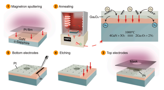
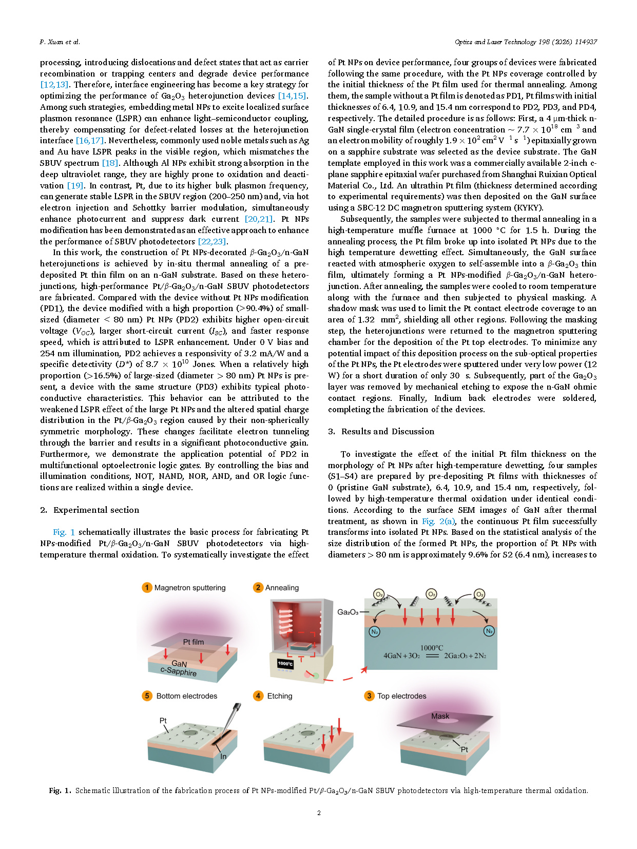
Fig. 1. Schematic illustration of the fabrication process of Pt NPs-modified Pt/β-Ga2O3/n-GaN SBUV photodetectors via high-temperature thermal oxidation.
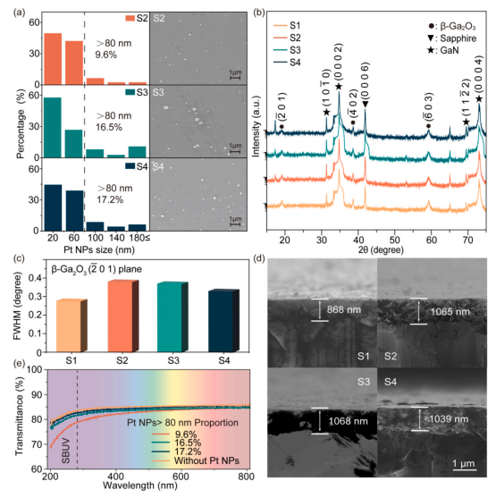
Fig. 2. (a) SEM morphology of Pt NPs in different samples and their corresponding size distribution statistics, (b) XRD patterns of different samples, (c) comparison of the full width at half maximum (FWHM) of the (–2 0 1) crystal plane of the β-Ga2O3 layer in different samples, and (d) cross-sectional SEM images of different samples. The four samples labeled S1, S2, S3, and S4 correspond to those thermally oxidized after the deposition of initial Pt films with thicknesses of 0 (Pt film-free), 6.4, 10.9, and 15.4 nm on GaN substrates, respectively. (e) Comparison of transmission spectra of a sapphire substrate without Pt NPs modification and sapphire substrates with different Pt NPs coverages (proportions of particles > 80 nm: 9.6%, 16.5%, and 17.2%).

Fig. 3. Comparison of the optoelectronic performance of PD1, PD2, PD3, and PD4. I–V curves of these devices under dark conditions (a) and under 254 nm illumination with an optical power of 4.9 μW (b). Dependence of the photo-to-dark current ratio (PDCR) (c) and the SBUV to UV rejection ratio (R254/R365) (d) on voltage. Schematic energy band diagrams of β-Ga2O3/n-GaN heterojunctions modified with small-sized Pt NPs (e) and large-sized Pt NPs (f) under SBUV illumination.
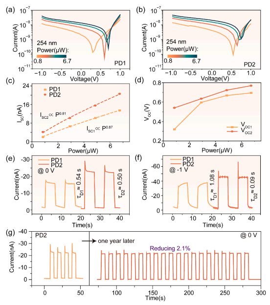
Fig. 4. Optoelectronic performance comparison between PD1 and PD2 devices: Power-dependent I–V characteristics for (a) PD1 and (b) PD2. (c) Variation of ISC with light intensity for the devices, along with their respective fitting factors. (d) Variation of VOC with light intensity for the devices. I–t curves of the devices under 6.7 μW 254 nm illumination and at 0 V bias (e) and –1 V bias (f), respectively. (g) Stability and reproducibility of PD2 photocurrent at 0 V bias under periodic 254 nm with 6.7 μW illumination.
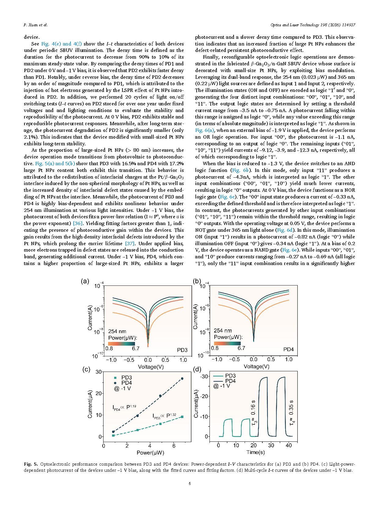
Fig. 5. Optoelectronic performance comparison between PD3 and PD4 devices: Power-dependent I–V characteristics for (a) PD3 and (b) PD4. (c) Light-power-dependent photocurrent of the devices under –1 V bias, along with the fitted curves and fitting factors. (d) Multi-cycle I–t curves of the devices under –1 V bias.
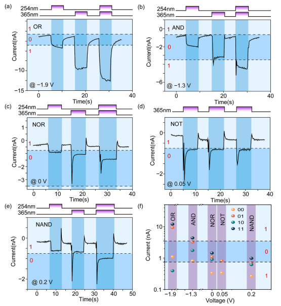
Fig. 6. Reconfigurable optoelectronic logic operations based on the Pt NP-modified β‑Ga2O3/n-GaN heterojunction device. Demonstration of five fundamental logic gates: (a) NOR, (b) NAND, (c) NOT, (d) AND, and (e) OR. (f) Summary truth table of the steady-state photocurrent outputs for the five optical logic gates. The original steady-state currents are all negative. Therefore, the ranges of currents and threshold intervals on the vertical axis are expressed in absolute value.
DOI:
doi.org/10.1016/j.optlastec.2026.114937