Paper Sharing
【Member Papers】Space-charge-limited effect on the temperature-dependent performance of Fe-doped β-Ga₂O₃ x-ray detector
日期:2026-03-06阅读:298
Researchers from the Xi'an Jiaotong University have published a dissertation titled "Space-charge-limited effect on the temperature-dependent performance of Fe-doped β-Ga2O3 x-ray detector" in Applied Physics Letters.
Project Support
This work was supported by the National Natural Science Foundation of China, Grant Nos. 12575199 and 62204198, and the Steady Support Fund for National Key Laboratory, Grant No. JBSY252800260. The authors thank Mr. Mingchao Yang in the School of Microelectronics, Xi’an Jiaotong University, for his invaluable assistance with fabrication support.
Background
Beta-gallium oxide (β-Ga2O3) has emerged as a research hotspot in x-ray detector technology due to its high breakdown electric field, excellent radiation resistance, high-temperature tolerance, and low-cost preparation methods. However, due to the presence of intrinsic defects (such as Si, Ge, and Sn) and shallow donor impurities, the unintentional-doped (UID) β-Ga2O3 typically exhibits n-type conductivity with high conductivity. This leads to a considerable leakage (dark) current at high bias voltages, limiting the charge collection efficiency of the detector. Typically, high-resistivity bulk Ga2O3 materials are achieved by doping Mg or Fe into the β-Ga2O3 crystal, as these elements can occupy Ga lattice sites and serve as acceptors to compensate for free electrons. Therefore, high-resistivity β-Ga2O3-based devices can generally be used for radiation detection and exhibit a fast pulse response after reducing dark current, giving them an advantage in direct conversion x-ray detection. However, the presence of additional defects and traps in the material is notable. Studies on x-ray detectors based on high-resistivity monocrystals suggested that not only did the charge collection process degrade but the response mechanisms were also highly susceptible to trap interactions. Unlike shallow-level traps, deep-level traps resulting from self-compensation exhibited distinct behaviors at elevated temperatures. Nonetheless, investigations into how these traps affect the high-temperature characteristics of devices remain limited.
Conclusion
In short, a vertical MSM x-ray detector based on compensated Fe-doped β-Ga2O3 was fabricated and systematically evaluated for its conduction and temperature-dependent response. Fe doping effectively suppressed the dark current by compensating native donors and introducing deep-level traps. These traps facilitated the formation of space charge by restricting injected carriers, resulting in multistage SCLC behavior at room temperature, which transitioned from ohmic conduction to trap-filled limited conduction and ultimately to trap-free SCLC. Under x-ray illumination, the illumination-generated nonequilibrium carriers were continuously regulated by traps, leading to the formation of space charge, which caused the net output current to follow the SCLP mechanism. However, the internal electric field induced by the accumulated space charge partially shielded the applied bias, reducing carrier collection. Since traps and multiple carrier types were involved in the transport process, temperature changes inevitably affected the balance among these factors, thereby altering the conductive mechanism and performance. Therefore, temperature-dependent tests were conducted to analyze this pattern of variation. As the temperature increased from 300 to 400 K, the net photocurrent initially decreased due to the enhanced trap-induced space charge, then increased as the trapped carriers were thermally released. At 450 K, thermally activated carriers began to dominate the transport process, suppressing the SCLC regime and causing a surge in the dark current that overwhelmed the response signal. Overall, charge transport in the compensated Fe-doped β-Ga2O3 detector is governed by the interplay between trap compensation, space-charge accumulation, and thermal activation, underscoring the importance of optimizing operating temperature to maximize high-temperature detection performance.
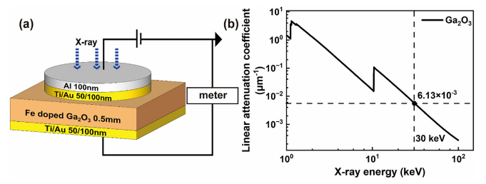
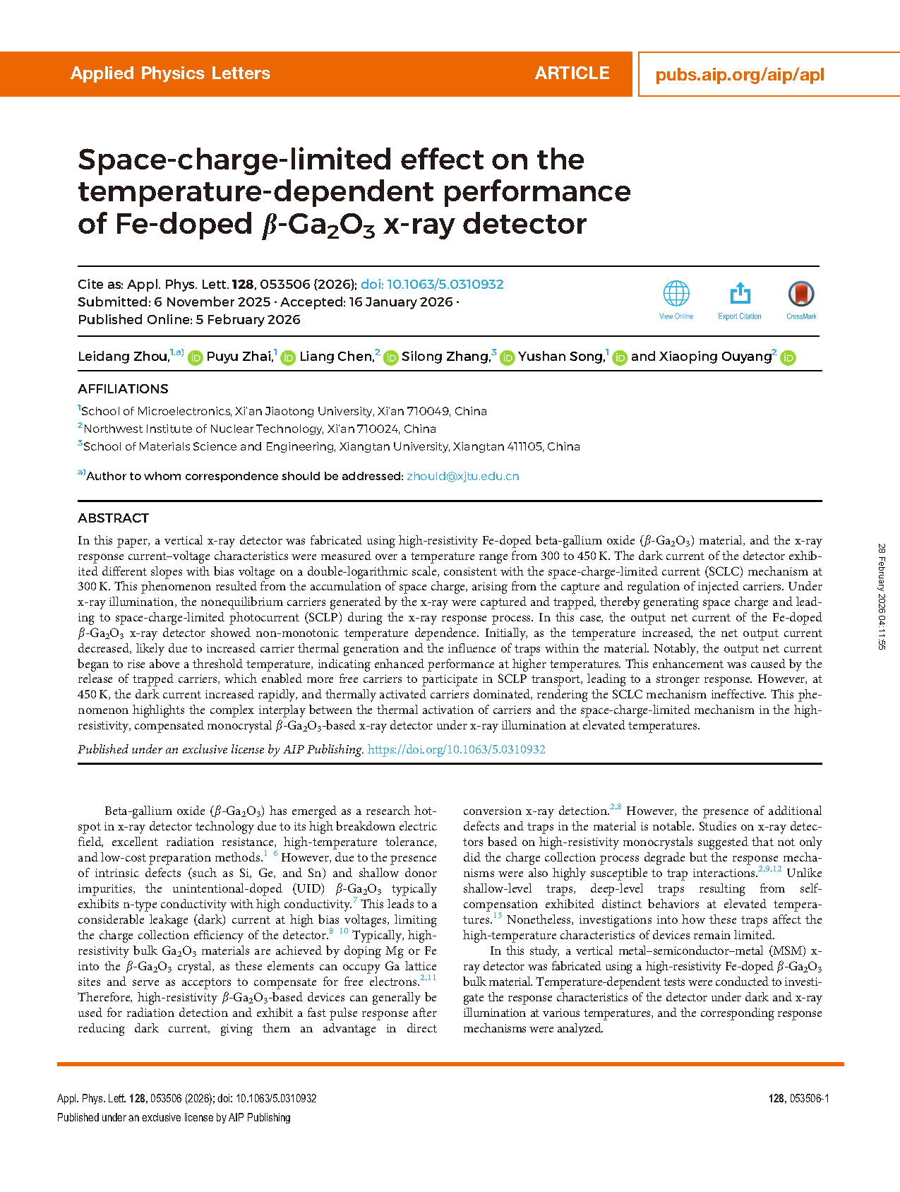
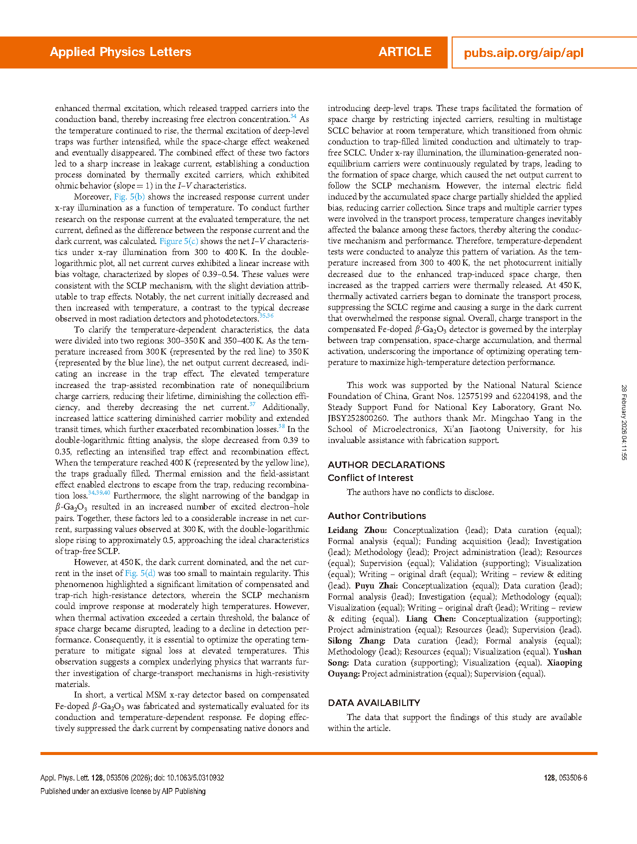
FIG. 1. (a) Schematic diagram of the vertical MSM detector based on the high-resistivity Fe-doped β-Ga2O3 bulk. (b) Linear attenuation coefficient diagram of Ga2O3 material for various x-ray photon energies.
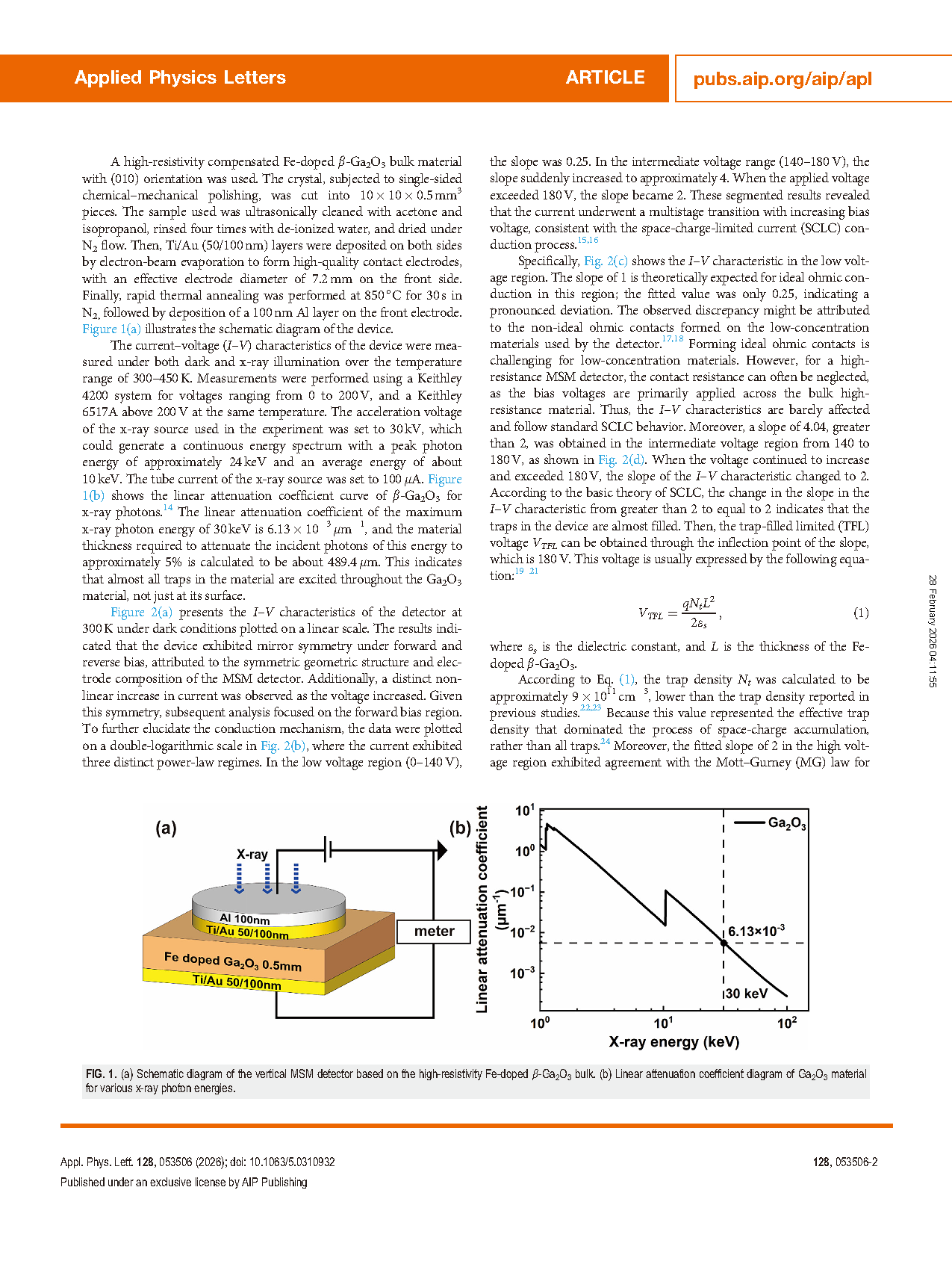
FIG. 2. (a) I–V characteristic curve of detector at 300 K under dark conditions (linear scale). (b) Forward I–V characteristic and linear fitting curve (double-logarithmic scale) of the detector at 300 K under dark conditions. (c) I–V characteristic of the low voltage region. (d) I–V characteristic of the intermediate voltage region. (e) I–V characteristic of the high voltage region.
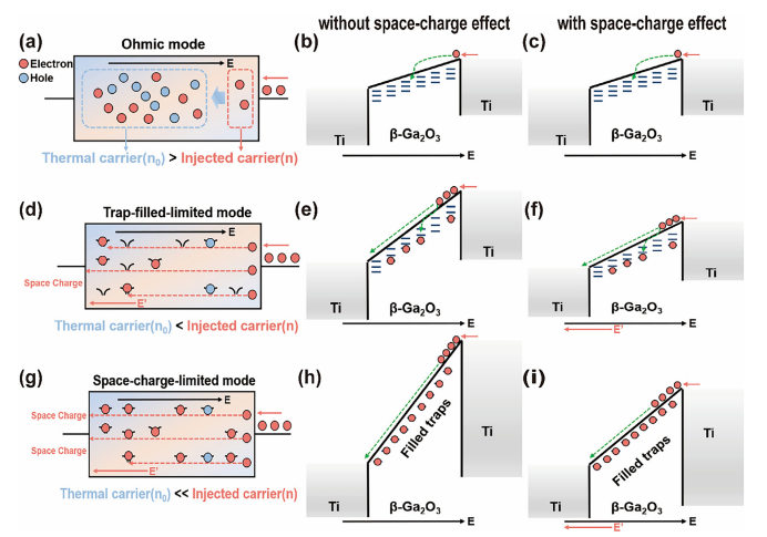
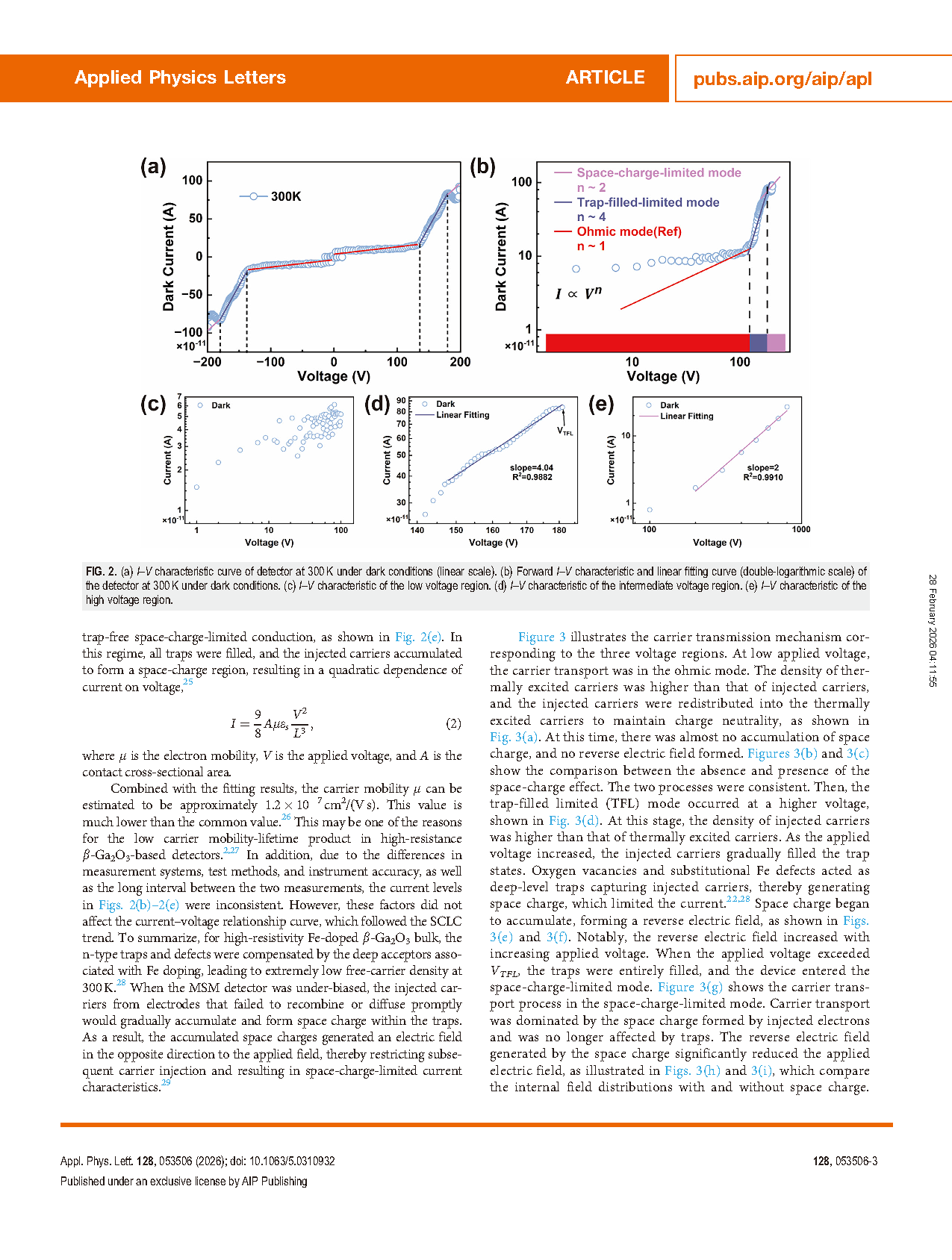
FIG. 3. (a)–(c) Schematic diagram of carrier transport in ohmic mode within the MSM structure. (d)–(f) Schematic diagram of carrier transport in trap-filled limited mode within the MSM structure. (g)–(i) Schematic diagram of carrier transport in space-charge-limited mode within the MSM structure.
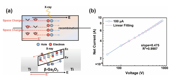
FIG. 4. (a) Schematic diagram of carrier transport in SCLP mode within the MSM structure. (b) Net I–V characteristic under x-ray illumination and its linear fitting curve.
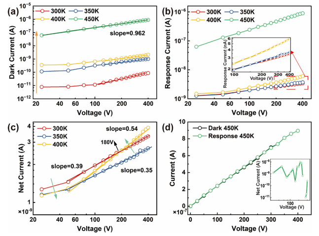
FIG. 5. (a) Dark I–V characteristics and (b) response I–V characteristics under x-ray illumination within the temperature range of 300–450 K. (c) Net I–V characteristics under x-ray illumination within the temperature range of 300–400 K. (d) Dark current, response current, and net current curves at 450 K.
DOI:
doi.org/10.1063/5.0310932