Paper Sharing
【Member Papers】Structural and electrical characterization of homoepitaxial (-102) β-Ga₂O₃ layers grown by halide vapor phase epitaxy using synchrotron x-ray topography and emission microscopy
日期:2026-03-10阅读:264
Researchers from the Novel Crystal Technology, Inc. have published a dissertation titled "Structural and electrical characterization of homoepitaxial (-102) β-Ga2O3 layers grown by halide vapor phase epitaxy using synchrotron x-ray topography and emission microscopy" in Applied Physics Letters.
Background
Beta-gallium oxide (β-Ga2O3) is an emerging ultra-wide bandgap (UWBG) semiconductor characterized by a bandgap of approximately 4.8 eV and a high critical electric field strength of 8MV/cm, both of which are higher than those of SiC and GaN. An additional significant advantage of β-Ga2O3 is that its single crystal can be achieved by melt growth, which enables large-scale production of high-quality material at low cost. Various melt-growth methods have been employed to synthesize β-Ga2O3 single crystals, including edge-defined film-fed growth (EFG), floating zone (FZ), Czochralski (CZ), and vertical Bridgman (VB) techniques.7–11 Among these methods, EFG has been adopted for industrial-scale production due to its high crystal quality and high growth rate. As a result, (001)-oriented β-Ga2O3 EFG substrates with diameters up to 4 in. are already commercially available. These merits have accelerated the development and research of β-Ga2O3-based devices. To date, besides (001)-oriented β-Ga2O3 substrates, (-102)-oriented substrates have also attracted considerable attention as a promising alternative due to the following advantages: Large-size (-102) substrates can be achieved using the EFG method similar to that established for (001) substrates. They also demonstrate a higher polishing rate, resulting in ease of wafer processing. Moreover, (-102) β-Ga2O3 substrates enable smooth (100)-sidewalls, making them suitable for the fabrication of vertical fins and trench applications. However, the suitability of this orientation for practical device applications, as well as the influence of crystal defects in the (-102) β-Ga2O3 epitaxial layer on device performance, is yet to be thoroughly investigated. Therefore, this work provides a comprehensive study of the (-102) wafer, covering substrate and epitaxial evaluation, SBD characterization, and the identification of killer defects.
Abstract
This study demonstrates that (-102) β-Ga2O3 is a promising candidate for homoepitaxial growth via halide vapor phase epitaxy. Synchrotron x-ray rocking curve measurements confirmed a uniform full-width at half-maximum of approximately 16 arc sec across the wafer for both the substrate and the epitaxial layer. A donor concentration in the range from 7 × 10¹⁵ to 1 × 1016 cm−3 was confirmed by capacitance–voltage measurements of the Schottky barrier diodes (SBDs). Among the 35 SBDs, 32 exhibited a leakage current density lower than the detection limit under a reverse bias of −300 V, resulting in a high yield of approximately 91%. Synchrotron x-ray topography observation further identified that residual polycrystalline defects within the epitaxial film, which persist even after chemical mechanical polishing, were responsible for the reverse leakage current of the SBDs.
Conclusion
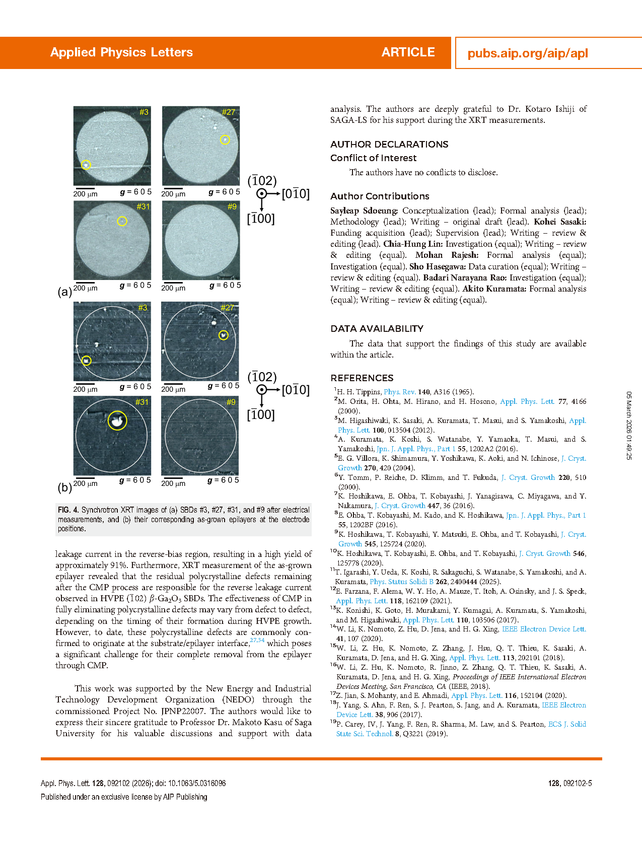
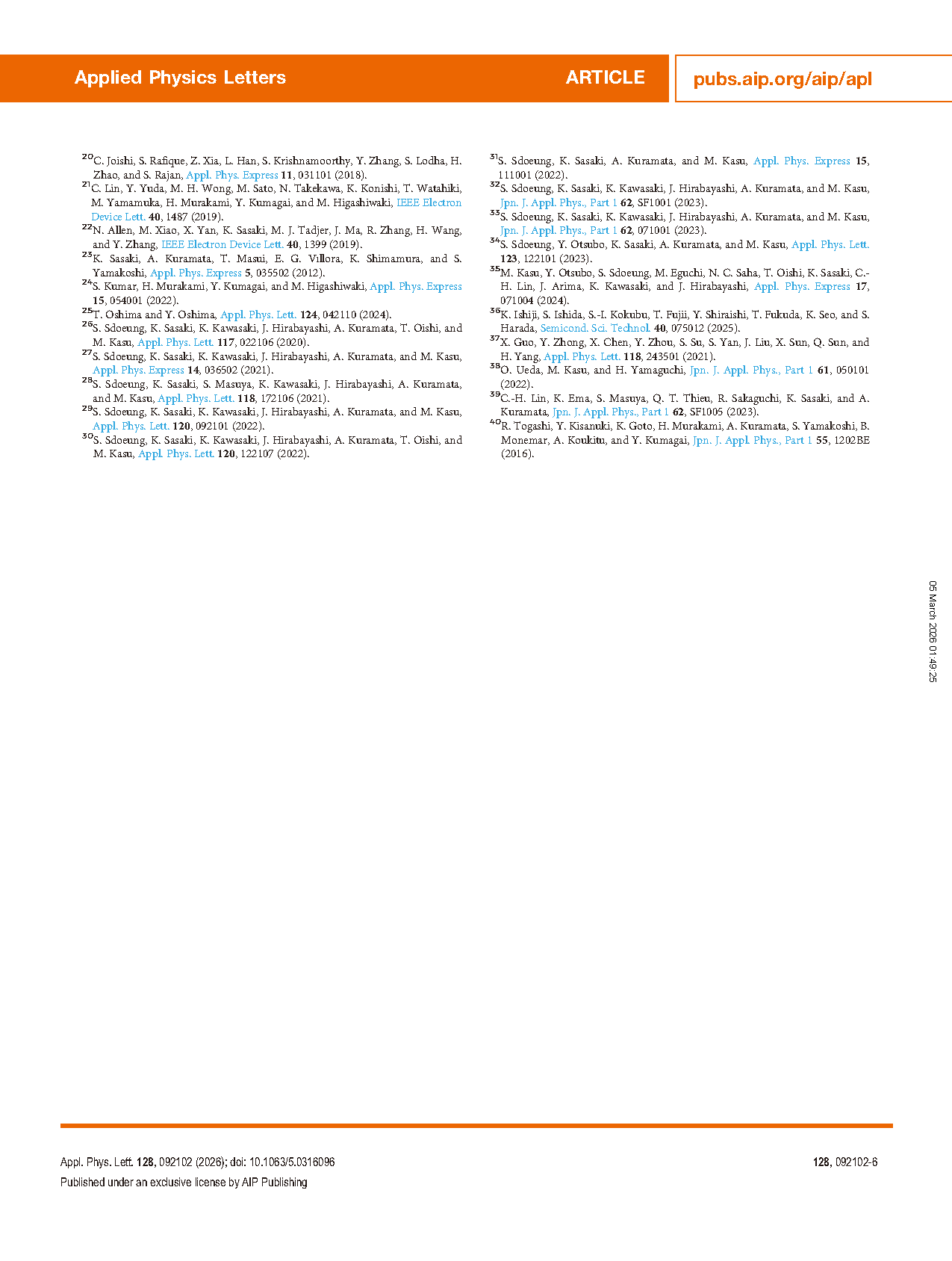
In conclusion, we confirmed that (-102) β-Ga2O3 is a promising candidate for HVPE homoepitaxial growth. Synchrotron XRC measurements confirmed a uniform FWHM of approximately 16 arc sec across the wafer for both the substrate and the epitaxial layer, indicating high crystallinity and showing no significant degradation of crystal quality occurred during HVPE growth. Additionally, C-V measurements of the SBDs revealed a donor concentration ranging from 7 × 10¹⁵ to 1 × 1016 cm−3. Among the 35 SBDs, three exhibited high leakage current in the reverse-bias region, resulting in a high yield of approximately 91%. Furthermore, XRT measurement of the as-grown epilayer revealed that the residual polycrystalline defects remaining after the CMP process are responsible for the reverse leakage current observed in HVPE (-102) β-Ga2O3 SBDs. The effectiveness of CMP in fully eliminating polycrystalline defects may vary from defect to defect, depending on the timing of their formation during HVPE growth. However, to date, these polycrystalline defects are commonly confirmed to originate at the substrate/epilayer interface, which poses a significant challenge for their complete removal from the epilayer through CMP.
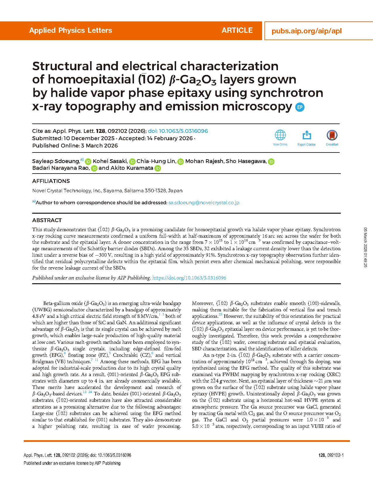
FIG. 1. Synchrotron XRC FWHM mapping images of (a) the substrate and (b) the HVPE layer (after CMP) taken by g vector of 2 -2 4. The yellow arrows highlight the FWHM values at corresponding locations in the substrate and epilayer. XRT images of the red-outlined regions of #1 and #2 were obtained using g vector = 6 0 5 in reflection geometry.
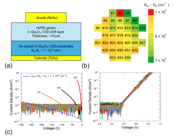
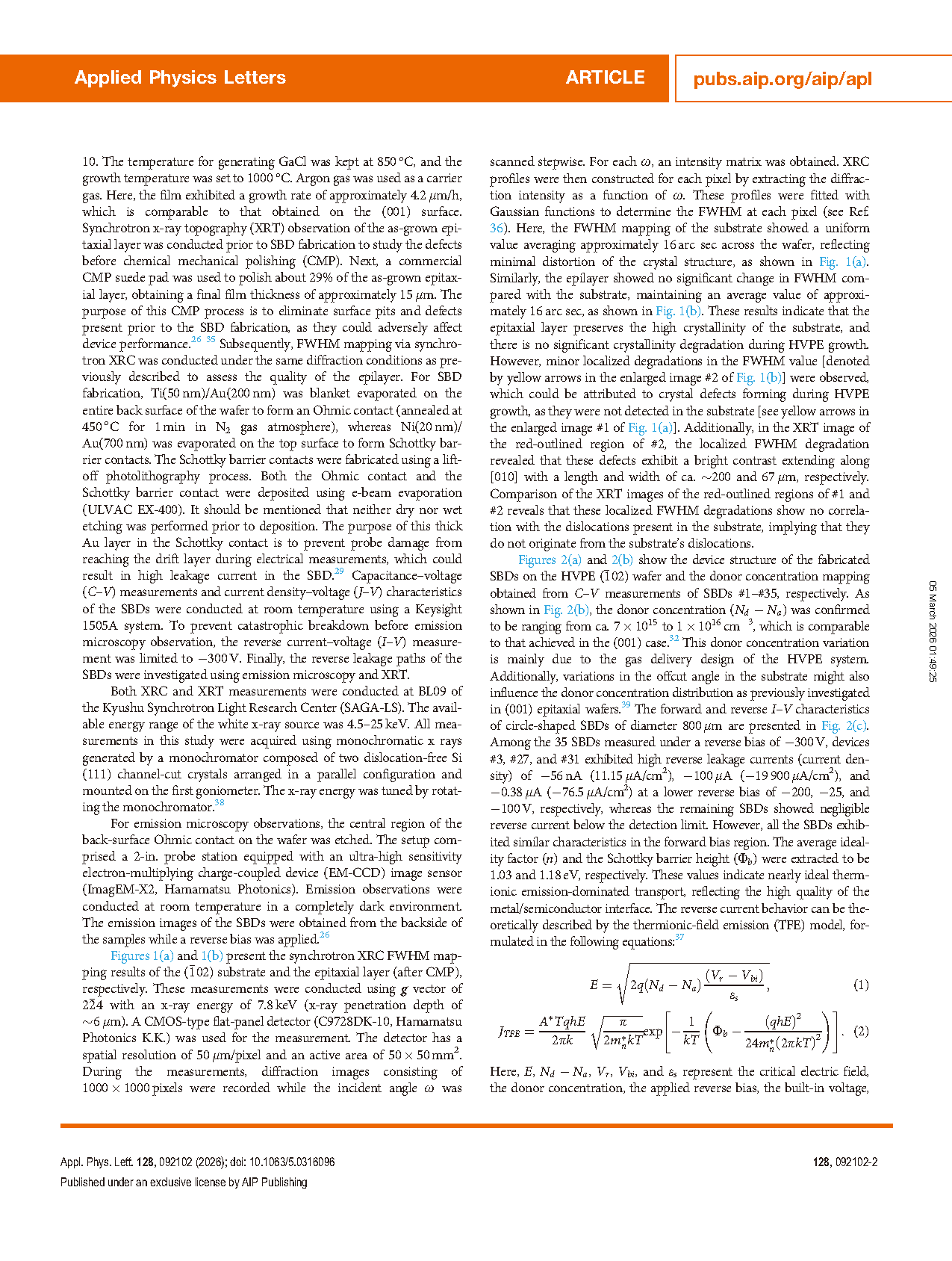
FIG. 2. (a) Cross-sectional view of the HVPE (-102) β-Ga2O3 SBD’s structure, (b) donor concentration mapping obtained by C–V measurements, and (c) J–V characteristics of the 800-μm-diameter SBDs, respectively. The blue-dashed line in the reverse-bias region represents the fitted curve based on the TFE model.
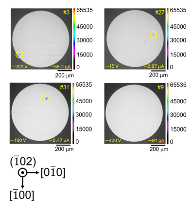
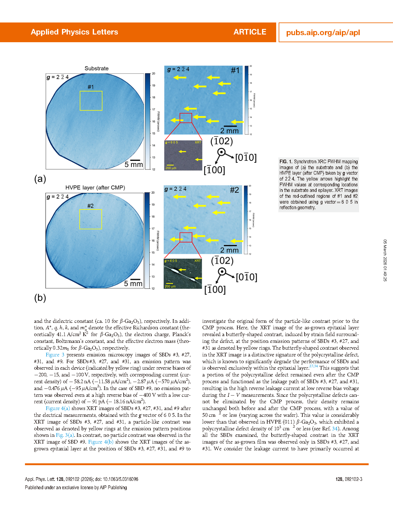
FIG. 3. Emission microscopy images of SBDs #3, #27, #31, and #9 under the reveres bias of 200, 15, 100, and 400 V, respectively.
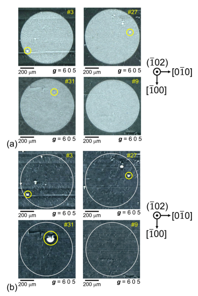
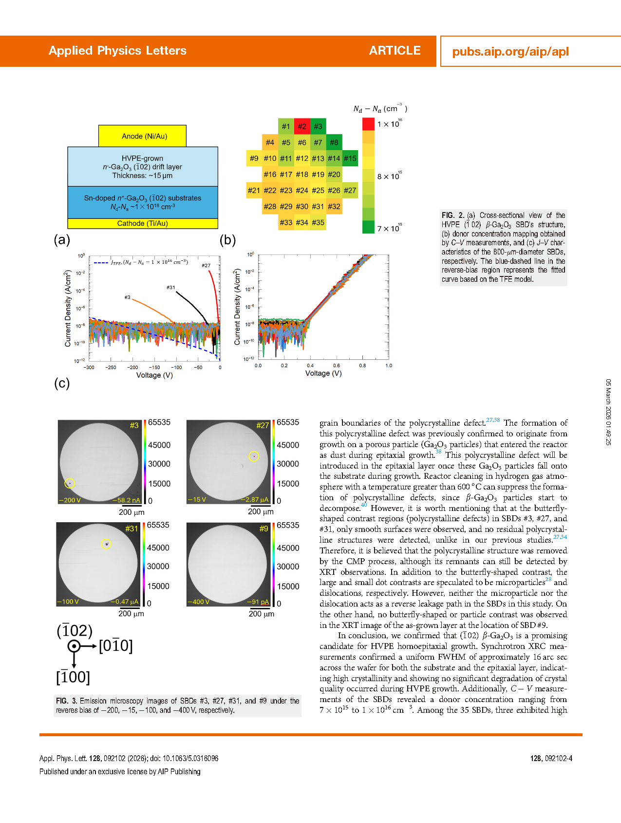
FIG. 4. Synchrotron XRT images of (a) SBDs #3, #27, #31, and #9 after electrical measurements, and (b) their corresponding as-grown epilayers at the electrode positions.
DOI:
doi.org/10.1063/5.0316096