Paper Sharing
【Member Papers】Real-time evolution of performance in β-Ga₂O₃ Schottky barrier diodes under on-state stress
日期:2026-03-11阅读:303
Researchers from the Nanjing University of Posts and Telecommunications have published a dissertation titled "Real-time evolution of performance in β-Ga2O3 Schottky barrier diodes under on-state stress" in Applied Physics Letters.
Project Support
This work was supported in part by the National Natural Science Foundation of China under Grant Nos. 62304113 and 62204126 and in part by the National Key R&D Program of China under Grant No. 2022YFB3605404.
Background
Ultra-wide bandgap semiconductor β-Ga2O3 possesses a bandgap of up to 4.9 eV and a breakdown field of 8 MV/cm. This, coupled with its high Baliga’s figure of merit, positions β-Ga2O3 as a promising candidate for next-generation power electronic devices. The availability of cost-effective, large-scale β-Ga2O3 single crystal substrates further strengthens its candidacy for power applications. However, β-Ga2O3 faces the challenge of intrinsically low thermal conductivity. Low thermal conductivity can exacerbate degradation at the metal–semiconductor interface, which is a critical concern during high-power on-state operation, thereby undermining device reliability.
Abstract
β-Ga2O3 is rapidly emerging as a leading material for next-generation high-power electronic devices due to its exceptional material properties, such as a high breakdown field and a superior Baliga's figure of merit. Vertical β-Ga2O3 Schottky barrier diodes (SBDs) offer advantages, including high on-current density and efficient chip area utilization; however, these benefits also result in elevated power density. Due to the low thermal conductivity of β-Ga2O3, the junction temperature during forward operation is potentially higher than that of SiC and GaN devices, which poses a greater challenge to its long-term reliability. A comprehensive understanding of the on-state reliability for the β-Ga2O3 SBDs is still lacking. Here, we address this gap by employing a measure–stress–measure approach to systematically investigate the real-time degradation and recovery behavior of key performance parameters—turn-on voltage (Von) and on-resistance (Ron)—in the β-Ga2O3 SBDs. We subject these devices to prolonged forward bias stress (5–9 V) and varying temperature conditions (25–125 °C) to assess their degradation characteristics and mechanisms. Notably, at an operating temperature of 125 °C, these β-Ga2O3 SBDs are projected to function reliably for almost a decade at an operating voltage of 1.46 V, assuming a 5% shift in Von as the failure criterion. This exceptional robustness, attributed to both the inherent material properties of β-Ga2O3 and the quality of the β-Ga2O3 Schottky interface, highlights the potential of β-Ga2O3 for long-term, high-performance applications in demanding power electronics.
Conclusion
In conclusion, this study investigates the performance degradation and recovery mechanisms of vertical β-Ga2O3 SBDs under on-state stress, using an MSM technique. The research explores the impact of stress voltage and temperature on key parameters, including Von and Ron. The results show that both stress voltage and temperature strongly influence the degradation, with higher voltages and temperatures accelerating the degradation and increasing the non-recoverable degradation. Analyses of the reverse leakage current, together with the STEM results, indicate that the non-recoverable degradation originates from alterations at the interface. The lifetime prediction using the MSM technique suggests that the devices could operate reliably for nearly a decade at a standard operating voltage and room temperature, demonstrating their potential as a promising material for next-generation power devices.
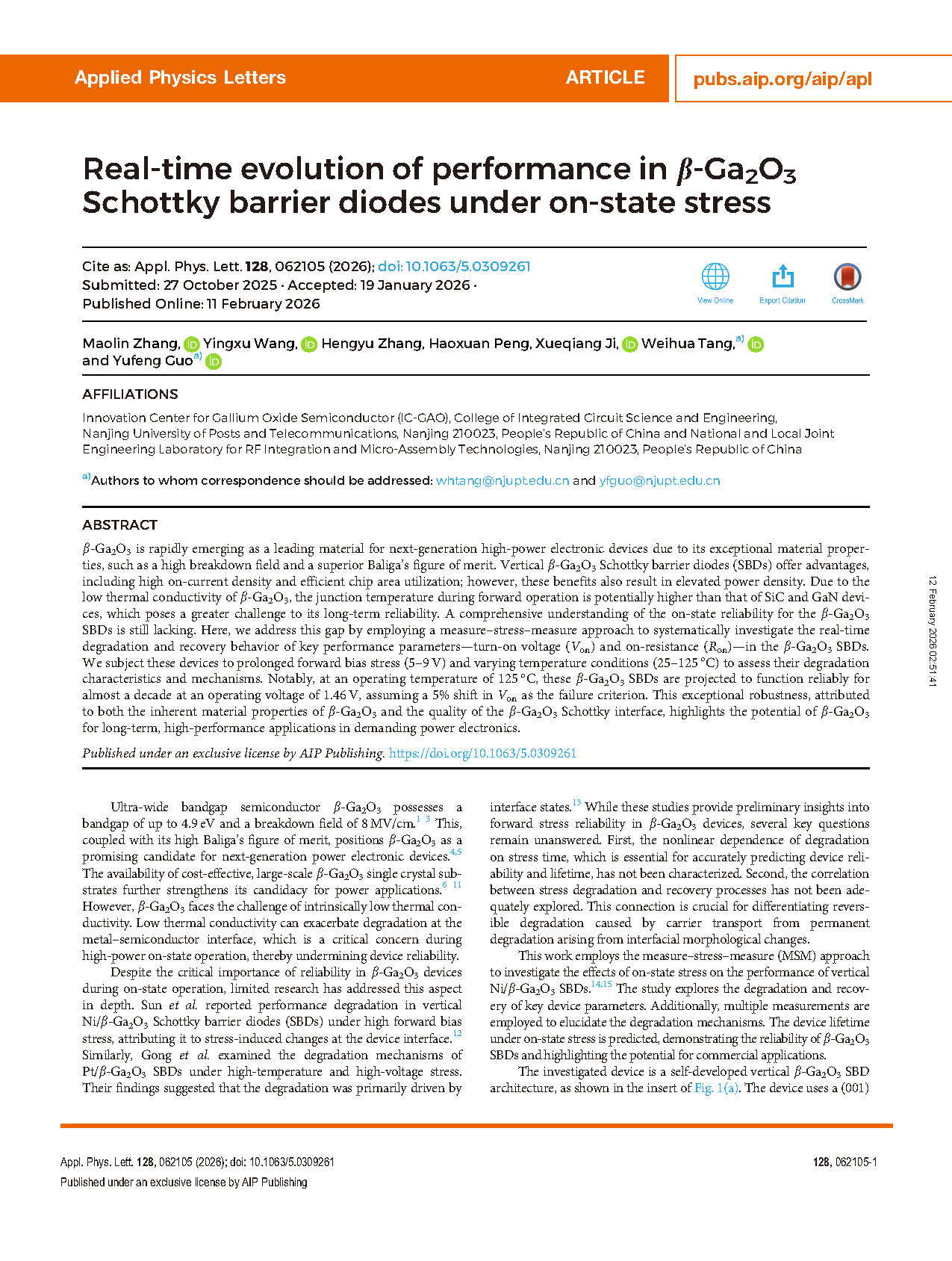
FIG. 1. (a) The structure of the vertical β-Ga2O3 SBDs and the screening results of forward characteristics for the β-Ga2O3 SBDs. (b) Logarithmic scale forward and leakage current (measured by high-resolution source-measure unit) characteristics of the screened devices. (c) Breakdown characteristics (measured by high-voltage source-measure unit) of the screened devices. (d) Schottky barrier height (qΦB) as a function of q/2kT for the screened SBD. The inset shows the modified Richardson plot, where the A* is the Richardson constant and σ0 is the standard deviation. (e) The schematic diagram of the measure–stress–measure testing setups.
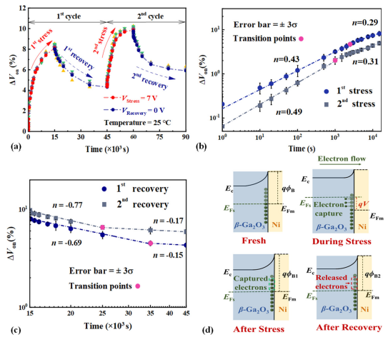
FIG. 2. (a) Real-time Von degradation and recovery in four random SBDs during two on-state stress and recovery cycles. (b) and (c) are the Von degradation and recovery over time on a logarithmic scale. (d) Energy band diagrams of the Ni/Ga2O3 interface under different states.

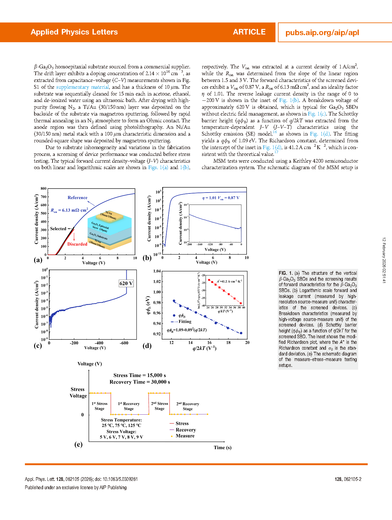
FIG. 3. Temperature-dependent reverse J–V characteristics of (a) the fresh SBD and (b) stressed (7 V) SBD. (c) ln(J/T2) as a function of F1/2 of the fresh SBD. (d) ln(J/F) as a function of F1/2 of the stressed SBD. (e) Sfit/Scal of the fresh and stressed SBDs. (f) Intercept of the ln(J/F)–F1/2 curve as a function of temperature for the stressed SBD. (g) STEM images of the interface morphology and elements mapping for the fresh and stressed SBDs.
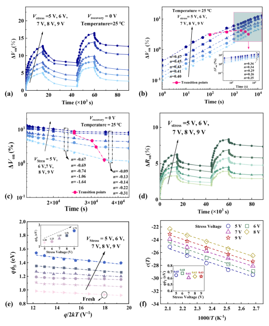
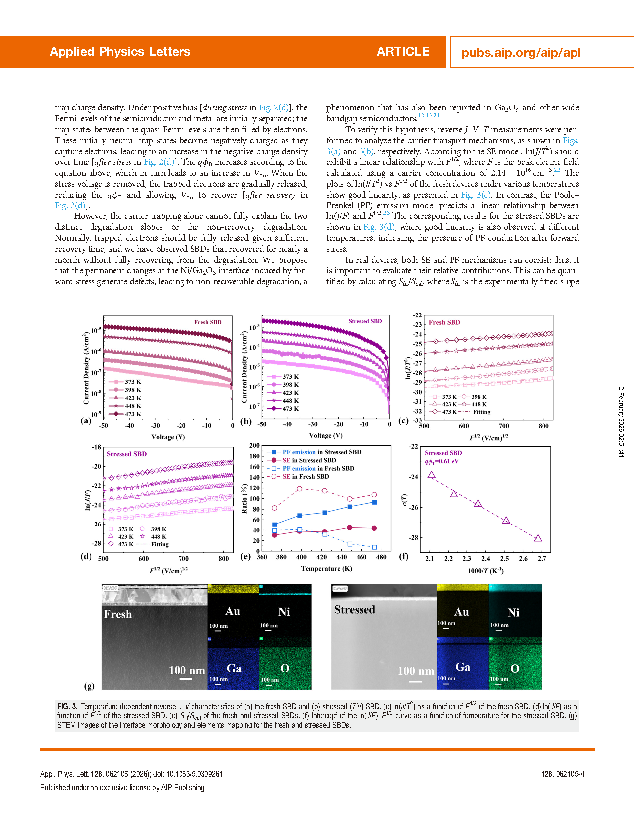
FIG. 4. (a) Real-time Von degradation and recovery under different voltage stresses. (b) and (c) are the Von degradation and recovery upon different voltage stresses presented on a logarithmic scale. (d) Real-time Ron degradation and recovery under different voltage stresses. (e) The fitting qΦB as a function of the stress voltage. (f) Extracted qΦT of the stressed SBD under different stress voltages.
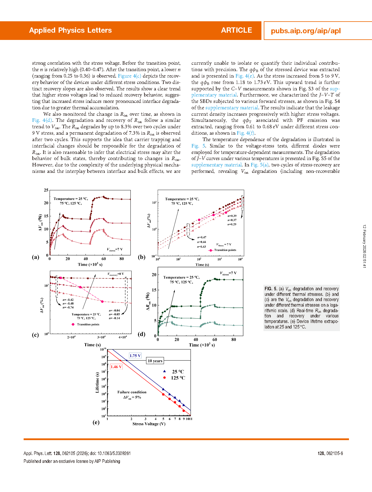
FIG. 5. (a) Von degradation and recovery under different thermal stresses. (b) and (c) are the Von degradation and recovery under different thermal stresses on a logarithmic scale. (d) Real-time Ron degradation and recovery under various temperatures. (e) Device lifetime extrapolation at 25 and 125 °C.
DOI:
doi.org/10.1063/5.0309261