


Paper Sharing
【International Papers】Phonon Thermal Transport and Cooling Limits in Submicron Heteroepitaxial β-Ga₂O₃ Films on SiC
日期:2026-03-12阅读:311
Background
β-Ga₂O₃ possesses an ultra-wide bandgap (4.8 eV) and a high critical electric field (8 MV cm⁻¹), making it highly promising for power and RF devices. However, its extremely low thermal conductivity (11–27 W m⁻¹ K⁻¹) leads to severe self-heating at high power levels, with channel temperatures potentially exceeding 1500 °C. This issue has become a major bottleneck for its commercialization. Integrating β-Ga₂O₃ heterogeneously on high-thermal-conductivity SiC substrates is considered a mainstream approach to improve thermal management. Compared with wafer bonding, direct epitaxial growth can avoid problems such as high interfacial thermal resistance and difficulty in thickness control, while also benefiting from the relatively small lattice mismatch between β-Ga₂O₃ and SiC. However, current understanding of phonon transport, interfacial thermal conductance, and cooling limits in submicron β-Ga₂O₃ films remains limited, which constrains further optimization of thermal design. Therefore, there is an urgent need to develop precise thermal characterization methods to reveal the mechanisms of heat transport and determine the cooling limits of devices, thereby promoting practical applications.
Abstract
Heterogeneous integration of β-phase gallium oxide (β-Ga2O3) with high-thermal-conductivity substrates such as SiC offers a promising route toward improved thermal management in ultrawide bandgap β-Ga2O3 power devices. Here, we systematically investigate phonon thermal transport and cooling limits in submicron β-Ga2O3 thin films on SiC. Frequency-domain thermoreflectance measures the thermal conductivities and thermal boundary conductances (TBCs) of 0.1–1 μm β-Ga2O3 thin films grown by metal-organic chemical vapor deposition on 4H-SiC and c-plane sapphire substrates. The thermal conductivities are found to depend on both film thickness and crystallinity, with the 0.1 μm films exhibiting among the highest values reported to date for β-Ga2O3 films of comparable thickness. The β-Ga2O3/SiC interface exhibits a relatively high TBC of ∼90 MW m–2 K–1, compared to values previously reported for bonded β-Ga2O3/SiC and β-Ga2O3/diamond interfaces. Scanning transmission electron microscopy and elemental mapping analyses confirm that this heterointerface is structurally and compositionally distinct. Semiclassical phonon transport theory predicts potential improvements in the phonon thermal properties. Based on these predictions, device thermal modeling reveals that heterointegration with SiC can fundamentally boost phononic cooling in lateral β-Ga2O3 transistors—particularly at a reduced Ga2O3 thickness of ∼0.1 μm—achieving thermal performance comparable to, or even surpassing, that of current state-of-the-art wide bandgap GaN devices.
Research Results
Recently, a research team led by Professor Jungwan Cho from Sungkyunkwan University and Professor Dae-Woo Jeon from the Korea Institute of Ceramic Engineering and Technology achieved a significant breakthrough in thermal transport studies of wide-bandgap semiconductor heterostructures. Their work systematically investigated phonon thermal transport characteristics and device cooling limits in submicron heteroepitaxial β-Ga₂O₃ films grown on SiC substrates. The study revealed the dependence of thermal conductivity on film thickness and crystallinity, as well as the efficient heat-transport mechanism across the β-Ga₂O₃/SiC interface, providing new theoretical and experimental insights for optimizing thermal management in β-Ga₂O₃ devices.
The research team employed metal-organic chemical vapor deposition (MOCVD) to grow β-Ga₂O₃ epitaxial films with thicknesses ranging from 0.1 to 1 μm on 4H-SiC and c-plane sapphire substrates. Frequency-domain thermoreflectance (FDTR) was used to accurately measure the cross-plane thermal conductivity of the films and the interfacial thermal conductance. Combined with scanning transmission electron microscopy (STEM), energy-dispersive spectroscopy (EDS), and X-ray diffraction (XRD), the team analyzed the interfacial structure and film crystallinity. Furthermore, by integrating semiclassical phonon transport theory with finite-element thermal modeling of devices, the phononic cooling limit of β-Ga₂O₃/SiC heterogeneously integrated devices was clarified.
The results show that the thermal conductivity of β-Ga₂O₃ films strongly depends on thickness and crystallinity. A 0.1 μm-thick film exhibits the highest thermal conductivity reported so far for films of similar thickness. The β-Ga₂O₃/SiC interface demonstrates a high interfacial thermal conductance of approximately 90 MW m⁻² K⁻¹, significantly outperforming interfaces produced by conventional bonding methods such as β-Ga₂O₃/SiC and β-Ga₂O₃/diamond. STEM and EDS analyses confirm that the heterointerface is structurally and compositionally abrupt, with no evident elemental interdiffusion or amorphous layers.
Semiclassical phonon transport theory successfully explains how boundary scattering and defect scattering regulate the thermal conductivity of the films. Device thermal modeling based on the experimental data indicates that when the β-Ga₂O₃ film thickness is reduced to around 0.1 μm, the thermal performance of laterally integrated β-Ga₂O₃ transistors on SiC can match or even surpass that of the most advanced GaN devices. In this case, the power density can reach 10.8 W mm⁻¹ with a thermal resistance as low as 16.5 mm K W⁻¹.
This study provides a rational optimization strategy for thermal management in ultra-wide-bandgap β-Ga₂O₃ power devices and establishes a critical foundation for their application in high-power electronics. The related research was published in the leading materials science journal Acta Materialia under the title “Phonon Thermal Transport and Cooling Limits in Submicron Heteroepitaxial β-Ga₂O₃ Films on SiC.”
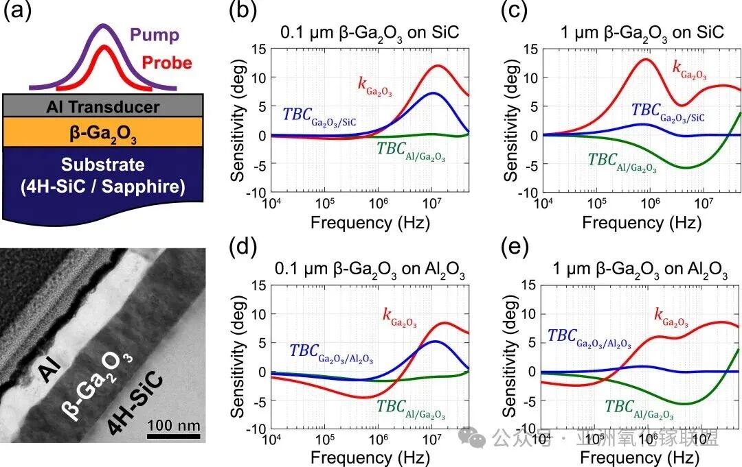
Figure 1.(a) Cross-sectional schematic of MOCVD-grown β-Ga₂O₃ films on 4H-SiC and c-plane sapphire substrates, together with a representative cross-sectional TEM image of the 0.1 μm β-Ga₂O₃/SiC structure.(b–e) Sensitivity curves of FDTR measurements for the thermal conductivity of β-Ga₂O₃ films (kGa₂O₃) and the thermal boundary conductance at the upper and lower interfaces (TBC_Al/Ga₂O₃ and TBC_Ga₂O₃/Substrate). Panels (b) and (c) correspond to 0.1 μm and 1 μm β-Ga₂O₃/SiC, while (d) and (e) correspond to 0.1 μm and 1 μm β-Ga₂O₃/sapphire, respectively.
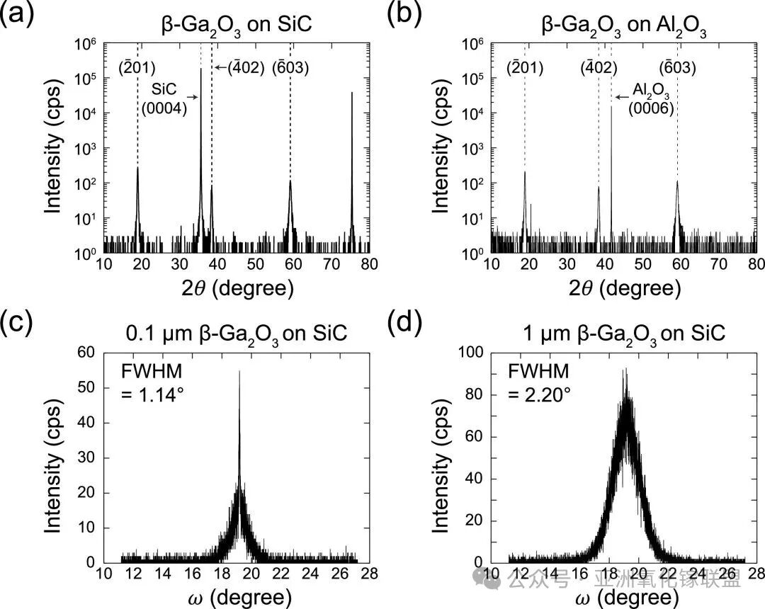
Figure 2. XRD characterization of β-Ga₂O₃ thin films.(a, b) XRD 2θ scan patterns of β-Ga₂O₃ films grown on 4H-SiC and c-plane sapphire substrates, respectively. The characteristic β-Ga₂O₃ peaks (2̅01), (4̅02), and (6̅03), together with the substrate peaks, are clearly identified, confirming that the films exhibit a single (2̅01) orientation.(c, d) XRD rocking curves of the (4̅02) peak for 0.1 μm and 1 μm β-Ga₂O₃/SiC films, respectively. The full width at half maximum (FWHM) values are 1.14° and 2.20°, indicating that the crystallinity decreases with increasing film thickness.
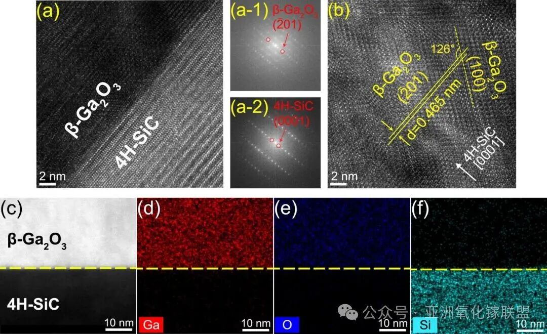
Figure 3. High-resolution structural and compositional characterization of the β-Ga₂O₃/SiC heterointerface. (a) High-resolution TEM (HR-TEM) image of the β-Ga₂O₃/SiC interface, showing an abrupt interface without three-dimensional island growth. The inset presents fast Fourier transform (FFT) patterns of β-Ga₂O₃ and 4H-SiC, confirming the epitaxial relationship between the β-Ga₂O₃ (2̅01) film and the SiC (0001) substrate. (b) HR-TEM image of the β-Ga₂O₃ film, where clear (2̅01) lattice fringes with an interplanar spacing of 0.465 nm are observed, forming an angle of 126° with the (100) plane, consistent with the monoclinic crystal structure. (c) High-angle annular dark-field (HAADF) STEM image of the β-Ga₂O₃/SiC interface, revealing a sharp contrast change at the interface. (d–f) EDS elemental mapping of Ga, O, and Si, confirming that the elements are strictly confined within their respective layers with no evident interdiffusion across the interface.
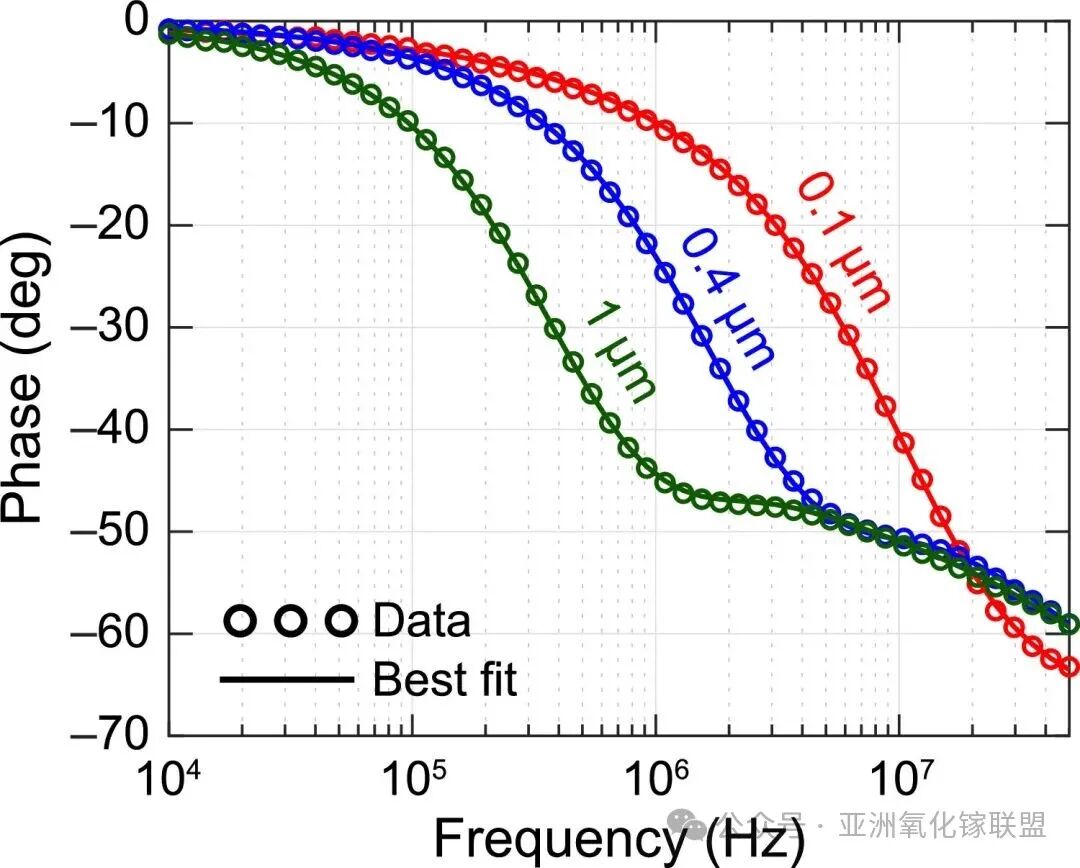
Figure 4. FDTR phase experimental data and thermal model fitting curves for β-Ga₂O₃ films with different thicknesses on 4H-SiC substrates. The fitted curves for the 0.1 μm, 0.4 μm, and 1 μm films agree well with the experimental data, confirming the reliability of the thermal model and the accuracy of the measurements.
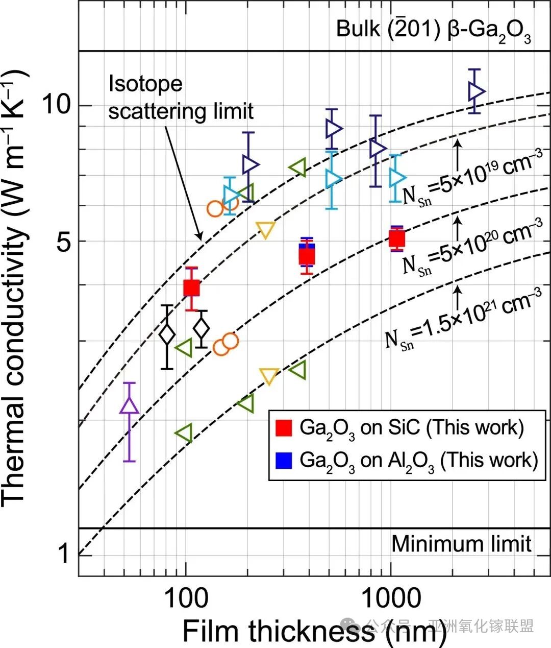
Figure 5. Thickness dependence of the cross-plane thermal conductivity of (2̅01)-oriented β-Ga₂O₃ films at room temperature. The β-Ga₂O₃ films grown on SiC and sapphire substrates in this work (solid squares) are compared with data reported in the literature (open symbols). The figure also includes the bulk thermal conductivity of β-Ga₂O₃, the minimum thermal conductivity of amorphous Ga₂O₃, and the predicted phonon thermal transport curves for different Sn doping concentrations (black dashed lines). The results show that the thermal conductivity increases with film thickness and is strongly regulated by defect scattering. The 0.1 μm film exhibits the highest thermal conductivity reported for films of the same thickness.
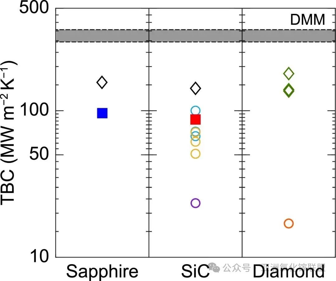
Figure 6. Comparison of the interfacial thermal conductance between β-Ga₂O₃ and three substrates—sapphire, SiC, and diamond—at room temperature. The measurements from this work (solid squares) are compared with literature data (open symbols). The theoretical upper limit predicted by the diffuse mismatch model (DMM) is also shown (red dashed line). The results demonstrate that epitaxially grown β-Ga₂O₃/substrate interfaces exhibit significantly higher thermal conductance than those fabricated by bonding methods. In particular, the β-Ga₂O₃/SiC interface shows a thermal conductance of approximately 90 MW m⁻² K⁻¹, close to that of epitaxially grown β-Ga₂O₃/sapphire interfaces.
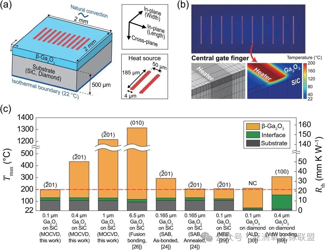
Figure 7. Finite-element thermal modeling and performance analysis of lateral multi-finger β-Ga₂O₃ transistors. (a) Schematic structure of the simulated device, consisting of 10 gate fingers with a variable Ga₂O₃ layer thickness. The heat generation region is modeled as a rectangular surface heater. The bottom of the substrate is defined as an isothermal boundary, while the other surfaces are subject to natural convection. (b) Representative finite-element mesh and steady-state temperature distribution for a 1 μm β-Ga₂O₃/SiC device. (c) Comparison of the maximum temperature (left axis) and thermal resistance (right axis) of devices based on different β-Ga₂O₃ heterostructures. The 0.1 μm β-Ga₂O₃/SiC device in this work exhibits the lowest thermal resistance, outperforming previously reported β-Ga₂O₃/SiC and β-Ga₂O₃/diamond heterostructures.
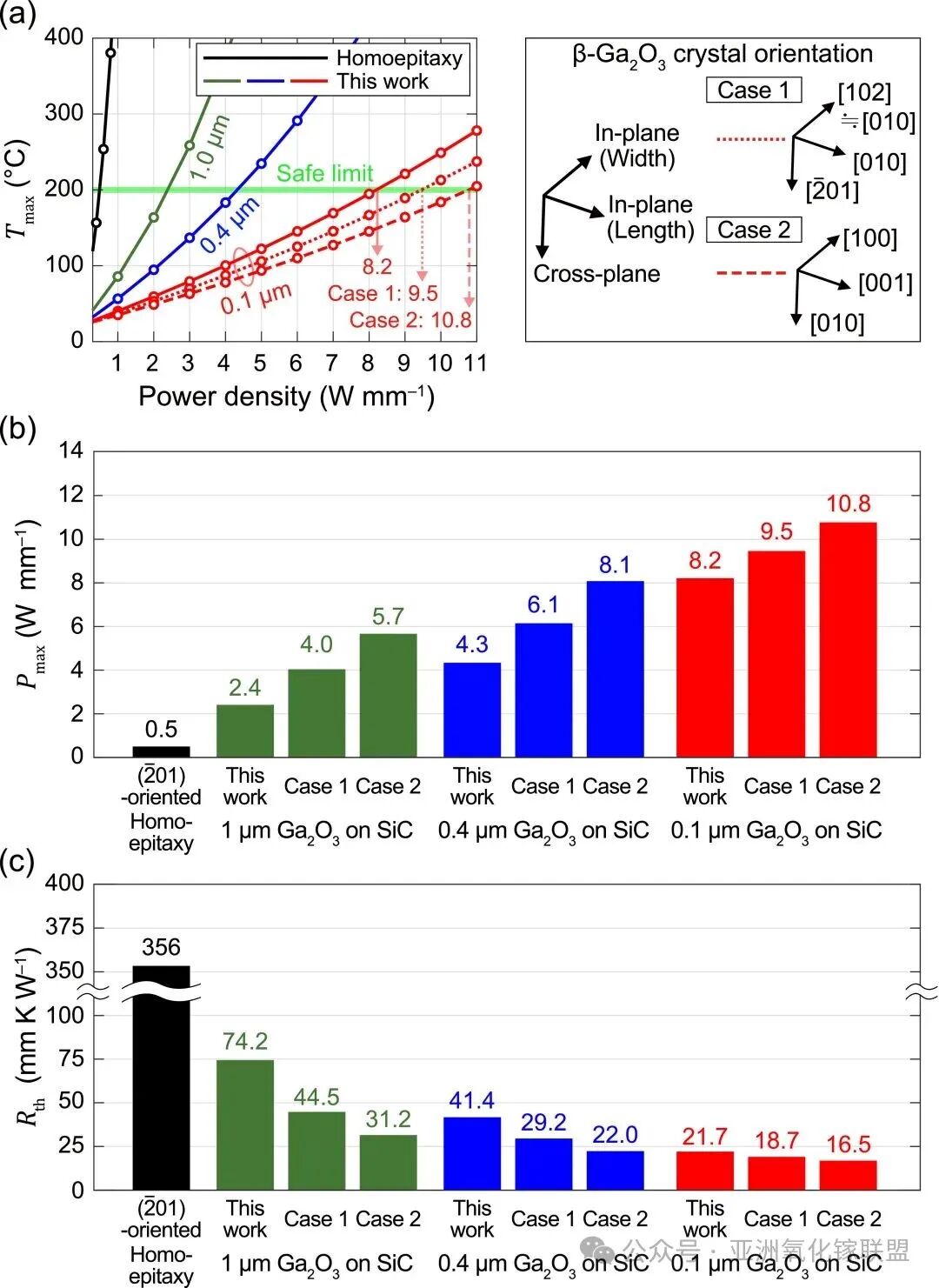
Figure 8. Comparison of the thermal performance between β-Ga₂O₃/SiC devices and homoepitaxial β-Ga₂O₃ devices. (a) Variation of the maximum device temperature with dissipated power density for β-Ga₂O₃/SiC devices with different film thicknesses. The predicted curve for an ideally oriented 0.1 μm β-Ga₂O₃/SiC device is also shown, with a safe junction temperature of 200°C taken as the performance limit. (b) Comparison of the maximum tolerable power density (Pmax) for different devices. The 0.1 μm β-Ga₂O₃/SiC device reaches a Pmax of 8.2 W mm⁻¹, which can increase to 10.8 W mm⁻¹ for an ideal crystal orientation—about 16 times higher than that of homoepitaxial devices. (c) Comparison of thermal resistance (Rth) for different devices. The 0.1 μm β-Ga₂O₃/SiC device exhibits an Rth of 21.7 mm K W⁻¹, which can be reduced to 16.5 mm K W⁻¹ under ideal orientation conditions, comparable to or even surpassing GaN-on-SiC and GaN-on-diamond devices.
DOI:
doi.org/10.1016/j.actamat.2026.122020
