Paper Sharing
【Member Papers】Impact of Proton Irradiation and Oxygen Annealing on the Photoluminescence and Bandgap of β-Ga₂O₃ Epitaxial Wafer
日期:2026-03-12阅读:323
Researchers from the Sichuan University have published a dissertation titled "Impact of Proton Irradiation and Oxygen Annealing on the Photoluminescence and Bandgap of β-Ga2O3 Epitaxial Wafer" in Journal of Alloys and Compounds.
Project Support
This work was supported by the National Natural Science Foundation of China under Grant No. 61974096. We would like to thank the Analytical & Testing Center of Sichuan University for XPS work and we would be grateful to Shuguang Yan for his help of XPS analysis. We would like to thank Dr Wu, Peng & Dr. Yanying, Wang of Analytical & Testing Center Sichuan University for their assistance on steady/transient fluorescence. We sincerely thank Prof. Li Wu at Analytical & Testing center of Sichuan University for the measurement of Raman.
Abstract
Defect control is crucial for the advancement of β-Ga2O3 based optoelectronics. This study systematically investigates the effect of defects and optoelectronic properties in β-Ga2O3 epitaxial wafers through 5 MeV proton irradiation and subsequent high-temperature oxygen annealing. Proton irradiation induces the disruption of Ga-O bonds, generating complex defects, including oxygen vacancy (VO), gallium vacancy (VGa), gallium and oxygen divacancy (VGa-VO), and oxygen interstitial (Oi), leading to significant photoluminescence quenching and bandgap narrowing. Notably, at an ultra-fluence of 1 × 10¹⁶ p/cm2, a partial in-situ recovery of the structure and defect states occurs due to irradiation-induced thermal annealing effects, post-irradiation oxygen annealing effectively repairs the lattice damage, especially restoring optical and structural properties to their pre-irradiation state, achieved after annealing at 900 ℃. This work elucidates the damage and recovery dynamics of β-Ga2O3 under proton irradiation and thermal processing, providing vital insights for defect engineering to tailor its properties for advanced photodetectors and neuromorphic optoelectronic devices.
Highlights
● Proton irradiation induces the significant decline in β-Ga2O3 PL intensity.
● The oxygen vacancies induced proton irradiation by narrow the β-Ga2O3 bandgap.
● High-temperature oxygen annealing effectively restores the damage caused by proton irradiation.
● In-situ annealing resulted from high fluence proton irradiation partially recovers the damage in β-Ga2O3 epitaxial layer.
Conclusion
In summary, this study systematically investigates the influences of 5 MeV proton irradiation and subsequent high-temperature oxygen post-annealing on the crystalline structure, defect states, and optical absorption properties of the β-Ga2O3 epitaxial wafers. The results reveal that proton irradiation causes minimal disruption on the overall crystalline structure and quality, with primary damage occurring at the GaⅠO4 units. However, proton irradiation significantly increases the formation of nonradiative defects, resulting in a marked decrease in PL intensity. Furthermore, proton irradiation promotes the generation of radiative defects, such as VO, VGaI-VOⅢ0 or VGaI-VOI1-, VGaI2-, and Oi0. Most of induced VO defects are associated with the oxygen located at the OⅠ site, consequently leading to Eg narrowing. Meanwhile, the epitaxial layer in S16 exhibits partially restored crystallinity due to the annealing effects during irradiation. High-temperature oxygen post-annealing is effective in repairing irradiation-induced defects and recovering crystal quality. Overall, these findings offer valuable insights for defect engineering in β-Ga2O3 PDs and photoelectronic bionic synapses.
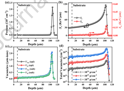
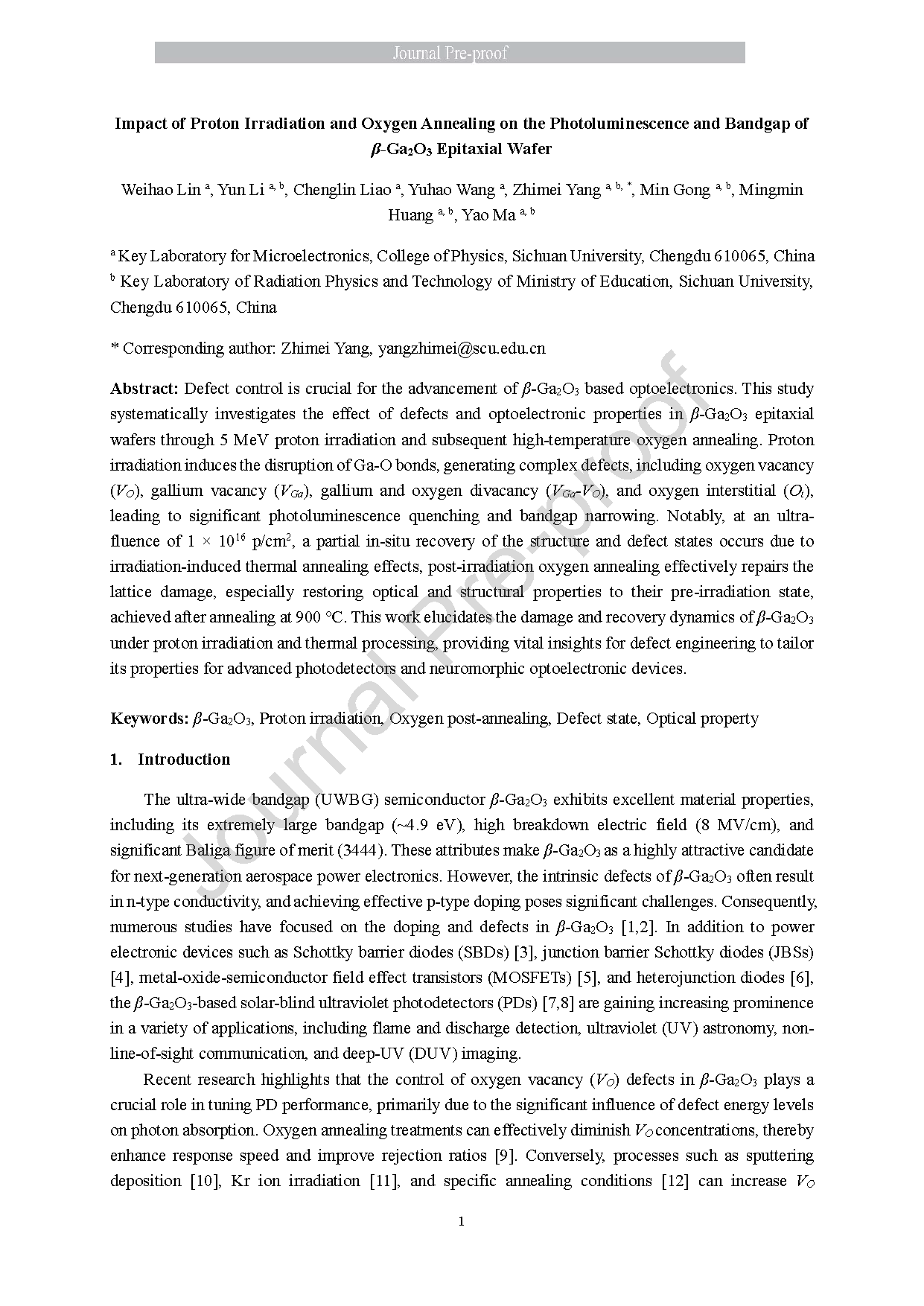
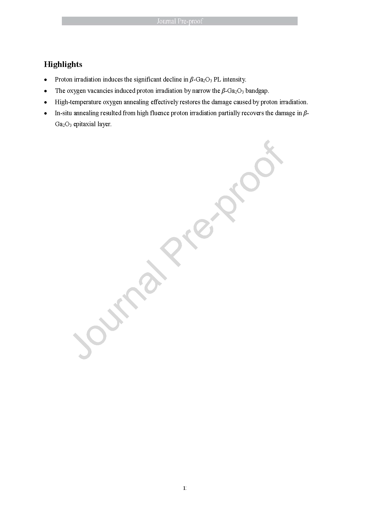
Fig. 1. The SRIM simulation results of (a) the distribution of protons; (b) the depth profiles of Se and Sn; (c) the distribution of VO and VGa at each layer and (d) VO+VGa under different fluences.
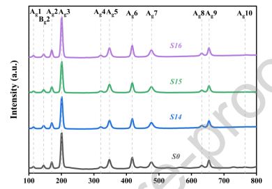
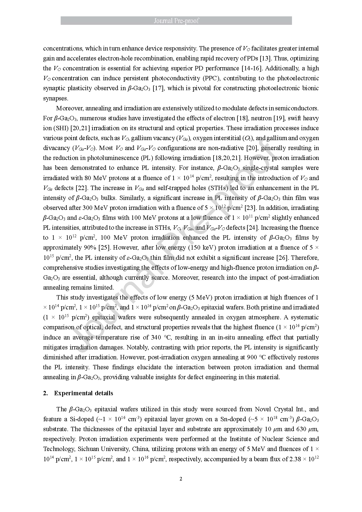
Fig. 2. The Raman spectra of S0, S14, S15, and S16 under room temperature.
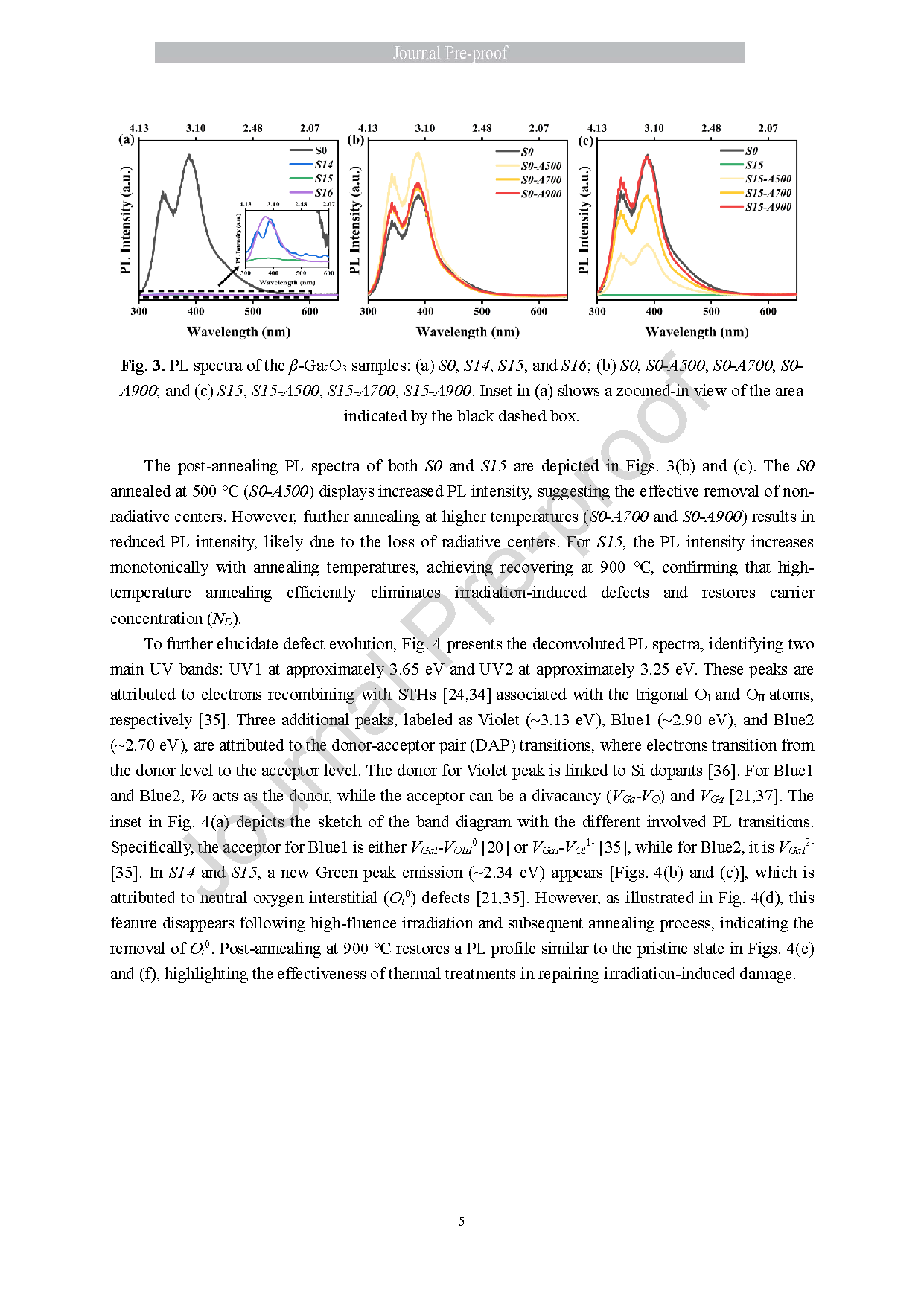
Fig. 3. PL spectra of the β-Ga2O3 samples: (a) S0, S14, S15, and S16; (b) S0, S0-A500, S0-A700, S0- A900; and (c) S15, S15-A500, S15-A700, S15-A900. Inset in (a) shows a zoomed-in view of the area indicated by the black dashed box.
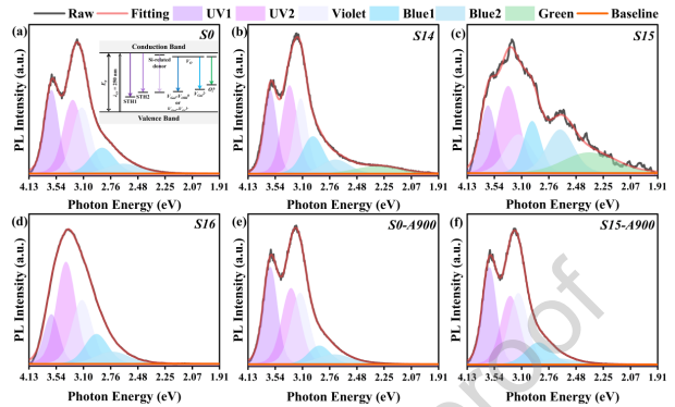
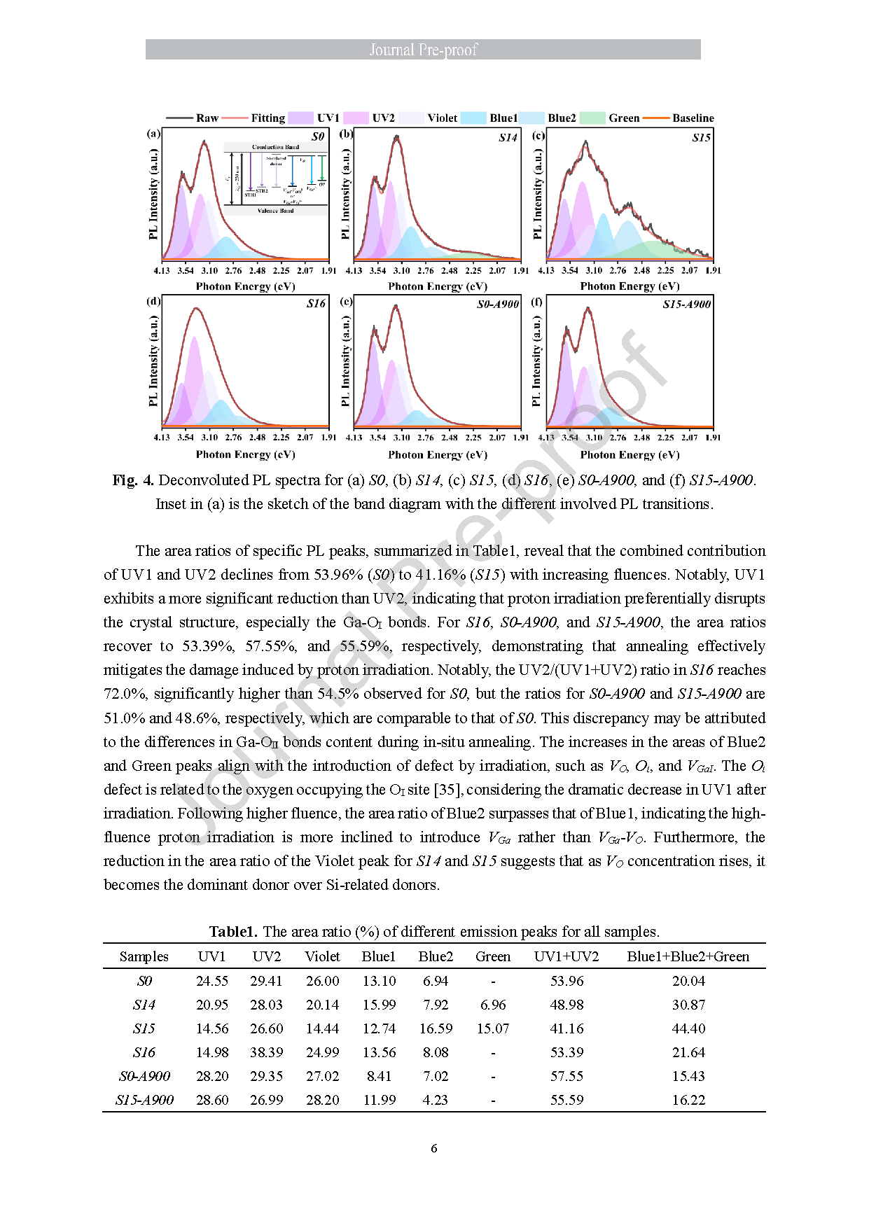
Fig. 4. Deconvoluted PL spectra for (a) S0, (b) S14, (c) S15, (d) S16, (e) S0-A900, and (f) S15-A900. Inset in (a) is the sketch of the band diagram with the different involved PL transitions.

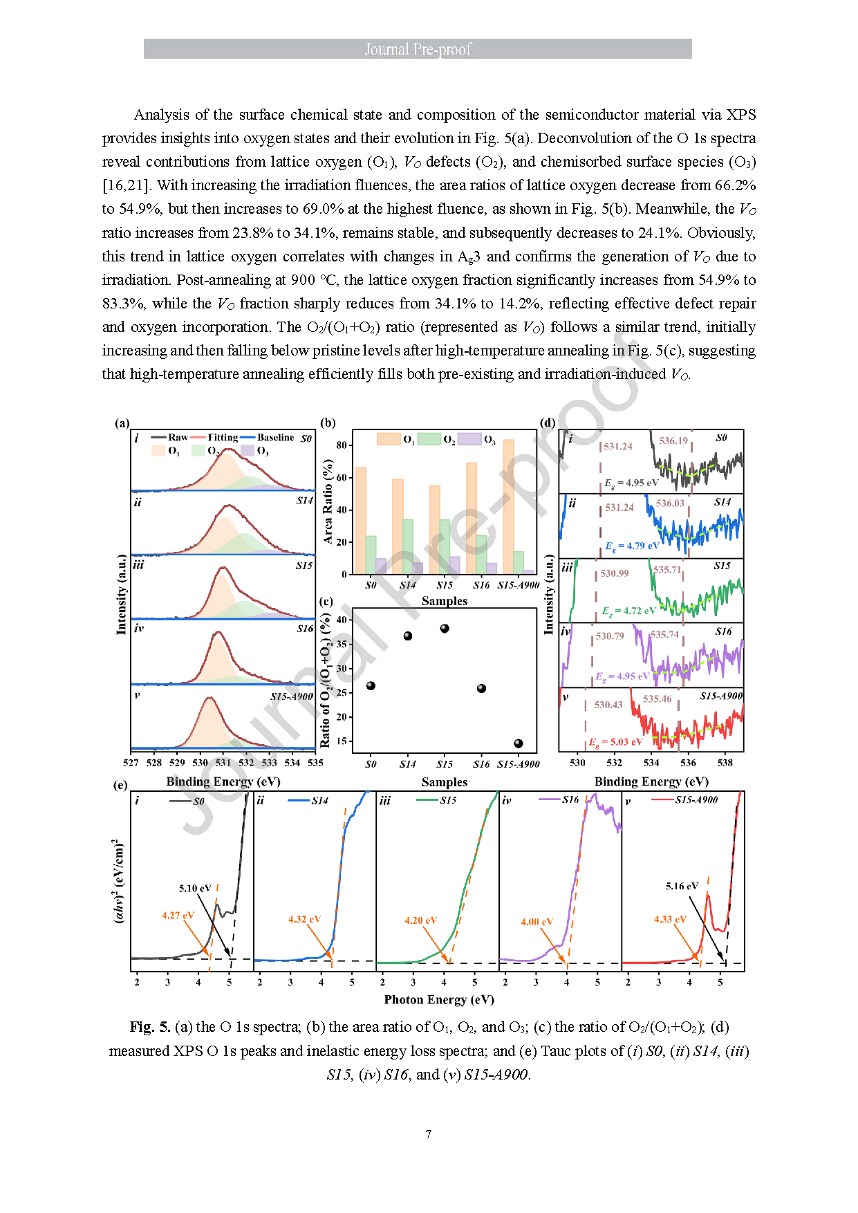
Fig. 5. (a) the O 1s spectra; (b) the area ratio of O1, O2, and O3; (c) the ratio of O2/(O1+O2); (d) measured XPS O 1s peaks and inelastic energy loss spectra; and (e) Tauc plots of (i) S0, (ii) S14, (iii) S15, (iv) S16, and (v) S15-A900.
DOI:
doi.org/10.1016/j.jallcom.2026.187124