Paper Sharing
【Domestic Papers】Effects of fluorine on the optoelectronic properties and crystal field symmetry of silicon-based erbium doped gallium oxide films and devices
日期:2026-03-12阅读:291
Researchers from the Zhejiang University have published a dissertation titled "Effects of fluorine on the optoelectronic properties and crystal field symmetry of silicon-based erbium doped gallium oxide films and devices" in Applied Physics A.
Project Support
This work was supported by the Key Research Project of Zhejiang Province (Grant No. 2024C01054).
Background
With the shrinking feature size of integrated circuits (ICs), problems of signal crosstalk and power consumption in conventional IC systems based on electrical interconnection has become more and more serious. To address these issues, silicon-based optoelectronics has emerged, which combines the mature technology of silicon-based microelectronics and advantages of photons as the information carrier. However, to accomplish silicon-based optoelectronics, effective silicon-based light sources should be obtained. Among all the candidates, silicon-based erbium (Er) doped light-emitting devices (LEDs) has aroused extensive attention because the intra-4f transition of the Er3+ ion located in the minimum loss window of quartz fiber (~ 1540 nm), as well as the constant emission wavelength. Nevertheless, both the lack of proper doping hosts and the weak emission performances limit the further development of silicon-based Er doped LEDs.
Abstract
The fluorine co-doped silicon-based erbium doped gallium oxide luminescent device have been fabricated. We have investigated effects of fluorine on the optoelectrical performances of devices and the crystal field symmetry of the environment where erbium ions are located. It is found that with the co-doping of fluorine, the maximum input electrical power of the device can be increased due to the improved conductivity and breakdown field, contributing to the enhanced output intensity of 5.6 µW/cm2. Based on the density functional theory calculation, the crystal field symmetry has been compared. From the symmetry evaluation standard, we have confirmed the preferred occupation site of fluorine doping. Additionally, it is proved that the C4v symmetry of the environment where erbium ions are situated will be degraded with the introduction of fluorine, leading to the remarkedly enhanced optical activity of erbium ions.
Conclusion
In conclusion, effects of F− co-doping on the silicon-based Ga2O3:Er films and devices are investigated based on the experimental results and DFT calculation. We have demonstrated that with the introduction of F−, the grain size of Ga2O3 matrix will become larger due to the release of stress related to the Er3+ doping. For electrical properties, it is found that the introduced donor level will bring about large quantities of free electrons, leading to the pronounced enhancement of carrier concentration from ~1016 cm−3 to ~1020 cm−3. Additionally, the coarse grains will contribute to the higher breakdown field of devices, resulting in the much higher maximum input electric power of 643.0 mW. With regard to emission performances, after the co-doping of F−, the direct PL intensity has been remarkedly increased as a result of the enhanced Er3+ optical activity due to the modified crystal field. For the indirect luminescence, because of the descending concentration of sensitizer VO, the emission intensity of Ga2O3:(Er, F) films and devices have been limited. Nevertheless, thanks to the improved conductivity and breakdown field, the maximum output optical power density of the Ga2O3:(Er, F) device can be increased to 5.6 µW/cm2, 2.7 times higher than the pure Ga2O3:Er device. Besides, we have also established a standard to evaluate the symmetry of the crystal field where Er3+ ions are located based on the standard deviation of Er-O(F) bond length, together with the average difference between O-Er-O(F) bond angles and 90° or 180°. Applying such standard to the constructed Ga63ErO96 and Ga63ErO95F supercells by DFT calculation, we have found that when the OⅠ and OⅢ atoms are substituted, the crystal field symmetry will be broken, while when the OⅡ atom is replaced, a more ordered crystal field will be created. Among such three occasions, the supercell with the OⅠ atom occupied possesses the lowest energy, manifesting that the F atom will mainly substitute the OⅠ atom. Consequently, the symmetry of the crystal field environment where Er3+ ions are situated will be degraded, contributing to the enhanced optical activity.
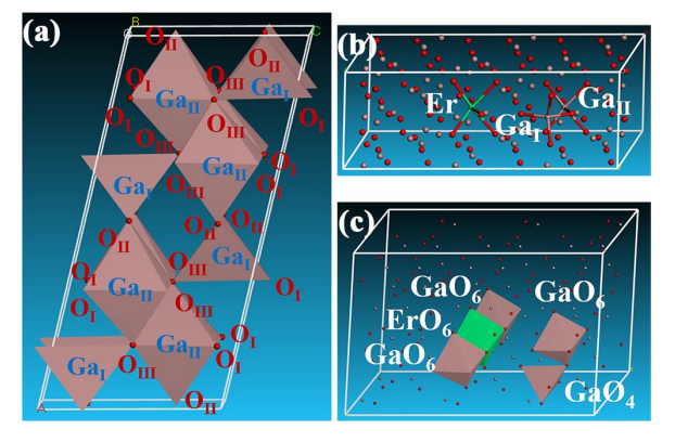
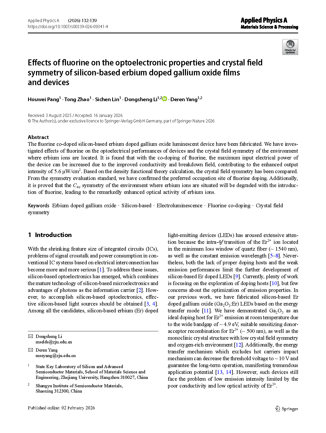
Fig. 1 Schematic diagrams for the structure of (a) Ga2O3 and (b)~(c) Ga63ErO96 supercells by the DFT calculation.
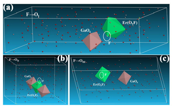
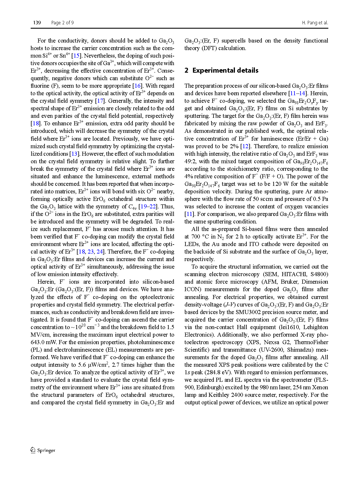
Fig. 2 Structure diagrams of Ga63ErO95F supercells when the F atom substitutes (a) OⅠ, (b) OⅡ and (c) OⅢ atoms by the DFT calculation.
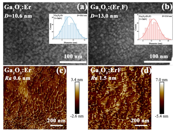
Fig. 3 The surface SEM images and grain size distribution curves of (a) Ga2O3:Er and (b) Ga2O3:(Er, F) films; the surface AFM images of (c) Ga2O3:Er and (d) Ga2O3:(Er, F) films.
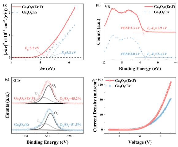
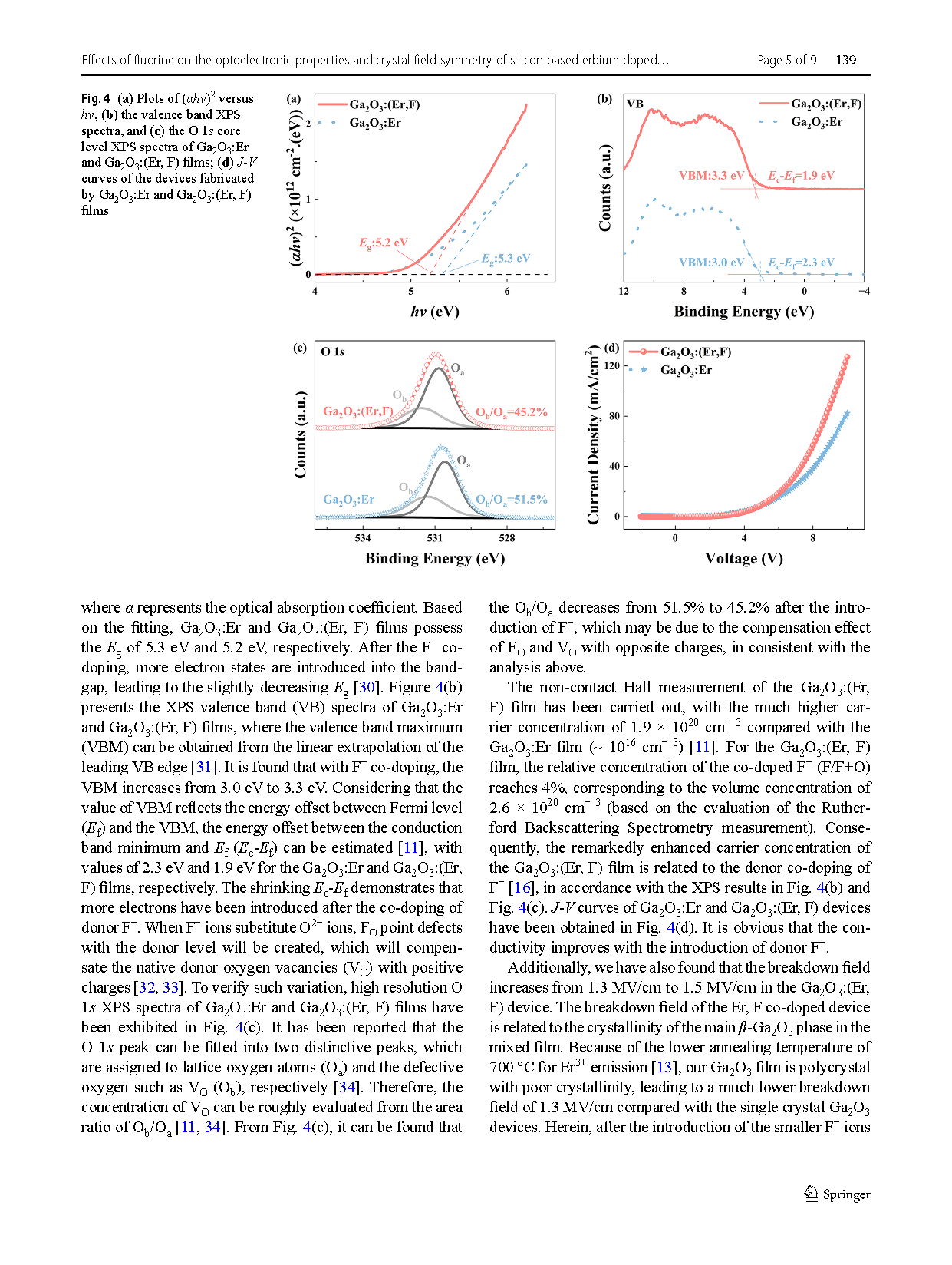
Fig. 4 (a) Plots of (αhv)2 versus hv, (b) the valence band XPS spectra, and (c) the O 1s core level XPS spectra of Ga2O3:Er and Ga2O3:(Er, F) films; (d) J-V curves of the devices fabricated by Ga2O3:Er and Ga2O3:(Er, F) films.
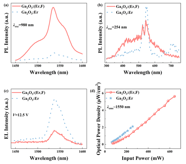
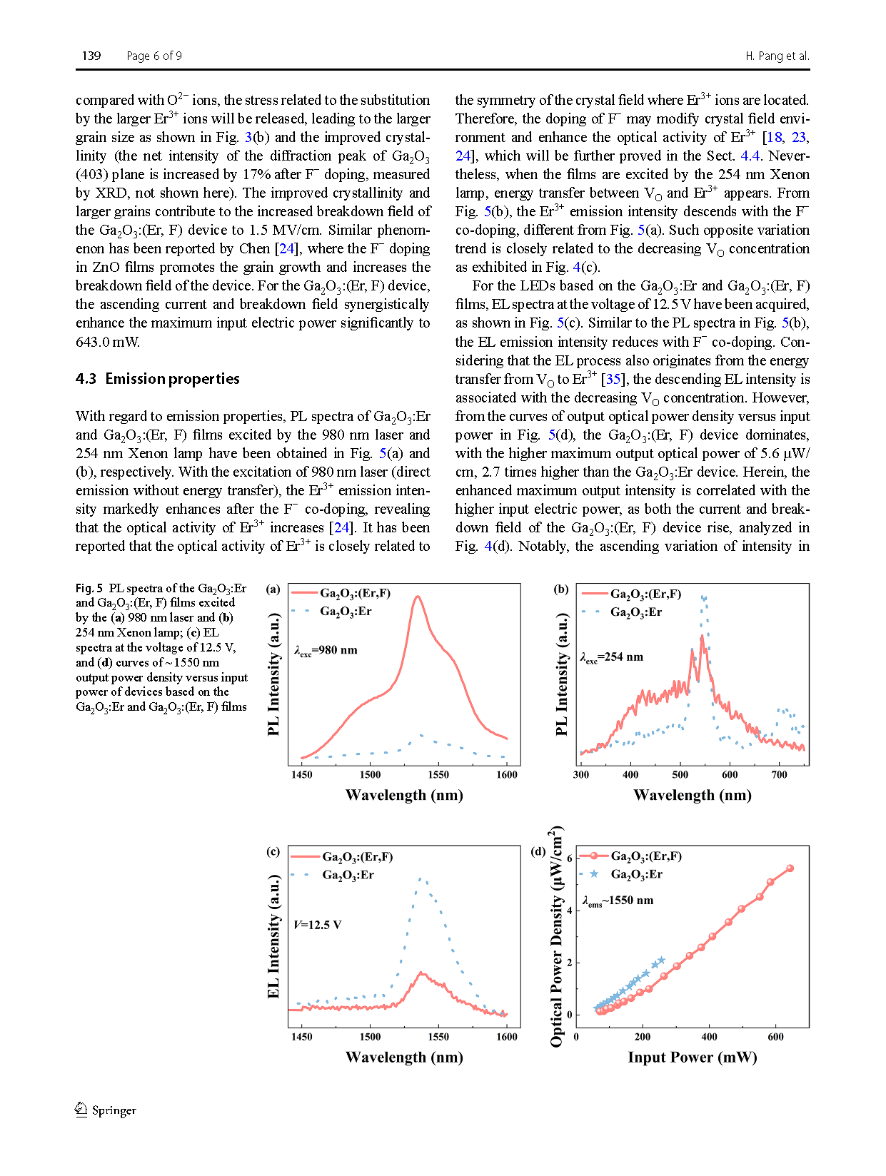
Fig. 5 PL spectra of the Ga2O3:Er and Ga2O3:(Er, F) films excited by the (a) 980 nm laser and (b) 254 nm Xenon lamp; (c) EL spectra at the voltage of 12.5 V, and (d) curves of ~1550 nm output power density versus input power of devices based on the Ga2O3:Er and Ga2O3:(Er, F) films.
DOI:
doi.org/10.1007/s00339-026-09341-4