


Member Intro
【Member Intro】Introduction to Gallium Oxide Epitaxy Technology and Achievements of the Ultra-Wide Bandgap Semiconductor Nanofabrication Platform at the Suzhou Institute of Nano-Tech and Nano-Bionics
日期:2026-03-12阅读:1002
Background
With the continuous development of electronic information technology, wide-bandgap semiconductors such as Silicon Carbide (SiC) and Gallium Nitride (GaN) have achieved large-scale applications in key fields including new-energy vehicles, consumer electronics, AI data centers, and RF communications, owing to their excellent performance under high-voltage, high-frequency, and high-temperature conditions.
As new application scenarios such as 6G communications, ultra-high-voltage power transmission, and large-scale energy storage continue to emerge, ultra-wide-bandgap semiconductor materials—represented by Gallium Oxide (Ga₂O₃), Aluminum Nitride (AlN), hexagonal boron nitride (h-BN), and diamond—are attracting increasing attention from both the global research community and industry. These materials possess higher critical breakdown electric fields as well as superior high-temperature and radiation resistance. As a result, they demonstrate significant potential and value in strategic areas such as high-voltage power devices, deep-ultraviolet optoelectronic devices, electronics for extreme environments, and quantum technologies.
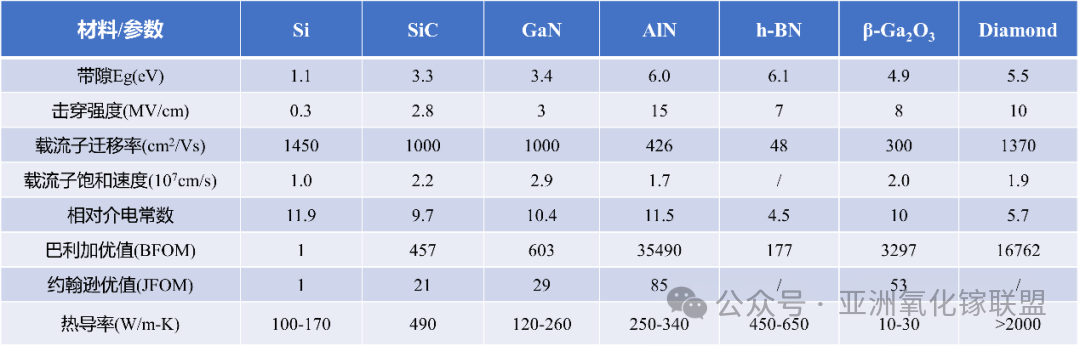
Table 1. Comparison of the Physical Properties of Typical Semiconductor Materials
Epitaxy refers to a semiconductor fabrication technique in which functional material layers with specific structures are grown on single-crystal supporting substrates (such as silicon carbide, sapphire, and silicon) through precise control of growth conditions. This process is typically realized using methods such as metal-organic chemical vapor deposition (MOCVD) and molecular beam epitaxy (MBE). The epitaxial layer and the substrate may be composed of either the same material (homoepitaxy) or different materials (heteroepitaxy). The thickness of epitaxial layers generally ranges from the nanometer scale to the micrometer scale, and in some cases can be even thicker. For semiconductor materials, the fundamental objective of epitaxy is to construct single-crystal films on a substrate that meet specific device requirements, thereby overcoming the electrical and structural limitations of the substrate material itself. Semiconductor epitaxial wafers serve as the foundational materials for chip manufacturing, and their quality directly determines the feasibility of subsequent processing steps and the final performance of the devices. Epitaxial growth therefore acts as a bridge between substrate materials and device fabrication processes—such as lithography, etching, and thin-film deposition. Without high-quality epitaxial structures, the inherent material advantages of functional semiconductors cannot be effectively realized.
Team Introduction
High-quality epitaxy of wide-bandgap semiconductor materials is a key development focus and a fundamental supporting technology of the nanofabrication platform. The team has actively established and improved research and development capabilities for the epitaxy of (ultra-)wide-bandgap semiconductor materials, including GaN, AlN, h-BN, Ga₂O₃, and diamond. A comprehensive technical R&D team has been formed, with extensive experience accumulated in epitaxial growth processes.
At present, the research team includes 10 senior-level researchers and more than 20 master’s and doctoral students. The team has published over 100 scientific papers in leading international SCI journals and has been granted more than 50 invention patents in the United States, Japan, and China.
Platform Capabilities and Achievements
Gallium Oxide has five polymorphs—α, β, γ, κ, and δ—among which β-Ga₂O₃ is the most stable phase, followed by κ and α. At present, most research and development efforts are focused on β-Ga₂O₃. β-Ga₂O₃ has a bandgap of about 4.9 eV and maintains stable performance under extreme conditions such as ultra-high temperatures and strong radiation. With its high critical breakdown field, high Baliga figure of merit, and excellent ultraviolet optoelectronic properties, it has attracted significant attention for applications in high-voltage, high-power electronic devices and solar-blind ultraviolet detection.
As a metastable phase of Gallium Oxide, α-Ga₂O₃ possesses an even wider bandgap of approximately 5.3 eV, a critical breakdown field reaching 10 MV/cm, and a Baliga figure of merit as high as 6440, making it an ideal semiconductor material for high-performance power devices.
Meanwhile, κ-Ga₂O₃ features a non-centrosymmetric crystal structure, which theoretically endows it with strong piezoelectric and ferroelectric properties. This gives κ-Ga₂O₃ unique potential in applications such as RF resonant devices, non-volatile ferroelectric memory devices, and high-frequency high-power electronic devices.
1.Heteroepitaxial Growth of Gallium Oxide on Sapphire Substrates
β-Ga₂O₃ has a monoclinic crystal structure. Due to the symmetry mismatch between the hexagonal sapphire substrate and the monoclinic lattice of β-Ga₂O₃, as illustrated in Figure 1, conventional epitaxial growth on c-plane sapphire leads to six equivalent lattice-matching configurations, resulting in the formation of sixfold rotational domain structures in the film. These domains significantly degrade the crystalline quality of the epitaxial layer.
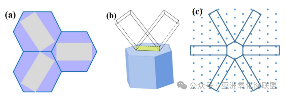
Figure 1. Schematic illustration of the sixfold rotational domain structure of β-Ga₂O₃ grown on sapphire caused by the threefold rotational symmetry of sapphire and the twofold rotational symmetry of β-Ga₂O₃.
To suppress the sixfold domain structure of β-Ga₂O₃, our team introduced miscut sapphire substrates (Figure 2), which effectively break the in-plane symmetry of the sapphire c-plane. The atomic steps on the miscut sapphire surface serve as preferential bonding sites for adatoms, promoting the preferred orientation of β-Ga₂O₃ crystalline domains and improving the crystalline quality of the film. Based on the atomic arrangement of the sapphire c-plane (Figure 3), a 6° miscut toward the m-plane was selected as the optimal orientation. This configuration significantly increases the step density, further suppresses random nucleation, and reduces the full width at half maximum (FWHM) of the rocking curve for the Ga₂O₃ (-201) plane from 1.3° to 0.6°.
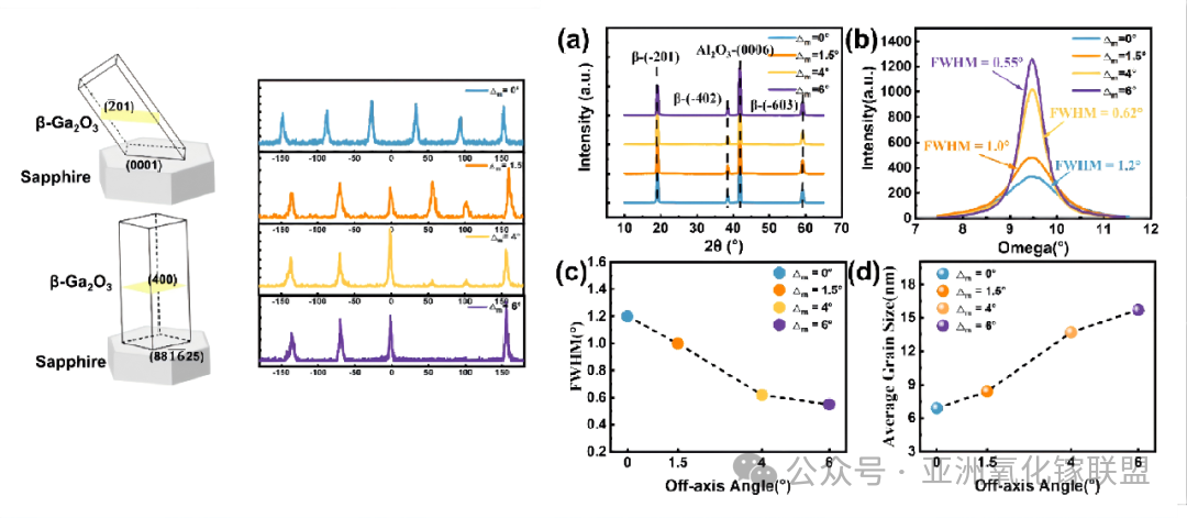
Figure 2. Suppression of sixfold domains in β-Ga₂O₃ using sapphire substrates with different miscut angles and the corresponding XRD characterization results.
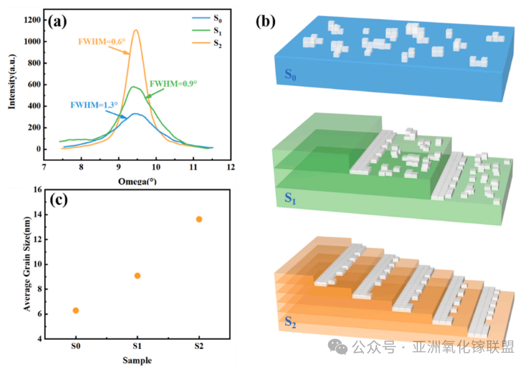
Figure 3. Influence of step-terrace width on miscut sapphire substrates on the crystalline quality of β-Ga₂O₃ films.
In addition, the team proposed a nanoparticle-assisted epitaxy technique to further promote lateral coalescence of the film (Figure 4). By controlling the MOCVD epitaxial growth parameters, Ga droplets were deposited on the miscut sapphire substrate and thermally oxidized to form Ga₂O₃ single-crystal nanoparticles. These nanoparticles serve as nucleation sites for subsequent film growth, thereby facilitating lateral merging of the film and significantly reducing the dislocation density. As a result, the FWHM of the rocking curve for the (-201) plane of a 270-nm-thick β-Ga₂O₃ film was further reduced to 0.48°. Based on this structure, MSM solar-blind ultraviolet photodetectors were fabricated, showing significantly improved performance. At -5 V, the dark current decreased from 0.389 μA to 81.03 pA, and the response speed improved from 258/1690 μs to 62/142 μs. The device also achieved a high responsivity of 43.5 A/W, a detectivity of 2.81 × 10¹⁴ Jones, and a linear dynamic range of 61 dB. Mechanistically, cathodoluminescence measurements indicate that the NPSL structure effectively suppresses deep-level defects such as self-trapped holes and increases the Schottky barrier height. Although part of the photoconductive gain is sacrificed, the device obtains lower dark current, faster response, and improved linearity.
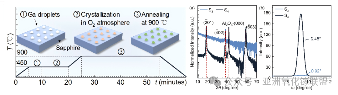
Figure 4. Nanoparticle-assisted epitaxial growth of Ga₂O₃ films and corresponding XRD results.
Since p-type Ga₂O₃ remains difficult to achieve, conventional Ga₂O₃ ultraviolet photodetectors typically rely on external bias voltage to separate photogenerated carriers, resulting in system complexity and higher power consumption [5,6]. To realize self-powered (0 V) high-performance ultraviolet detection, the team first grew p-GaN layers on sapphire substrates [7-9] (Figure 5). By tuning the MOCVD growth temperature, α-, κ-, κ/β-, and β-Ga₂O₃ films were epitaxially grown on the p-GaN layer, and the influence of different crystal phases on device performance was systematically compared. Meanwhile, in-situ annealing at 750 °C in an O₂ atmosphere was performed on the p-GaN surface to form an ultrathin GaON dielectric layer, which was used to suppress the persistent photoconductivity (PPC) effect caused by defects. This strategy significantly enhanced self-powered detection performance at 0 V while maintaining millisecond-level response dynamics. The results show that the responsivity of the β-Ga₂O₃/p-GaN heterostructure at 0 V increased by approximately 20 times. The self-powered β-Ga₂O₃/p-GaN detector exhibited an ultralow dark current of 3.08 pA, along with high responsivities of 3.8 A/W at 254 nm and 0.83 A/W at 365 nm. These results confirm that crystal phase engineering combined with in-situ GaON interface engineering can significantly enhance the performance of self-powered Ga₂O₃/p-GaN ultraviolet photodetectors (Figure 6).
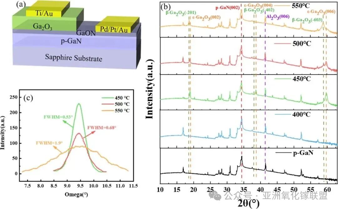
Figure 5. Influence of growth temperature on β-Ga₂O₃ epitaxy on p-GaN.
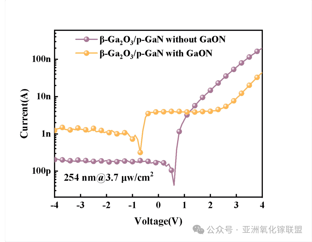
Figure 6. I–V characteristics of β-Ga₂O₃/p-GaN heterojunctions with and without the GaON interfacial layer.
Sapphire and α-Ga₂O₃ both belong to the R-3c space group, exhibiting identical symmetry. The lattice mismatch between m-plane sapphire and α-Ga₂O₃ along the [0006] direction is only 3.3%. However, since the α phase is metastable, β-phase mixing can easily occur during growth, which severely degrades film quality. To address this issue, our team investigated the thermodynamic nucleation and surface kinetic mechanisms of α-Ga₂O₃ heteroepitaxy on m-plane sapphire using the MOCVD method. The study revealed that the film crystal phase is governed by the combined effects of phase stability, interfacial energy, and supersaturation. During growth, screw dislocations propagating to the surface induce β-phase transformation, leading to a layer-plus-island growth mode, which results in relatively high surface roughness. Based on these findings, as shown in Figure 7, the team developed a high-temperature AlₓGa₁₋ₓO buffer layer technology. This buffer layer effectively alleviates the lattice mismatch between the film and the substrate, while regulating film stress states and the motion of screw dislocations, thereby suppressing island-like protrusions and improving the surface morphology.Ultimately, high-quality heteroepitaxial α-Ga₂O₃ films were achieved, with a rocking curve FWHM of 0.26° for the (30-30) plane and 0.38° for the asymmetric (10-14) plane, and a surface roughness of 2.45 nm. These results lay the foundation for low-cost heteroepitaxial α-Ga₂O₃ power device fabrication.
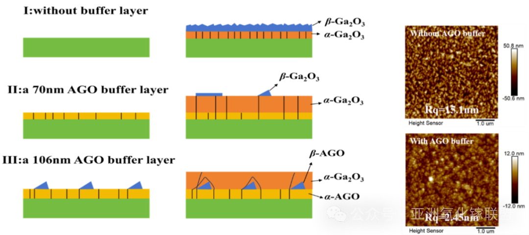
Figure 7. Nucleation mechanism and surface morphology of heteroepitaxial α-Ga₂O₃ films.
2.Heteroepitaxial Growth of Gallium Oxide on Silicon Substrates
Silicon substrates, owing to their low fabrication cost, large wafer size, and strong compatibility with CMOS processes, are considered one of the most promising substrates for Ga₂O₃ epitaxial growth. However, achieving high-quality Ga₂O₃ films on Si substrates remains challenging.
First, during the epitaxial growth of Ga₂O₃, the high-temperature oxygen environment can oxidize the Si substrate, forming an amorphous SiOₓ interfacial layer. This degrades the nucleation quality in the initial growth stage and may lead to the formation of amorphous or polycrystalline Ga₂O₃ structures. Second, the large lattice mismatch and thermal expansion mismatch between Ga₂O₃ and Si substrates result in an extremely high density of defects in the grown Ga₂O₃ films.
To address these key issues, our team proposed and established several parallel buffer-layer engineering strategies, including Al₂O₃ buffer layers, AlN buffer layers, and metallic Mo buffer layers. The core design objective of these buffer layers is to construct an intermediate interface between the Si substrate and the Ga₂O₃ film that can simultaneously suppress oxidation, alleviate lattice and thermal mismatch, and regulate nucleation behavior, thereby enabling the growth of high-quality Ga₂O₃ films.
First, based on Si(111) substrates, the team introduced a high-resistivity amorphous Al₂O₃ buffer layer grown by PEALD (Figure 8). This buffer layer effectively mitigates the epitaxial stress and defect formation caused by the significant lattice-constant mismatch and thermal expansion mismatch between Si and Ga₂O₃. Meanwhile, the high-resistivity amorphous Al₂O₃ layer serves as an interfacial isolation and passivation layer, suppressing interfacial reactions and preventing the formation of an amorphous SiO₂ oxidation layer. As a result, the defect density of the Ga₂O₃ films is reduced and the surface morphology is improved.
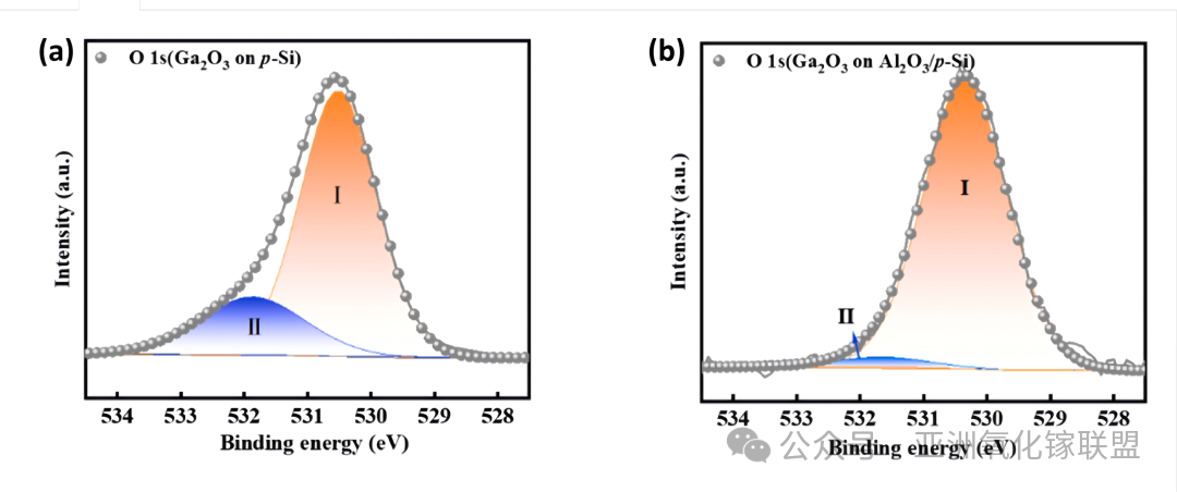
Figure 8. XPS characterization results of Ga₂O₃ films grown with and without an Al₂O₃ buffer layer.
On this basis, the team fabricated and characterized quasi-vertical ultraviolet photodetectors (Figure 9). Compared with Ga₂O₃/p-Si devices, the Ga₂O₃/Al₂O₃/Si devices exhibit significantly improved performance under 254 nm illumination, including an ultralow dark current of 99.4 pA, a photo-to-dark current ratio exceeding 10⁴, a responsivity of 8.1 A/W at a fixed bias of 10 V, and faster photoresponse speeds (rise and decay times of 0.89 s and 0.29 s, respectively). These results demonstrate that Al₂O₃ not only improves epitaxial quality as a buffer layer, but also functions as an electron-blocking layer, optimizing carrier transport across the heterojunction while suppressing leakage current. This approach provides a practical pathway for constructing low-leakage, array-compatible, and integrable solar-blind ultraviolet photodetector platforms on low-cost Si substrates.
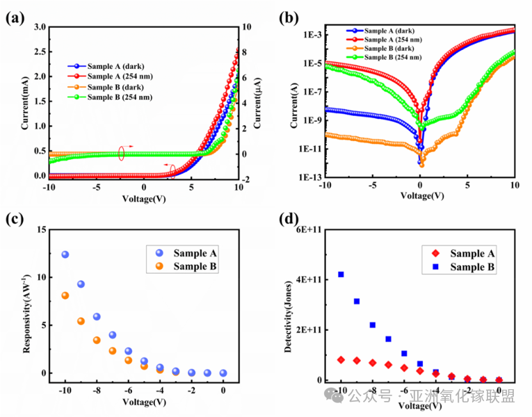
Figure 9. Performance comparison between Ga₂O₃/p-Si and Ga₂O₃/Al₂O₃/Si photodetectors.
Building on this work, the team further developed an AlN buffer-layer technology (Figures 10 and 11). The lattice mismatch between AlN and Ga₂O₃ is only about 6.4%, and the AlN buffer layer can also effectively suppress oxidation of the Si substrate during high-temperature epitaxial growth. By investigating the influence of growth temperature on the phase transition of gallium oxide, the team identified the epitaxial growth temperature window for κ-Ga₂O₃ films. To further improve crystal quality, key MOCVD growth parameters—including the O/Ga ratio and chamber pressure—were systematically optimized to precisely control both the lateral and vertical growth rates of the film. This process promotes lateral coalescence of three-dimensional island grains and dislocation annihilation.
At a growth temperature of 500 °C, the FWHM of the rocking curve for the κ-Ga₂O₃ (002) plane reached 0.68°, with a surface roughness (Ra) of only 0.64 nm, while the uniformity of 4-inch Si-based κ-Ga₂O₃ films reached 98.2%.
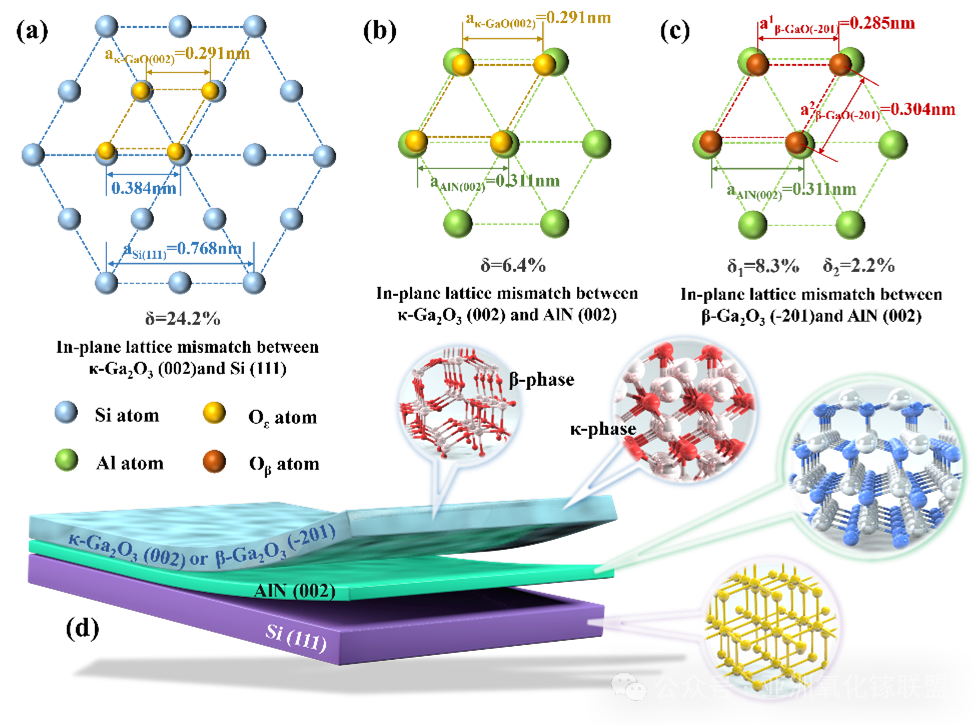
Figure 10. Schematic illustration of lattice mismatch between the Si(111) substrate and Ga₂O₃ films.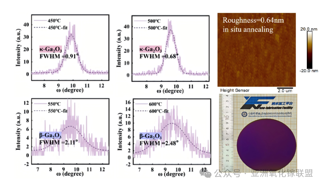
Figure 11. Growth results of Ga₂O₃ films on Si substrates.
In addition, the team proposed an epitaxial strategy introducing a Mo metallic insertion layer on Si(100) substrates [14] (Figure 12), enabling the heteroepitaxial growth of Ga₂O₃ films and the fabrication of quasi-vertical solar-blind ultraviolet photodetectors. The Mo insertion layer serves two important roles. First, it acts as a transition buffer layer, effectively mitigating nucleation and defect issues caused by large lattice mismatch during heteroepitaxy and thereby improving film crystallinity. Second, Mo has a relatively low work function, enabling the formation of a good ohmic contact with Ga₂O₃, which simplifies device design and fabrication.
In terms of device architecture, the quasi-vertical structure allows the electrode spacing to be precisely controlled through the film thickness. By reducing the film thickness, the carrier transit distance is shortened, thereby reducing transit-time limitations on transient response and improving device speed. As shown in Figure 13, the final device achieved a response time of 22 ms and a responsivity of 243.14 A/W.
The Mo metallic buffer layer therefore not only provides an effective pathway for achieving high-quality Ga₂O₃ epitaxy on Si substrates, but also introduces new design flexibility for device architecture and fabrication processes.
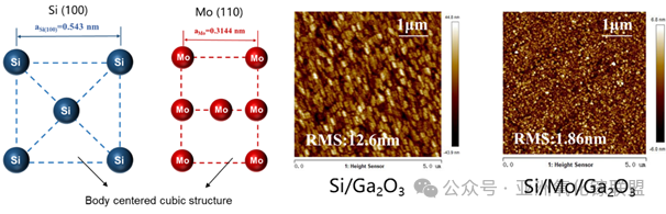
Figure 12. Atomic structures of Si(100) and Mo(100) surfaces and comparison of Ga₂O₃ surface morphology with and without a Mo insertion layer.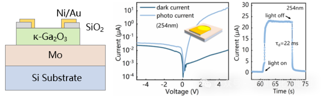
Figure 13. Schematic diagram of the quasi-vertical SBD device structure and its performance characterization.
3.Epitaxial Growth of Ga₂O₃ Nanowires on Sapphire Substrates
β-Ga₂O₃ nanowires possess a higher specific surface area, providing richer surface states at the interface and enhancing interactions with the surrounding environment. In addition, their one-dimensional carrier transport channels make them widely studied for applications in nano field-effect transistors (FETs), gas sensors, and solar-blind ultraviolet photodetectors. For large-scale integrated circuit applications, structural consistency and orientation uniformity of nanowires are crucial; therefore, achieving controllable growth of nanowire arrays becomes a key challenge. The team first employed MOCVD technology to grow self-catalyzed vertical β-Ga₂O₃ nanowire arrays on c-plane GaN substrates(Fig. 14), establishing a stable vapor transport and reaction environment under relatively low reaction pressure. Key parameters such as growth temperature and Ga/O ratio were optimized to achieve a controllable growth window with a high vertical alignment ratio and uniform orientation. Meanwhile, to address common issues in nanowire growth—including bending, abnormal morphology, and array non-uniformity—the team proposed a simplified coalescence model based on reduced cluster mobility. During different growth stages, the stability of catalytic droplets, surface diffusion, and supply competition collectively influence the axial-to-radial growth ratio and morphological evolution of nanowires. This work provides a clear mechanistic basis for further achieving ordered arrays, improving uniformity, and enabling device integration of nanowires.
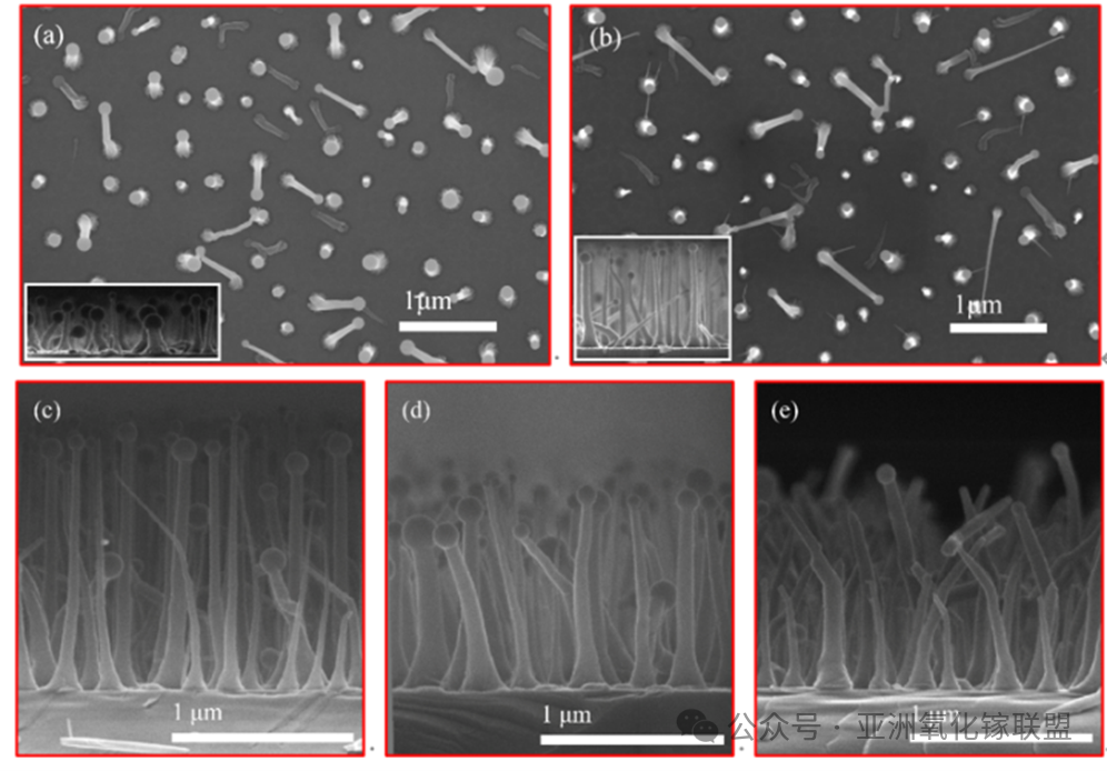
Fig. 14 SEM images of random β-Ga₂O₃ nanowire arrays under different growth conditions
Subsequently, the team further investigated the effects of Ga metal catalyst deposition time and annealing processes on random nanowire arrays (Fig. 15). During the growth of random nanowire arrays, the array density and uniformity are typically dominated by the density, size, and spatial distribution of Ga catalytic droplets. However, simply increasing the deposition amount usually changes both droplet density and droplet diameter simultaneously. Larger droplets may enhance coalescence and alter migration behavior, thereby influencing the final nanowire density and size distribution. To address this issue, the team fixed the annealing conditions (650 °C, 1.5 min) to stabilize droplet size during annealing, while adjusting the Ga pre-deposition time to independently control droplet density and average spacing, thereby regulating the spatial distribution of catalysts. Experimental results show that under identical catalyst deposition and annealing conditions, Ga droplets exhibit significant differences on different surfaces: the catalyst density is approximately 6.2 droplets/μm² on GaN surfaces but about 2.5 droplets/μm² on SiO₂ surfaces. Meanwhile, the migration distance of Ga droplets ranges from approximately 680 nm to 1.4 μm on GaN, whereas it can reach 500 nm to 3 μm on SiO₂, demonstrating that differences in surface migration rates between substrates or mask materials play a decisive role in catalyst distribution and the resulting nanowire arrays. Based on this observation, the team designed a SiO₂ mask with ordered nanopore arrays (200 nm pore diameter, 500 nm period) to control catalyst deposition. Under appropriate catalyst deposition and annealing conditions, no excess Ga droplets were observed on the mask surface, while each nanopore contained a single droplet without obvious overflow. A nanopore array with a 100% filling rate was achieved, enabling the fabrication of vertically aligned and ordered β-Ga₂O₃ nanowire arrays perpendicular to the substrate.
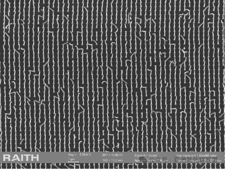
Fig. 15 Model schematic of In-assisted epitaxial growth of β-Ga₂O₃ thin films and comparison of surface morphology with and without In-assisted growth
4.Homoepitaxial Growth of β-Ga₂O₃ Thin Films
Currently, β-Ga₂O₃ free-standing single-crystal substrates can reach wafer sizes of up to 8 inches. However, homoepitaxial growth of β-Ga₂O₃ thin films still faces challenges such as slow growth rates, stripe-like trench morphologies, and high surface roughness. These issues are related to the desorption of suboxide Ga₂O and the anisotropy of the Ga₂O₃ surface energy. During epitaxial growth, Ga atoms react with deposited Ga₂O₃, producing gaseous Ga₂O (reactions (1) and (2)). Film growth and etching reactions compete simultaneously. The anisotropy in surface energy and atomic diffusion capability leads to the formation of stripe-like trenches along the [010] direction, resulting in pronounced surface undulations and significantly increased roughness. In addition, n-type doping of β-Ga₂O₃ films remains limited. High doping concentrations, typically required to realize Ohmic contacts, are often achieved through high-dose Si ion implantation, which introduces substantial damage. Therefore, regulating the growth mode of β-Ga₂O₃ films and achieving controllable in-situ Si doping are of great significance.
To suppress the trench-like surface morphology of β-Ga₂O₃ homoepitaxial films, the team introduced a metal-organic precursor of In into the MOCVD system as a surfactant-assisted epitaxy source (Fig. 16). During atomic deposition, InGaO species with higher desorption energy are formed (Ga₂O: 3.38 eV; InGaO: 3.7 eV), which suppress the desorption of Ga₂O and thereby increase the growth rate of β-Ga₂O₃ films. Meanwhile, introducing In during growth promotes a two-dimensional layer-by-layer growth mode, stabilizes surface thermal fluctuations, and eliminates the trench morphology typically observed in conventional epitaxy, resulting in relatively smooth β-Ga₂O₃ homoepitaxial films. The surface roughness is significantly reduced from 24.7 nm to 2.2 nm. The In-assisted epitaxy method may also generate small amounts of In₂O₃, which has a relatively narrow thermal stability window. However, because β-Ga₂O₃ has a lower Gibbs free energy (ΔGf β-Ga₂O₃ = −998.3 kJ/mol; ΔGf In₂O₃ = −830.7 kJ/mol), it is thermodynamically more stable. During growth, Ga atoms can replace In in In₂O₃ through substitution reactions (reaction (4)), removing most In impurities from the film and thereby improving film purity. SIMS and HRXRD measurements further show that the In concentration in the film is approximately 7.05 × 10¹⁶ cm⁻³, with higher concentration only near the interface due to elemental accumulation, and thus it does not significantly affect the rocking curve full width at half maximum.
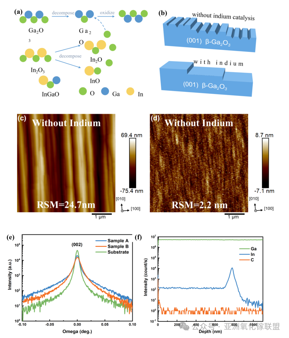
Fig. 16 Schematic model of In-assisted β-Ga₂O₃ epitaxy and characterization comparison of films with and without In-assisted growth
Based on this epitaxial process, the team further investigated controllable n-type doping of β-Ga₂O₃ homoepitaxial films [29]. Si donor doping was introduced in situ by supplying SiH₄ into the MOCVD chamber. It was found that the introduction of an appropriate amount of SiH₄ significantly alters the growth mode of β-Ga₂O₃ films. As shown in Fig. 17, when Si atoms enter the β-Ga₂O₃ growth system, they randomly nucleate on the material surface, and Ga adatoms diffuse laterally around the Si nucleation sites and merge within the two-dimensional island plane. This process competes with the vertical stacking growth of adatoms, suppressing the growth of three-dimensional islands and eliminating void morphologies caused by insufficient lateral migration, thereby improving the film surface morphology. When the SiH₄ molar flow rate corresponds to a doping concentration of 2 × 10¹⁷ cm⁻³, the surface roughness of β-Ga₂O₃ decreases to 1.07 nm.
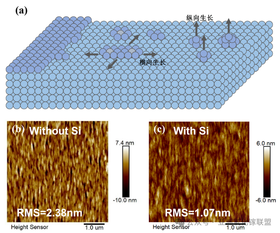
Fig. 17 Schematic model of Si-doped β-Ga₂O₃ film growth and comparison of surface morphology with and without Si-doped epitaxy
After further optimization of growth and doping conditions, the doped samples were activated by in-situ annealing and characterized by C–V and SIMS measurements, as shown in Fig. 18. The n-type carrier concentration of doped β-Ga₂O₃ films can be controllably tuned within the range of 10¹⁵–10²⁰ cm⁻³, with a Si donor activation efficiency exceeding 60%. For epitaxial films with a doping concentration of 1.64 × 10²⁰ cm⁻³, 50 nm and 100 nm Ti/Au metals were deposited on the film surface by electron-beam evaporation. After annealing at 475 °C for 1 min in an N₂ atmosphere to form Ohmic contacts, electrical measurements show that the β-Ga₂O₃ films exhibit excellent Ohmic contact characteristics, with a contact resistance of 3.73 Ω·mm, a sheet resistance of 1084 Ω/□, and a specific contact resistivity as low as 1.29 × 10⁻⁴ Ω·cm². These electrical properties are comparable to those of Si-implanted samples, demonstrating that controllable and effective Si doping has been achieved in β-Ga₂O₃ films. Finally, van der Pauw Hall measurements reveal a carrier mobility of 74.6 cm²/V·s, meeting the requirements for the fabrication of lateral enhancement-mode and depletion-mode power devices.
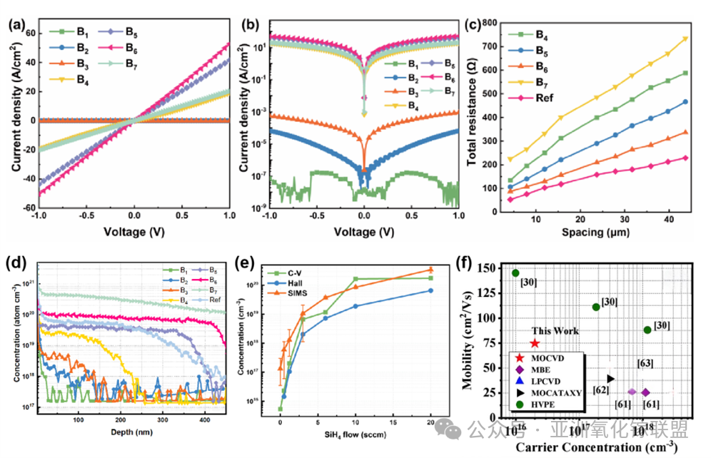
Fig. 18 Electrical properties of Si-doped β-Ga₂O₃ thin films
Introduction to Epitaxy-Related Equipment
Since its establishment, the Nanofabrication Platform has placed strong emphasis on compound semiconductor material epitaxy and device research and development. The platform is equipped with multiple internationally advanced commercial MOCVD systems for wide-bandgap semiconductor epitaxy, including systems from AIXTRON (Germany) and TAIYO NIPPON SANSO (Japan) for III-nitride and III-oxide compound semiconductors, as well as an MPCVD system for diamond epitaxial growth. In addition, the platform is equipped with a range of material characterization and testing instruments, including a high-resolution X-ray diffractometer (HRXRD), scanning electron microscope (SEM), atomic force microscope (AFM), optical microscope, and Hall measurement system. These facilities enable the complete semiconductor chip fabrication workflow within the platform’s cleanroom environment, covering epitaxial growth, material characterization and testing, and device fabrication.

Fig. 19 Overview of growth and characterization equipment on the processing platform
Contract Processing and Technical Collaboration
The Nanofabrication Platform operates as an open public service platform and welcomes outstanding research teams from enterprises, universities, and research institutes to collaborate and exchange ideas. We provide contract processing services for a variety of wide-bandgap semiconductor materials and device structures, and we also look forward to collaborating with partners on diverse research and development projects.
Representative Publications:
[1] Ma Y J, et al. High-performance β-Ga2O3 solar blind ultraviolet photodetectors epitaxially grown on (110) TiO2 substrates by metalorganic chemical vapor deposition [J]. Vacuum, 2021, 191: 110402.
[2] Ma Y J, et al. Effect of off-axis substrate angles on β-Ga2O3 thin films and solar-blind ultraviolet photodetectors grown on sapphire by MOCVD [J]. Materials Science in Semiconductor Processing, 2021, 131: 105856.
[3] Ma Y J, et al. Mis-cut direction of substrate effect on the photoresponse characteristic of β-Ga2O3 film [J]. Vacuum, 2022, 198: 110886.
[4] Chen T W, et al. High-speed and ultrasensitive solar-blind ultraviolet photodetectors based on in situ grown β-Ga2O3 single-crystal films [J]. ACS Applied Materials & Interfaces, 2024, 16(5):6068-6077.
[5] He T, et al. Metalorganic chemical vapor deposition heteroepitaxial β-Ga2O3 and black phosphorus p-n heterojunction for solar-blind ultraviolet and infrared dual-band photodetector [J]. Physica Status Solidi A–Applications and Materials Science, 2020, 217: 1900861.
[6] Chen T W, et al. Ultrahigh responsivity β-Ga2O3/BP junction field effect phototransistors for UV/IR dual-band detection [J]. IEEE Sensors Journal, 2023, 14(14):15504-15511.
[7] Ma Y J, et al. High photoresponsivity self-powered a-, ε-, and β-Ga2O3 /p-GaN heterojunction UV photodetectors with an in-situ GaON layer by MOCVD [J]. ACS Applied Materials & Interfaces, 2022, 14(30): 35194-35204.
[8] Chen T W, et al. Self‐powered and spectrally distinctive nanoporous Ga2O3/GaN epitaxial heterojunction ultraviolet photodetectors [J]. Advanced Photonics Research, 2021, 2(8): 2100049.
[9] Zhou X, et al. Band alignment of ultrawide bandgap ε-Ga2O3/h-BCN heterojunction epitaxially grown by metalorganic chemical vapor deposition [J]. Applied Surface Science, 2022, 583: 152502.
[10] Li Z C, et al. Improving the quality of MOCVD-Grown α-Ga2O3 by introducing an AGO buffer on m-plane sapphire [J]. Vacuum, 2025, 240: 114445.
[11] Li Z C, et al. Suppression of screw dislocation-Induced Hillocks in MOCVD-Grown α-Ga2O3 on m-plane sapphire by introducing a high-temperature buffer [J]. Crystal Growth & Design, 2025, 25(5): 1406-1414.
[12] Qian H, et al. Quasi-vertical ε-Ga2O3 solar-blind photodetectors grown on p-Si substrates with Al2O3 buffer layer by metalorganic chemical vapor deposition [J]. Vacuum, 2022, 200: 111019.
[13] Hu Y, et al High-performance ε-Ga2O3 solar-blind ultraviolet photodetectors on Si (100) substrate with molybdenum buffer layer [J]. Vacuum, 2023, 213: 112130.
[14] Hu Y, et al. Effects of growth temperature on phase transformation and crystal quality of Ga2O3 films grown on Si/AlN composite substrates by MOCVD [J]. Materials Science in Semiconductor Processing, 2024, 178: 108453.
[15] Hu Y, et al. Wafer-scale high-performance flexible solar-blind ultraviolet photodetectors based on a-Ga2O3 grown by MOCVD [J]. Journal of Materials Science & Technology, 2026, 259: 188–196.
[16] Chen T W, et al. Ultrasensitive dynamic ultraviolet imaging based on a Ga2O3 photodetector array [J]. Optics Letters, 2025, 50(5):1633-1636.
[17] Zhang H Y, et al. High-speed and high-responsivity quasi-vertical Schottky photodetectors of epitaxial Ga2O3 on Pt substrate [J]. IEEE Electron Device Letters, 2025, 46(1): 60-63.
[18] Cao X, et al. Controllable Ga catalyst deposition on GaN template and fabrication of ordered vertical β-Ga2O3 nanowire array [J]. Journal of Physics D: Applied Physics, 2020, 53(30).
[19] Zeng C H, et al Solar-blind ultraviolet detector based on ordered nanoporous β-Ga2O3 film [J]. Japanese Journal of Applied Physics, 2022, 61(4): 042004.
[20] Ma Y J, et al. Controlled lateral epitaxial growth in vertical β-Ga2O3 nanowires on sapphire by MOCVD [J]. Journal of Physics D: Applied Physics, 2021, 54: 305101.
[21] Zhou X, et al. Ultrahigh responsivity deep-ultraviolet ε-Ga2O3 field effect phototransistors with P-Si gate [J]. Journal of Physics D: Applied Physics, 2021, 54(44): 445103.
[22] Zeng C H, et al. Ultraviolet photodetector based on vertical β-Ga2O3 nanowire array on GaN substrate [J]. Materials Research Express, 2021, 8(5): 055903.
[23] Cao X, et al. Crystalline properties of ε-Ga2O3 film grown on c-sapphire by MOCVD and solar-blind ultraviolet photodetector [J]. Materials Science in Semiconductor Processing, 2021, 123: 105532.
[24] Li J S, et al. Self-catalyzed metal organic chemical vapor deposition growth of vertical β-Ga2O3 nanowire arrays [J]. Nanotechnology, 2020, 31: 02LT01.
[25] Li B T, et al. A comprehensive review of recent progress on enhancement-mode β-Ga2O3 FETs: Growth, devices and properties [J]. Journal of Semiconductors, 2023, 44(6): 061801.
[26] ] Bian C X, et al. Effect of RF power and gas ratio on the sidewall of β-Ga2O3 films via inductively coupled plasma etching [J]. Japanese Journal of Applied Physics, 2023, 62(1): 011004.
[27] Feng B Y, et al. The effect of annealing on the Sn-doped (−201) β-Ga2O3 bulk [J]. Materials Science in Semiconductor Processing, 2022, 147: 106752.
[28] Tang W B, et al. High-quality (001) β-Ga2O3 homoepitaxial growth by metalorganic chemical vapor deposition enabled by in situ indium surfactant [J]. Applied Physics Letters, 2022, 120(21): 212103.
[29] Tang W B, et al. Homoepitaxial growth of (100) Si-doped β-Ga2O3 films via MOCVD [J]. Journal of Semiconductors, 2023, 44(6): 062801.
[30] Li B T, et al. Enhancement-mode Ga2O3 FETs with an unintentionally doped (001) β-Ga2O3 channel layer grown by metal organic chemical vapor deposition [J]. Japanese Journal of Applied Physics, 2024, 6
