Paper Sharing
【Member Papers】Solar‐Blind Enhanced Dual‐Band Ultraviolet Photodetector
日期:2026-03-13阅读:307
Researchers from Northeast Normal University have published a dissertation titled "Solar‐Blind Enhanced Dual‐Band Ultraviolet Photodetector" in Small.
Background
Ultraviolet (UV) detection is a widely used optical detection technology with important applications in secure communication, corona monitoring, flame detection, biochemical analysis, and space exploration. Currently, the main commercial UV photodetectors are photomultiplier tubes (PMTs) and silicon-based photodiodes. PMTs have the advantages of high speed and high sensitivity but suffer from large size, fragility, and high operating voltage. In contrast, silicon-based photodiodes are small, low-power, and low-cost, yet require additional filter modules for UV detection due to their small bandgap, and exhibit low sensitivity in the UV range due to indirect bandgap characteristics.
Wide-bandgap semiconductors are ideal for UV detection due to their suitable bandgap, high UV absorption coefficient, and good thermal stability. Among them, gallium oxide (Ga₂O₃) with a bandgap of ~4.9 eV has a natural photoresponse in the solar-blind UV region (200–280 nm), and also features excellent thermal and chemical stability as well as a high absorption coefficient for solar-blind UV, making it the most promising material for solar-blind UV detectors.
However, current Ga₂O₃-based UV photodetectors face two major challenges: low responsivity to solar-blind UV light (the peak responsivity of commercial detectors is mostly outside the solar-blind band), and the significant persistent photoconductivity (PPC) effect which degrades the device response speed. In addition, most reported detectors only enable single-band or broadband detection and cannot effectively distinguish UV light of different wavelengths. Ternary alloy wide-bandgap materials tend to have degraded quality with increased alloying, while diamond is more suitable for power devices than photodetection. To address these issues, this study reports the design and fabrication of a β-Ga₂O₃/(AlₓGa₁₋ₓ)₂O₃/GaN heterojunction dual-band UV photodetector. The (AlₓGa₁₋ₓ)₂O₃ barrier layer is introduced to suppress reverse leakage current, and self-trapped holes (STHs) in Ga₂O₃ induce carrier tunneling to achieve solar-blind UV photocurrent gain. Meanwhile, the discrimination between solar-blind UV (λ≤270 nm) and long-wave UV (λ>270 nm) is realized by the difference in current relaxation rates after illumination with different wavelengths.
Abstract
A solar-blind enhanced dual-band UV photodetector based on β-Ga₂O₃/(AlₓGa₁₋ₓ)₂O₃/GaN nBp heterojunction was fabricated by metal-organic chemical vapor deposition (MOCVD), with a 250 nm-thick Ga₂O₃ layer, two thicknesses of (AlₓGa₁₋ₓ)₂O₃ barrier layer (30 nm for S2# and 60 nm for S3#), and an effective light-receiving area of 0.3 cm².
The introduction of the (AlₓGa₁₋ₓ)₂O₃ barrier layer reduces the reverse leakage current of the heterojunction by more than six orders of magnitude (at -10 V bias), significantly improving the dark state performance of the device. Under solar-blind UV illumination, self-trapped holes (STHs) generated in Ga₂O₃ enhance the junction electric field and induce carrier tunneling, achieving photocurrent gain. The device exhibits excellent solar-blind UV detection performance at -20 V bias: a photocurrent gain of 2033, a responsivity of 900 A/W, and a detectivity of 2.55×10¹³ Jones.
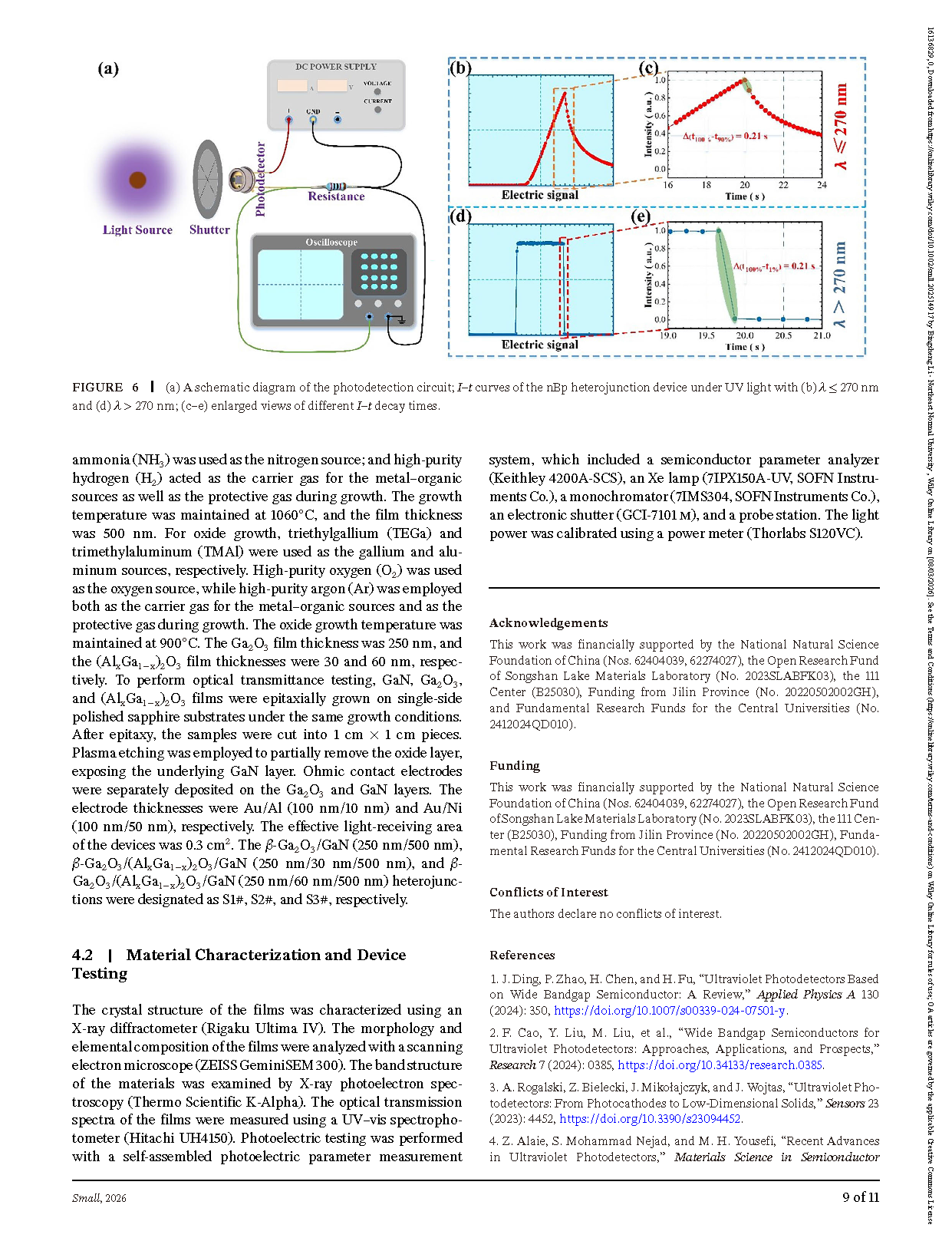
To suppress the persistent photoconductivity (PPC) effect under solar-blind UV illumination, a method of ultraviolet illumination combined with circuit interruption was adopted, which significantly shortens the current relaxation time—the current can drop from the maximum value to the baseline by five orders of magnitude within 3 seconds. In addition, a novel dual-band UV detection method was proposed by utilizing the difference in current relaxation rates of the device under UV illumination of different wavelengths: the current only drops from 100% to 90% within 210 ms after 250 nm solar-blind UV illumination, while it drops from 100% to 1% within the same time after 350 nm long-wave UV illumination, thus enabling effective discrimination between solar-blind and long-wave UV light.
Highlights
● A solar-blind enhanced dual-band UV photodetector based on β-Ga₂O₃/(AlₓGa₁₋ₓ)₂O₃/GaN heterojunction is developed.
● The introduction of (AlₓGa₁₋ₓ)₂O₃ barrier layer reduces the reverse leakage current of the device by more than six orders of magnitude, significantly optimizing the dark state performance.
● A high photocurrent gain of 2033 is achieved by utilizing the carrier tunneling effect induced by self-trapped holes in Ga₂O₃ under solar-blind UV illumination.
● The device achieves a high responsivity of 900 A/W and a high detectivity of 2.55×10¹³ Jones at -20 V bias, with excellent solar-blind UV detection performance.
● A method of ultraviolet illumination combined with circuit interruption is proposed to effectively suppress the persistent photoconductivity effect and significantly shorten the current relaxation time.
● The precise discrimination between solar-blind UV (λ≤270 nm) and long-wave UV (λ>270 nm) is realized by the difference in current relaxation rates after irradiation with different wavelengths of UV light.
Conclusion
The β-Ga₂O₃/(AlₓGa₁₋ₓ)₂O₃/GaN nBp heterojunction photodetector fabricated in this study successfully achieves solar-blind enhanced dual-band UV detection. The introduction of the (AlₓGa₁₋ₓ)₂O₃ barrier layer effectively suppresses the reverse leakage current of the device and improves the dark state working performance. Under solar-blind UV illumination, self-trapped holes generated in Ga₂O₃ enhance the junction electric field and induce carrier tunneling, enabling the device to obtain a photocurrent gain of 2033, a solar-blind UV responsivity of 900 A/W, and a detectivity of 2.55×10¹³ Jones at -20 V bias, with a significant improvement in solar-blind UV detection performance.
Experiments confirm that the combination of illumination and electric field variation can significantly accelerate the current relaxation speed of the device after solar-blind UV irradiation and effectively suppress the persistent photoconductivity effect. In addition, the discrimination and detection of UV light with different wavelengths can be realized by utilizing the difference in relaxation time of the device after illumination in different bands, providing a new implementation idea for dual-band UV detection technology. The photodetector has both high-sensitivity solar-blind UV detection and dual-band discrimination capabilities, and has important application potential in UV detection, environmental monitoring, space exploration and other fields.
Project Support
This work was financially supported by the National Natural Science Foundation of China (Grant Nos. 62404039, 62274027), the Open Research Fund of Songshan Lake Materials Laboratory (Grant No. 2023SLABFK03), the 111 Center (Grant No. B25030), Funding from Jilin Province (Grant No. 20220502002GH), and Fundamental Research Funds for the Central Universities (Grant No. 2412024QD010).
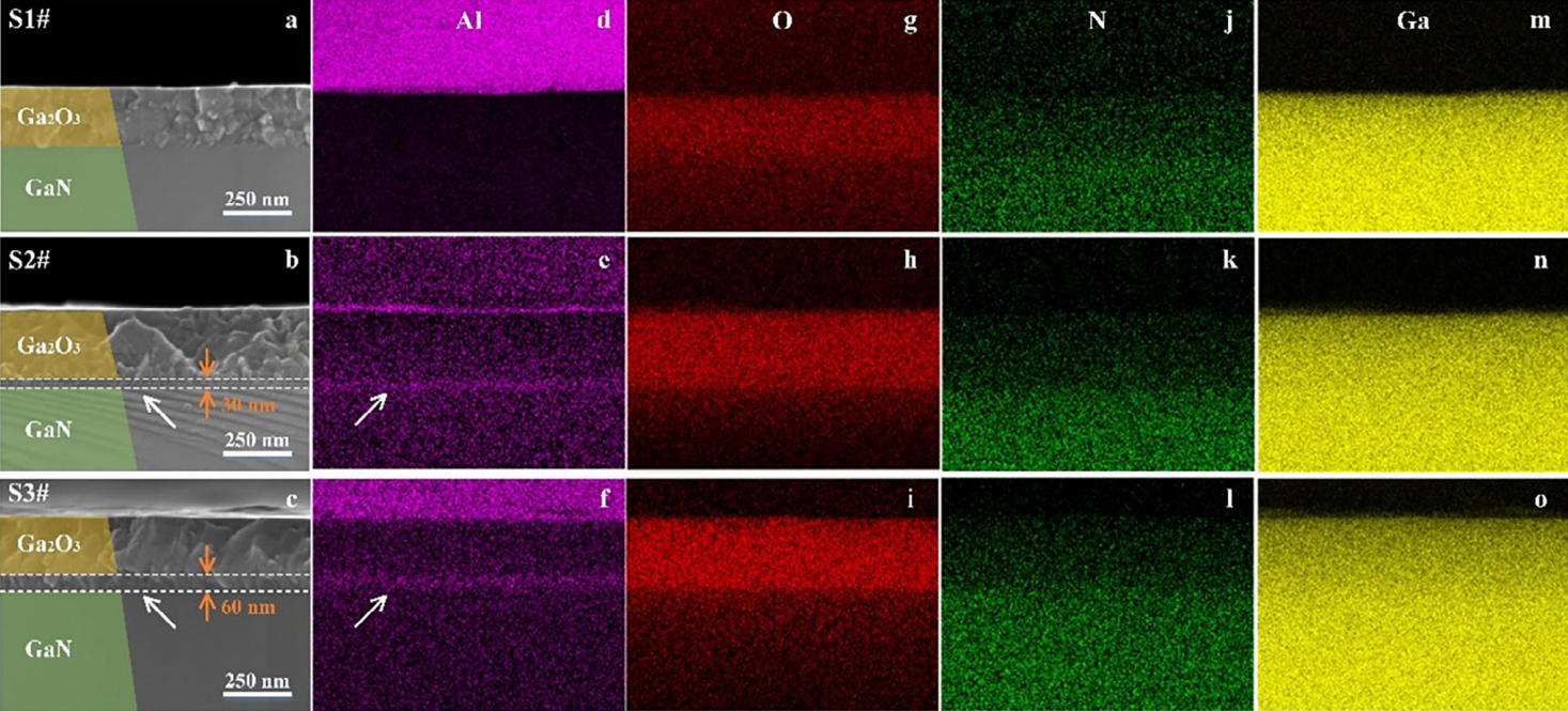
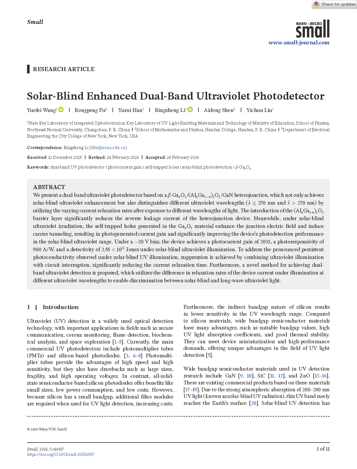
Fig. 1. (a–c) Cross-sectional scanning electron microscope images of different heterojunctions, elemental distribution maps of (d–f) Al, (g–i)O, (j–l) N, and (m–o) Ga.
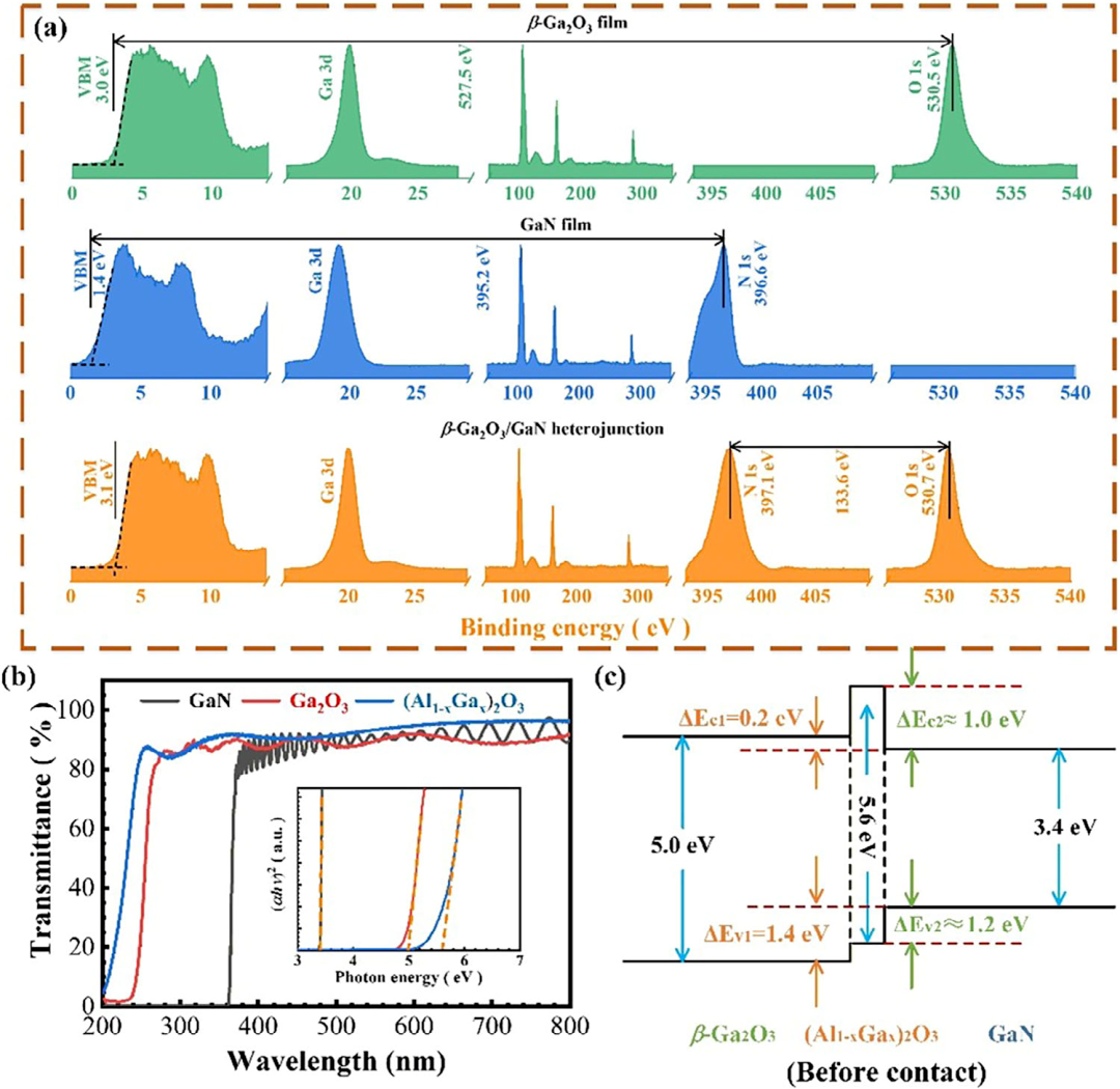
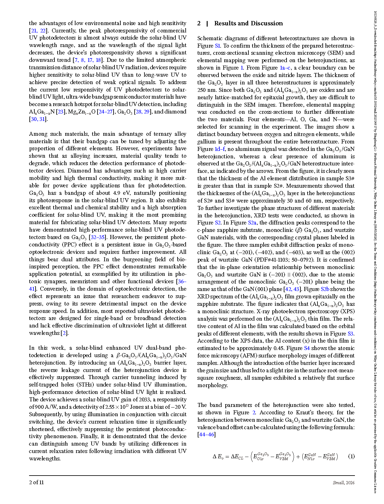
Fig. 2. (a) X-ray photoelectron spectra of different materials, (b) the optical UV–vis light transmittance of different materials, and (c) aschematic energy band diagram of the heterojunction.
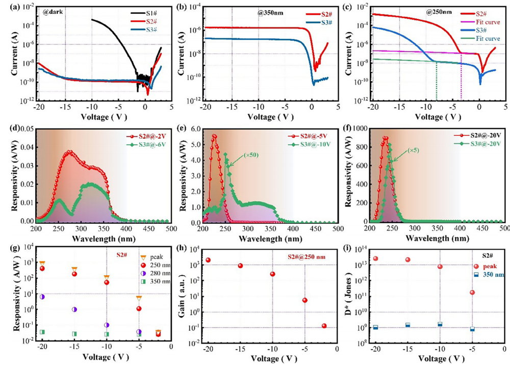
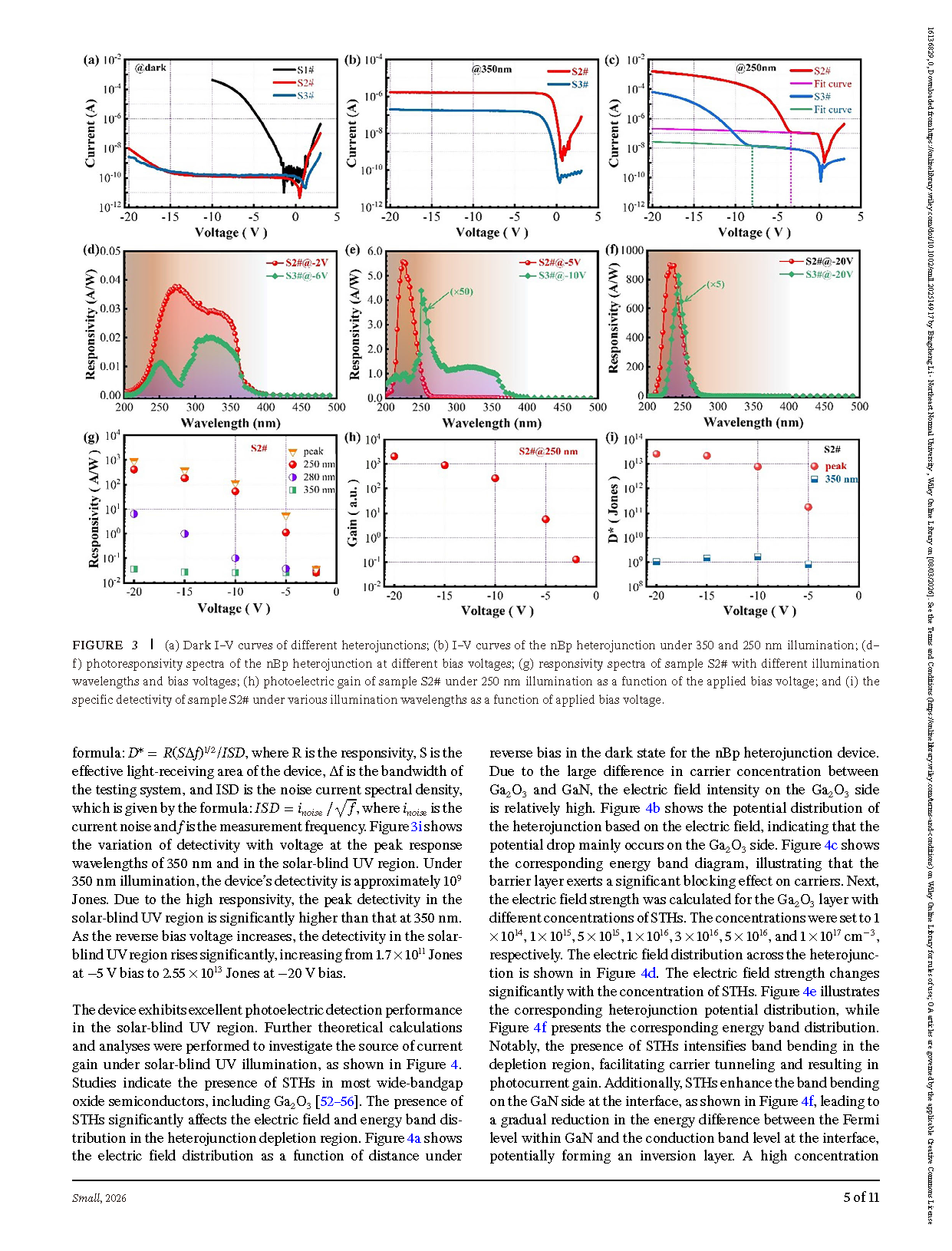
Fig. 3. (a) Dark I–V curves of different heterojunctions; (b) I–V curves of the nBp heterojunction under 350 and 250 nm illumination; (d–f) photoresponsivity spectra of the nBp heterojunction at different bias voltages; (g) responsivity spectra of sample S2# with different illumination wavelengths and bias voltages; (h) photoelectric gain of sample S2# under 250 nm illumination as a function of the applied bias voltage; and (i) the specific detectivity of sample S2# under various illumination wavelengths as a function of applied bias voltage.
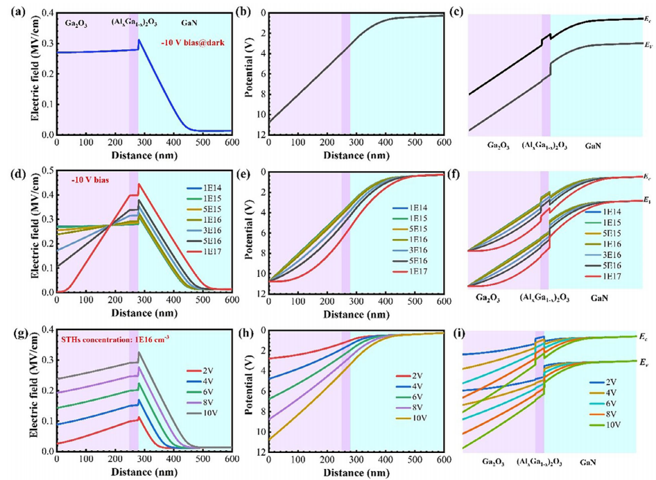
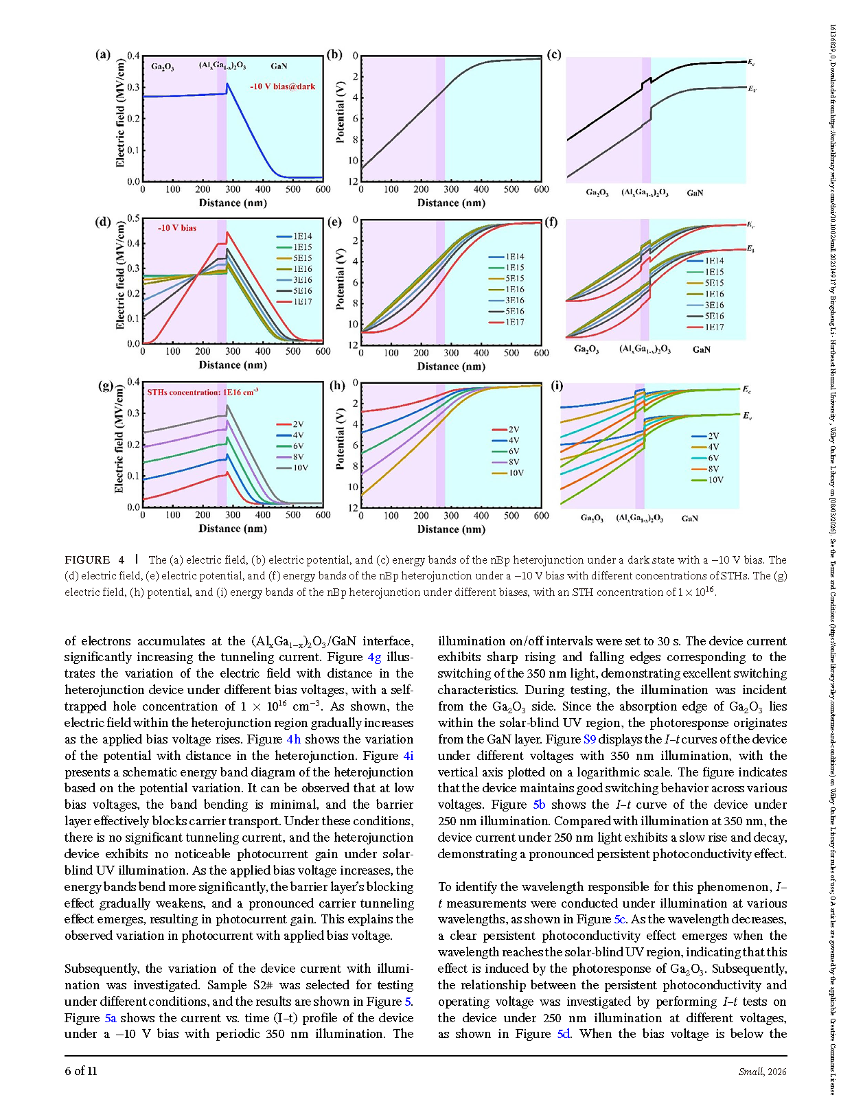
Fig. 4. The (a) electric field, (b) electric potential, and (c) energy bands of the nBp heterojunction under a dark state with a -10 V bias. The (d) electric field, (e) electric potential, and (f) energy bands of the nBp heterojunction under a -10 V bias with different concentrations of STHs. The (g) electric field, (h) potential, and (i) energy bands of the nBp heterojunction under different biases, with an STH concentration of 1 × 10¹⁶.
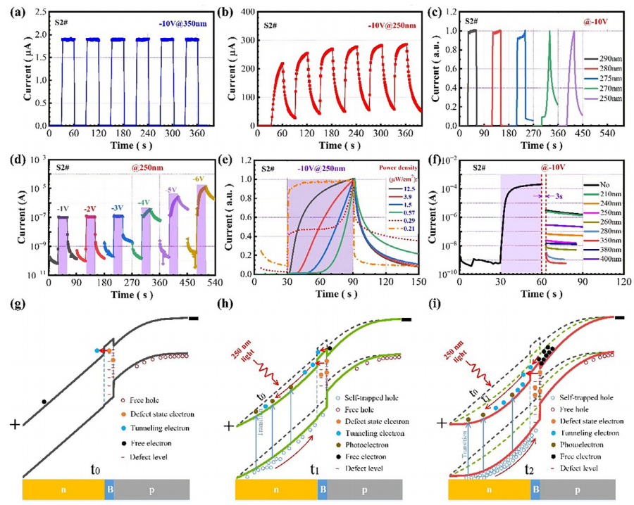
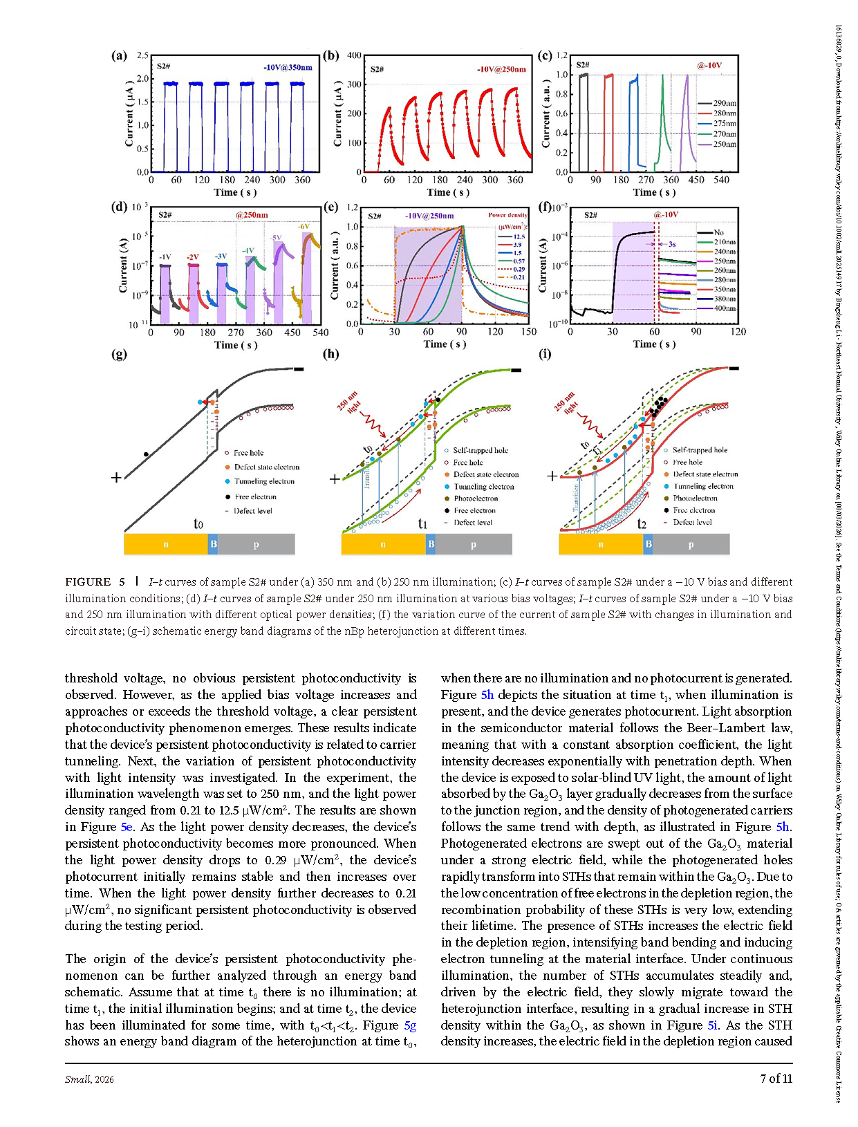
Fig. 5. I–t curves of sample S2# under (a) 350 nm and (b) 250 nm illumination; (c) I–t curves of sample S2# under a -10 V bias and different illumination conditions; (d) I–t curves of sample S2# under 250 nm illumination at various bias voltages; I–t curves of sample S2# under a -10 V bias and 250 nm illumination with different optical power densities; (f) the variation curve of the current of sample S2# with changes in illumination and circuit state; (g–i) schematic energy band diagrams of the nBp heterojunction at different times.
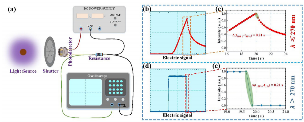
Fig. 6. (a) A schematic diagram of the photodetection circuit; I–t curves of the nBp heterojunction device under UV light with (b) λ ≤ 270 nm and (d) λ > 270 nm; (c–e) enlarged views of different I–t decay times.
DOI:
doi.org/10.1002/smll.202514917