Paper Sharing
【Member Papers】Origin of suppressed ferroelectricity in κ-Ga₂O₃: interplay between polarization and lattice domain walls
日期:2026-03-13阅读:304
Researchers from the Institute of Semiconductors, Chinese Academy of Sciences have published a dissertation titled "Origin of suppressed ferroelectricity in κ-Ga2O3: interplay between polarization and lattice domain walls" in npj Computational Materials.
Project Support
This work is supported by the National Key R&D Program of China (2022YFB3605400). Y.Z. is supported by the Postdoctoral Fellowship Program of CPSF (GZB20240720) and Project funded by China Postdoctoral Science Foundation (2024M763182). Z.W. is supported by the National Natural Science Foundation of China (12174380). R.L. acknowledges the National Natural Science Foundation of China (grant no. 22533001).
Background
Ferroelectric (FE) materials exhibit switchable, nonvolatile polarization, high breakdown fields, and low leakages. These attributes enable technologies from energy harvesting and sensors, to spintronics, and nonvolatile memory. Remanent polarization and coercive field are two fundamental parameters that govern the functional performance of these applications. They directly determine the energy consumption, readout margin, storage performance, and reliability in memory devices. Yet across bulk crystals, thick films, and two -dimensional (2D) systems, experiments often report remanent polarization and coercive field far below state -of-the -art predictions, even when depolarization fields are negligible. For instance in κ -Ga 2 O 3, (1) predicted remanent polarization by first -principles calculations (~23 μC/cm2, comparable to ZrHfO2) vastly exceeds experimental values (< 8.6 μC/cm2) ; (2) coercive fields obtained from fitting by the ab initio results to Landau -Ginzburg (L - G) theory (~3 MV/cm) are also an order of magnitude greater than measured values (< 0.5 MV/cm) . Another example is in 2D sliding ferroelectrics where the difference s are even more significant (e.g. 243 MV/cm predicted vs 3 MV/cm measured for bilayer h -BN). These large, systematic discrepancies pose a serious challenge to the reliability of standard theoretical approach, and call for more advanced methods to capture the missing physics.
Abstract
Remanent polarization and coercive field in ferroelectrics are often predicted to be high, yet experimentally observed to be much lower-an inconsistency that hinders the rational design of functional materials and devices. We identify a hidden mechanism underlying this discrepancy: the interaction between polarization domain walls (PDWs) and lattice domain walls (LDWs) that standard models omit. Using κ-Ga2O3 as a representative ferroelectric, we develop a machine-learning potential trained on ab initio molecular-dynamics data to capture realistic polarization switching. Our simulations reveal that PDWs become topologically blocked at 120° LDWs, stabilizing residual domain-wall networks that suppress remanent polarization while enabling rapid, low-field switching by bypassing slow nucleation. The blocking strengthens as lattice domains shrink, offering a new strategy for tuning ferroelectric performance through lattice-domain engineering. The mechanism not only reconciles theoretical with experimental results but also provides a practical approach for improving ferroelectric performance.
Conclusion
We report a nontrivial ferroelectric switching mechanism from the interplay between polarization domain walls (PDWs) and lattice domain walls (LDWs), and how it closes the gap between experimental observations and theoretical predictions in κ-Ga2O3. By combining density functional theory, a long-range machine learning force field, and large-scale molecular dynamics, we show that the out-of-plane polarization flips through an in -plane shear and sliding of Ga-O layers, establishing κ-Ga2O3 as a sliding -like ferroelectric. Our simulations capture both stages of field -driven switching: slow nucleation followed by rapid domain wall motion. Two types of PDW appear. The (100) wall travels twice as fast as the (010) wall, the latter of which has a velocity following Merz’s law at low fields. These data reconcile the experimentally low coercive field with the Kolmogorov-Avrami-Ishibashi model. Critically, the 120° LDWs that exist in real samples can topologically terminate PDW propagation. This pinning effect leaves a stable network of residual PDWs with LDWs. This network reduces the remanent polarization to a fraction of its intrinsic value, yet provides persistent nucleation seeds, and thus enables rapid, low -field switching after initiation. Our results demonstrate a generic mechanism for sliding ferroelectrics, enrich the domain engineering for fast, low power ferroelectric devices, and provide a transferable framework for the study of other ferroelectric systems.
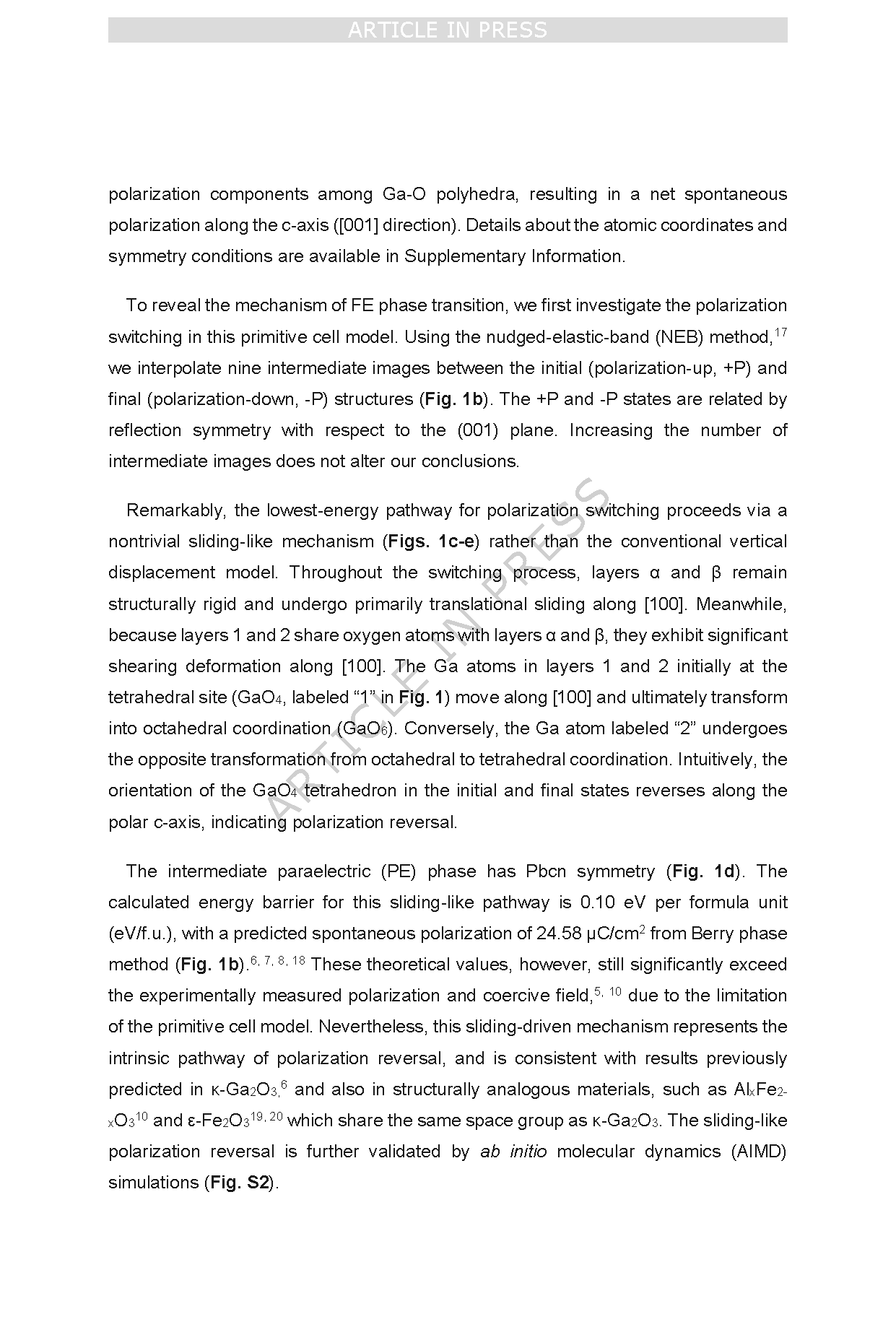
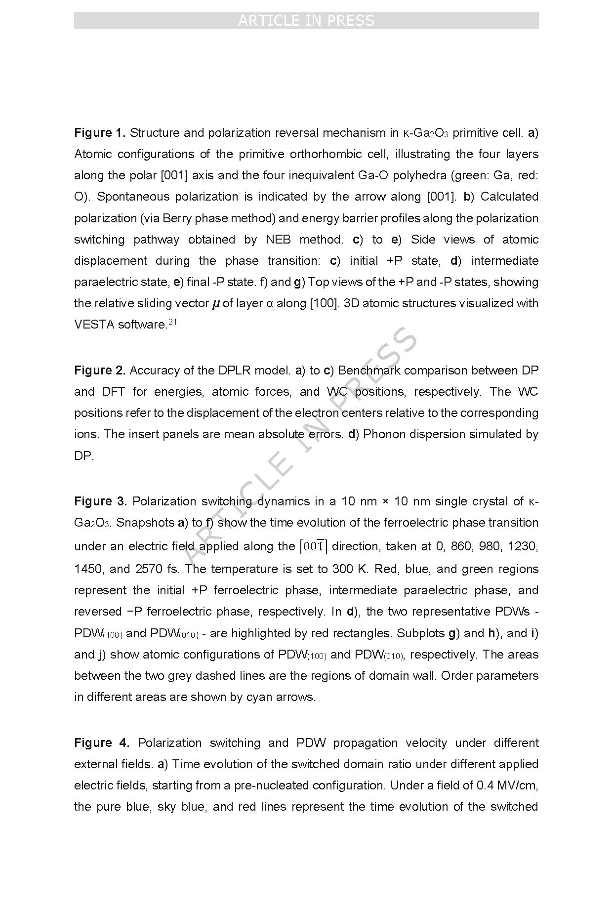
Figure 1. Structure and polarization reversal mechanism in κ-Ga2O3 primitive cell. a) Atomic configurations of the primitive orthorhombic cell, illustrating the four layers along the polar [001] axis and the four inequivalent Ga-O polyhedra (green: Ga, red: O). Spontaneous polarization is indicated by the arrow along [001]. b) Calculated polarization (via Berry phase method) and energy barrier profiles along the polarization switching pathway obtained by NEB method. c) to e) Side views of atomic displacement during the phase transition: c) initial +P state, d) intermediate paraelectric state, e) final -P state. f) and g) Top views of the +P and -P states, showing the relative sliding vector μ of layer α along [100]. 3D atomic structures visualized with VESTA software.
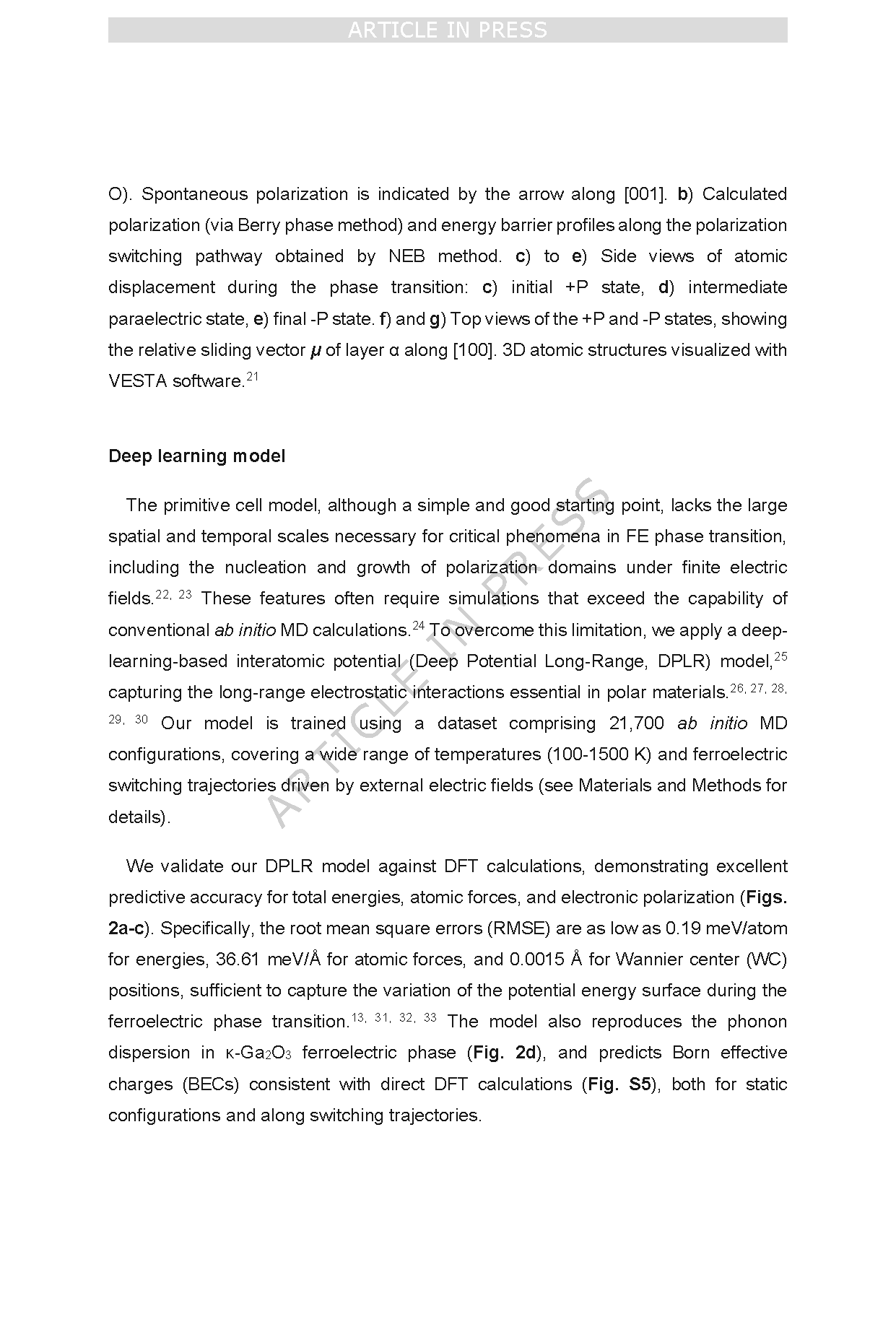
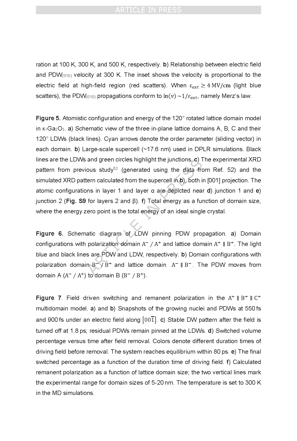
Figure 2. Accuracy of the DPLR model. a) to c) Benchmark comparison between DP and DFT for energies, atomic forces, and WC positions, respectively. The WC positions refer to the displacement of the electron centers relative to the corresponding ions. The insert panels are mean absolute errors. d) Phonon dispersion simulated by DP.
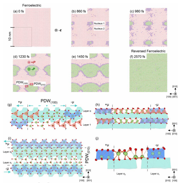
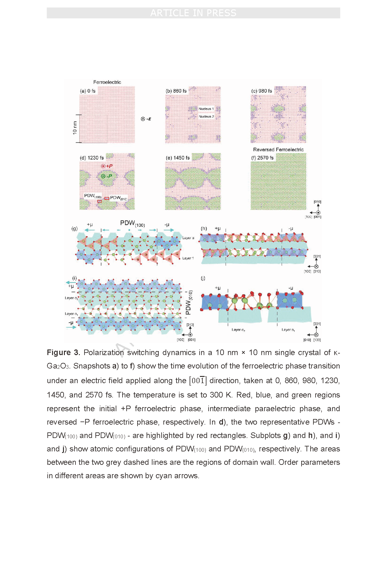
Figure 3. Polarization switching dynamics in a 10 nm × 10 nm single crystal of κ-Ga2O3. Snapshots a ) to f) show the time evolution of the ferroelectric phase transition under an electric field applied along the [00-1] direction, taken at 0, 860, 980, 1230, 1450, and 2570 fs. The temperature is set to 300 K. Red, blue, and green regions represent the initial +P ferroelectric phase, intermediate paraelectric phase, and reversed −P ferroelectric phase, respectively. In d), the two representative PDWs - PDW(100) and PDW(010) - are highlighted by red rectangles. Subplots g) and h) , and i) and j) show atomic configurations of PDW(100) and PDW(010), respectively. The areas between the two grey dashed lines are the regions of domain wall. Order parameters in different areas are shown by cyan arrows.
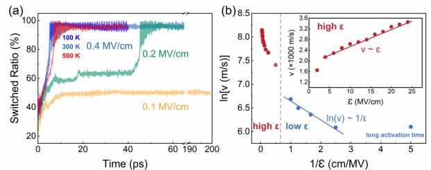
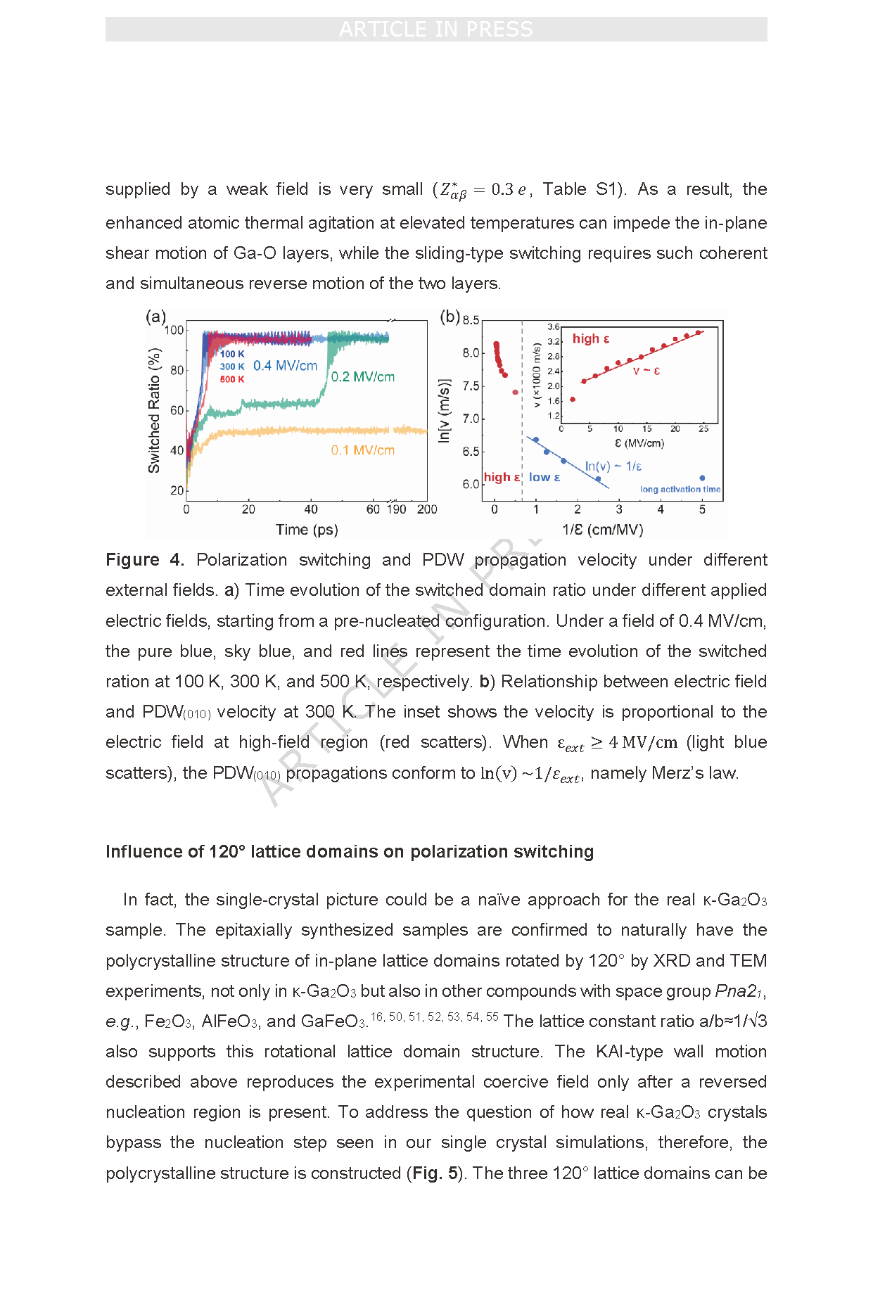
Figure 4. Polarization switching and PDW propagation velocity under different external fields. a) Time evolution of the switched domain ratio under different applied electric fields, starting from a pre -nucleated configuration. Under a field of 0.4 MV/cm, the pure blue, sky blue, and red lines represent the time evolution of the switched ration at 100 K, 300 K, and 500 K, respectively. b) Relationship between electric field and PDW(010) velocity at 300 K. The inset shows the velocity is proportional to the electric field at high -field region (red scatters). When εext ≥ 4 MV /cm (light blue scatters), the PDW(010) propagations conform to ln ( v ) ~ 1 /εext, namely Merz’s law.
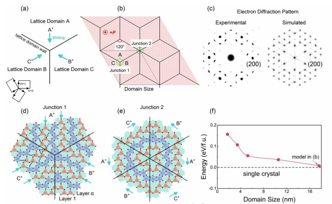
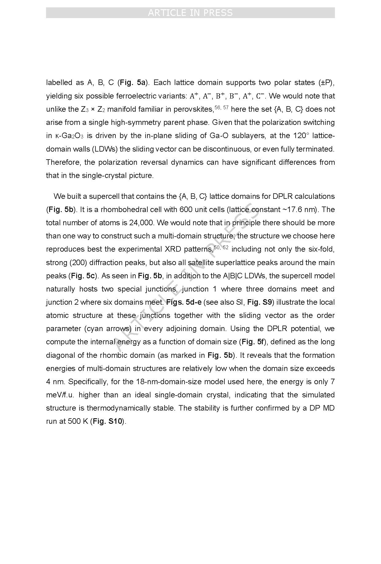
Figure 5 . Atomistic configuration and energy of the 120° rotated lattice domain model in κ -Ga2O3. a) Schematic view of the three in -plane lattice domains A, B, C and their 120° LDWs (black lines). Cyan arrows denote the order parameter (sliding vector) in each domain. b) Large -scale supercell (~17.6 nm) used in DPLR simulations. Black lines are the LDWs and green circles highlight the junctions. c) The experimental XRD pattern from previous study52 (generated using the data from Ref. 5 2) and the simulated XRD pattern calculated from the supercell in b), both in [001] projection. The atomic configurations in layer 1 and layer α are depicted near d) junction 1 and e) junction 2 ( Fig. S9 for layers 2 and β). f) Total energy as a function of domain size, where the energy zero point is the total energy of an ideal single crystal.
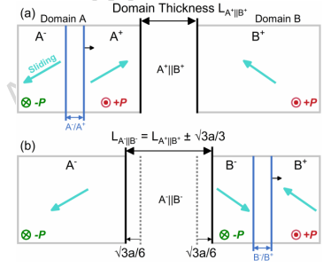
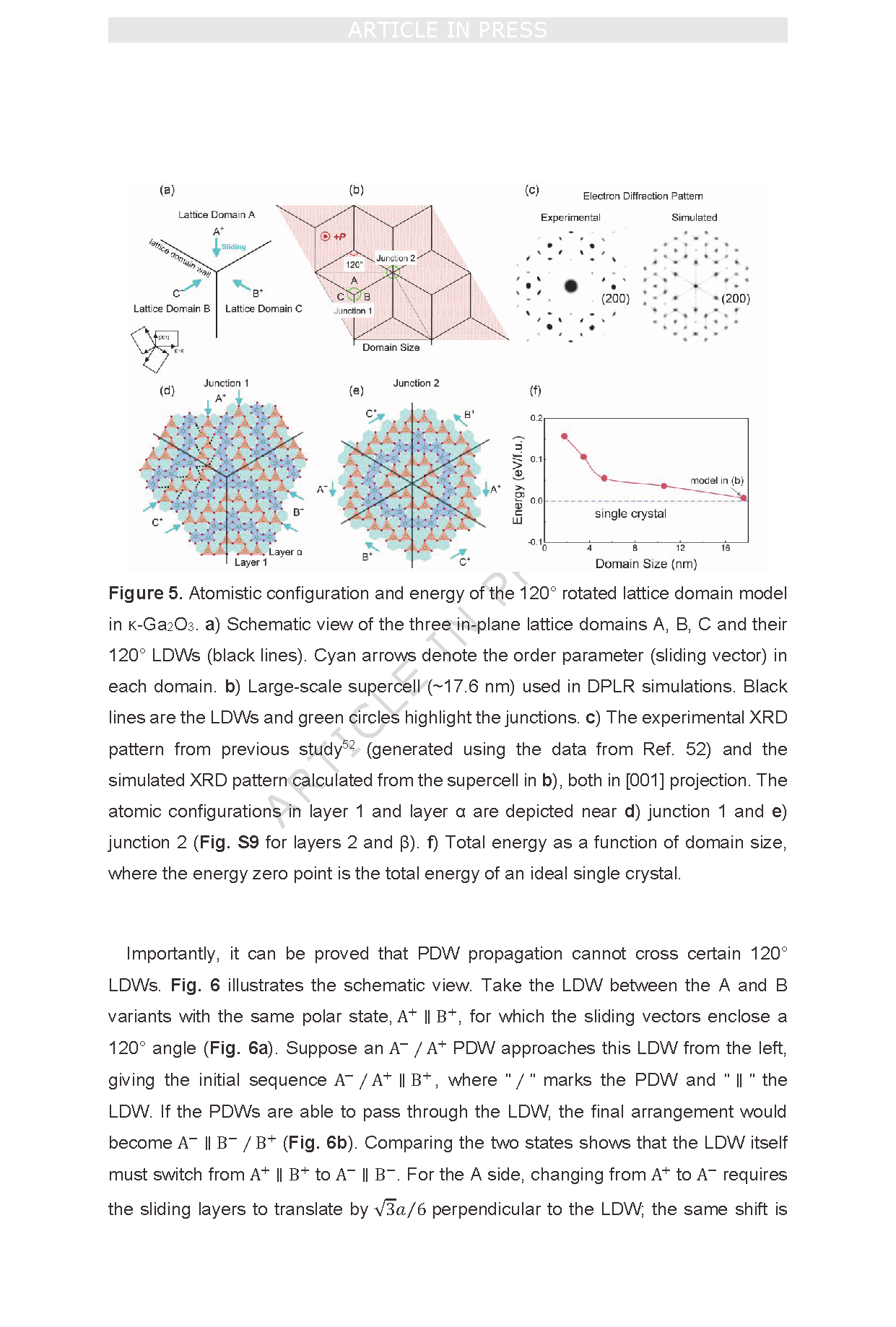
Figure 6. Schematic diagram of LDW pinning PDW propagation. a) Domain configurations with polarization domain A− ∕ A+ and lattice domain A + ∥ B +. The light blue and black lines are PDW and LDW, respectively. b) Domain configurations with polarization domain B− ∕ B+ and lattice domain A− ∥ B−. The PDW moves from domain A ( A− ∕ A+) to domain B ( B− ∕ B+).
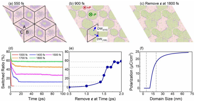
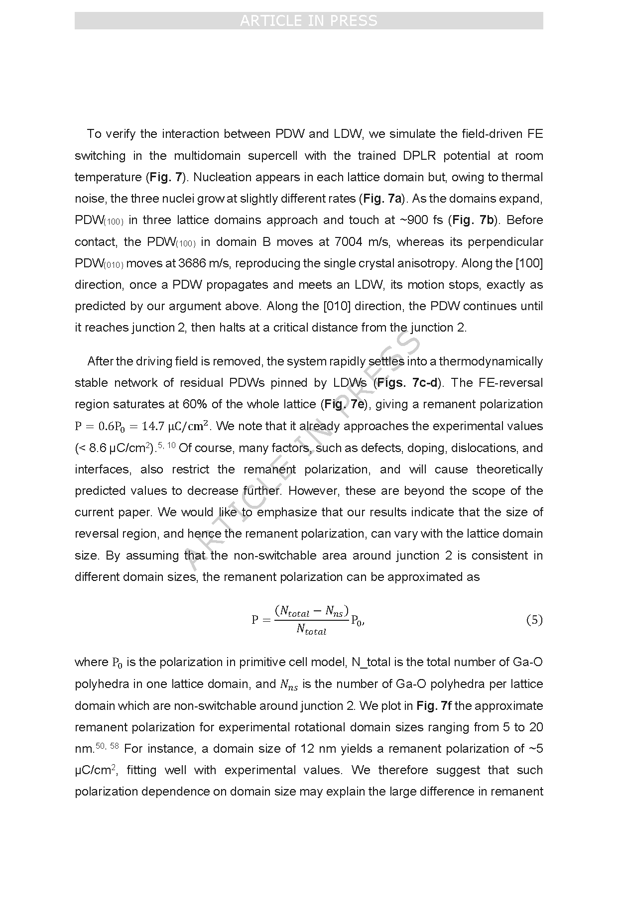
Figure 7. Field driven switching and remanent polarization in the A+ ∥ B+ ∥ C+ multidomain model. a ) and b) Snapshots of the growing nuclei and PDWs at 550 fs and 900 fs under an electric field along [00-1]. c) Stable DW pattern after the field is turned off at 1.8 ps; residual PDWs remain pinned at the LDWs. d) Switched volume percentage versus time after field removal. Colors denote different duration times of driving field before removal. The system reaches equilibrium within 80 ps. e) The final switched percentage as a function of the duration time of driving field. f) Calculated remanent polarization as a function of lattice domain size; the two vertical lines mark the experimental range for domain sizes of 5 -20 nm. The temperature is set to 300 K in the MD simulations.
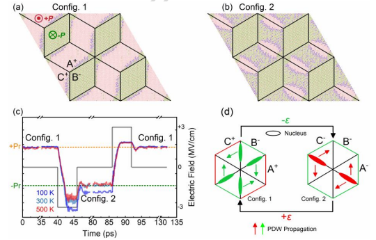
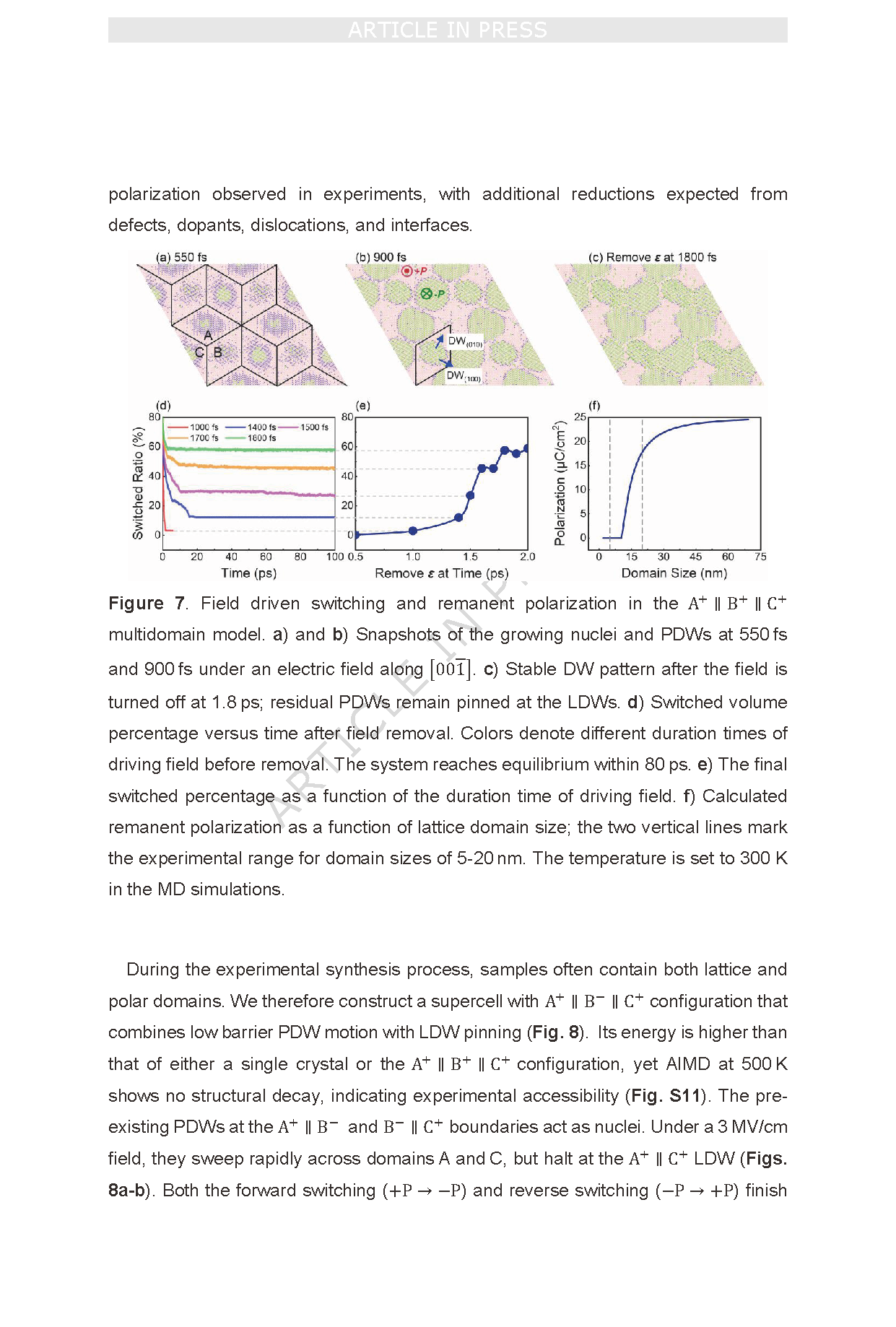
Figure 8. Field driven switching in the A+ ∥ B+ ∥ C+ multidomain model. a) Initial domain arrangement with positive remanent polarization (config. 1). b) Configuration after the driving field is applied (config. 2). These two polarization configurations are extracted from the MD trajectory at 300 K. c) Time evolution of remanent polarization under driving electric pulses (max intensity: 3 MV/cm). d) Schematic of forward ( + P → − P) and reverse ( − P → + P) switching. Red and green areas indicate +P and -P regions, respectively.
DOI:
doi.org/10.1038/s41524-026-02022-z