


News Trends
【Domestic News】Gallium Oxide Highlighted in China’s 15th Five-Year Plan: Fourth-Generation Semiconductors Enter a Critical Window
日期:2026-03-15阅读:1253
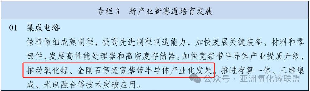
On March 13, the Outline of the 15th Five-Year Plan for National Economic and Social Development of the People's Republic of China was officially released. In the section outlining the development of frontier new materials, ultra-wide bandgap semiconductors such as Gallium Oxide and diamond were identified as key areas for future breakthroughs.
This statement indicates that Gallium Oxide has moved beyond being merely a long-standing academic research focus and has formally entered the core vision of China’s national strategic new-materials system.
From a material perspective, Gallium Oxide (Ga₂O₃) possesses an ultra-wide bandgap of approximately 4.8 eV and a theoretical breakdown electric field of about 8 MV/cm. In terms of the Baliga figure of merit for power devices, its performance significantly surpasses that of traditional power semiconductor materials such as silicon, silicon carbide, and gallium nitride. As a result, Gallium Oxide is widely regarded as a promising candidate material for next-generation high-voltage power devices.
At the same time, Gallium Oxide offers another major advantage: large-size single-crystal substrates can be grown using melt-growth methods. Compared with materials such as silicon carbide, this approach offers significant potential advantages in substrate manufacturing costs, which is considered an important factor driving its industrialization.
Breaking the Performance Ceiling of Traditional Materials
From a broader technological perspective, Gallium Oxide belongs to the fourth-generation semiconductor material system.
The fourth generation of semiconductors generally refers to ultra-wide bandgap materials represented by Gallium Oxide (Ga₂O₃), diamond, and aluminum nitride (AlN). The industry widely recognizes that these materials typically have bandgaps exceeding 4.5 eV, far larger than those of the previous three generations of semiconductors.
If silicon ushered in the information age, and silicon carbide and gallium nitride drove the efficiency revolution in power electronics, then fourth-generation semiconductors are more like aerospace-grade carbon-fiber composites—they directly break through the performance limits of traditional semiconductor materials.
Under extreme conditions such as ultra-high voltage, high temperature, strong radiation, and ultra-high frequency, these materials can still operate reliably. Therefore, they are considered key enabling materials for cutting-edge fields including 6G communications, ultra-high-voltage power grids, aerospace, and deep-space exploration.
It should be noted that fourth-generation semiconductors are not a simple replacement for previous generations, but rather an expansion of the application boundaries of semiconductor technology.
At present, the overall field of fourth-generation semiconductors remains in the transitional stage from laboratory breakthroughs to pilot-scale production. The industrialization progress of different materials varies significantly, while major technology powers around the world are accelerating their strategic deployments in this area.
Gallium Oxide: The Fastest-Advancing Material Toward Commercialization
Among the three core materials, Gallium Oxide is widely regarded as the closest to large-scale commercial application.
A key reason is that Gallium Oxide substrates can be grown using melt-growth techniques, which theoretically enable significantly lower substrate costs. Some studies suggest that its potential cost could be as low as one-tenth that of silicon carbide, while also offering a certain level of compatibility with existing silicon-based production lines. As a result, its industrialization barrier is relatively low.
Globally, Japanese companies have long been at the forefront of Gallium Oxide industrialization. For example, Novel Crystal Technology (NCT) in Japan has already begun delivering 6-inch Gallium Oxide wafer samples, and plans to provide epitaxial wafer samples in 2027, with mass production targeted for 2029.
Meanwhile, China has achieved a series of breakthroughs in the Gallium Oxide field in recent years.
Between 2025 and 2026, the domestic industry witnessed a wave of major advances. For instance:
● Hangzhou Gallium Semiconductor released the world’s first 8-inch Gallium Oxide single-crystal substrate, while its 6-inch substrates have already achieved batch shipments. In early 2026, the company also successfully achieved 8-inch homoepitaxy on Gallium Oxide substrates.
● The Shanghai Institute of Optics and Fine Mechanics of the Chinese Academy of Sciences, together with Hangzhou Fujia Gallium, successfully produced 8-inch Gallium Oxide crystals using the Vertical Bridgman (VB) method for the first time internationally, significantly reducing production costs.
These developments indicate that China is gradually establishing competitive technological routes in Gallium Oxide single-crystal growth.
A Key Material Under National Strategic Demand
From the perspective of national strategic demand, Gallium Oxide sits precisely at the intersection of three core development priorities emphasized in the Plan.
First, it represents an important direction for addressing key material bottlenecks.
Within the semiconductor materials system, silicon, silicon carbide, and gallium nitride have already formed relatively mature industrial ecosystems. Gallium Oxide, as an emerging ultra-wide bandgap semiconductor material, is currently at the center of a global industrialization race. Breakthroughs in crystal growth, epitaxial materials, power devices, and related equipment could provide China with an important opportunity to achieve technological leaps in next-generation power semiconductors.
Second, it serves as a foundational material for the development of new productive forces.
Future energy systems, electric vehicles, rail transit, power grids, and aerospace applications all demand power devices with higher efficiency, higher voltage tolerance, and lower losses. Gallium Oxide power devices are expected to play a key role in high-voltage power conversion, power electronic systems, and electronics for extreme environments.
Third, it represents a strategic high ground in frontier material competition.
Unlike many traditional materials, the Gallium Oxide industry remains at a stage where global technological pathways and industrial structures have not yet been fully established. Significant room for innovation still exists in areas such as single-crystal growth, epitaxial technology, device structures, and application scenarios.
With continued policy support and sustained industrial investment, there remains a real possibility for technological “leadership” in this emerging material field.
The Next Five Years: A Critical Phase for Gallium Oxide Industrialization
From an industrial-chain perspective, the development of Gallium Oxide is expected to drive coordinated upgrades across multiple segments, including crystal growth, epitaxial materials, power devices, and related equipment, gradually forming a new semiconductor materials ecosystem.
As demand continues to expand in areas such as new energy vehicles, renewable energy systems, grid upgrades, and deep-space exploration, Gallium Oxide is likely to become one of the key strategic materials of the ultra-wide bandgap semiconductor era.
In the development blueprint outlined by the 15th Five-Year Plan, Gallium Oxide stands at the intersection of technological breakthroughs, industrial upgrading, and national strategic demand.
Over the next five years, with sustained progress in fundamental research and accelerating industrialization, Gallium Oxide materials and device technologies are expected to move from the laboratory toward large-scale commercial applications.
