


Member News
【Member News】GAREN SEMI Successfully Achieves 8-inch Gallium Oxide Homoepitaxy
日期:2026-03-15阅读:564
In March 2026, Hangzhou Garen Semiconductor Co., Ltd. (hereinafter referred to as "GAREN SEMI") made a major technological breakthrough in epitaxy technology, successfully realizing high-quality 8-inch gallium oxide homoepitaxial growth for the first time worldwide. The test results of the epitaxial wafer show that: the epitaxial film thickness is > 10 μm with a thickness variance σ < 1%; the average carrier concentration of the epitaxial layer is 1.79×10¹⁶ cm⁻³.
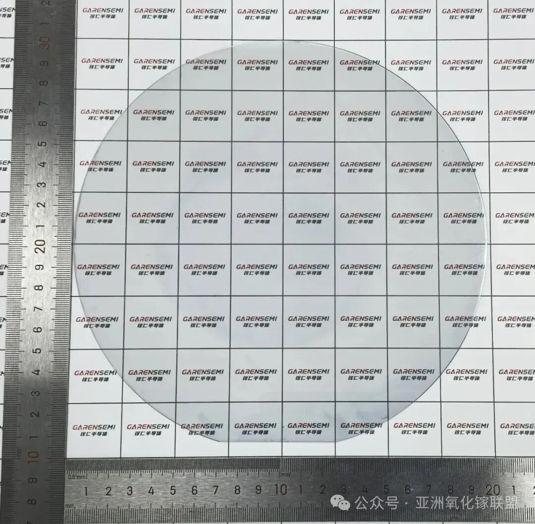
Fig.1 GAREN SEMI 8-inch Gallium Oxide Homoepitaxial Wafer
Excellent Performance
Film thickness testing shows that the 8-inch gallium oxide epitaxial wafer has an average thickness of 13.05 μm with excellent thickness uniformity and a variation of merely σ=0.58%. This data fully attests to the superior controllability and consistency of GAREN SEMI's epitaxial growth process. For power electronic devices, high voltage withstand capability is a core performance attribute, and the epitaxial layer typically serves as the drift region—the primary area responsible for the device's voltage blocking capability. Notably, the thickness of the drift region is positively correlated with the device's breakdown voltage, making a thick, highly uniform epitaxial layer a fundamental guarantee for manufacturing high-performance high-voltage power devices.
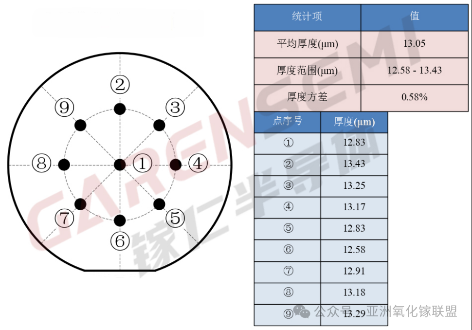
Fig.2 GAREN SEMI 8-inch epitaxial film thickness test point distribution and corresponding results
Tested via the capacitance-voltage (C-V) measurement method, the carrier concentration of the epitaxial layer ranges from 1.30×10¹⁶ cm⁻³ to 2.06×10¹⁶ cm⁻³, with an average carrier concentration of 1.79×10¹⁶ cm⁻³ and a standard deviation of 12.54%. Such superior electrical properties render the 8-inch epitaxial wafer well-suited for the fabrication of high-voltage power devices, providing high-quality material support for the subsequent R&D and mass production of related devices.
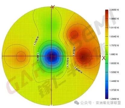
Fig.3 C-V Test Results of GAREN SEMI 8-inch Epitaxial Wafer
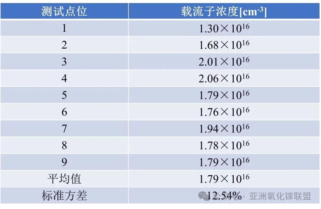
Fig.4 Carrier Concentration Distribution Cloud Map of GAREN SEMI 8-inch Epitaxial Wafer
Reshape The Industrial Pattern
In response to the key deployment requirements of the national 15th Five-Year Plan for promoting ultra-wide bandgap semiconductor materials such as gallium oxide and diamond, and driven by the rapid development of strategic emerging industries including new energy, photovoltaic power generation, radar detection, and 5G mobile communications, gallium oxide—an ultra-wide bandgap semiconductor material with higher bandgap width and breakdown electric field strength—has become an important direction for China’s scientific and technological self-reliance, independent control of the industrial chain, and cultivation of new quality productive forces. It has received high attention and systematic layout from the industrial, scientific research, and policy sectors.
Figure 5 Key Deployment of Gallium Oxide Materials in the Outline of the 15th Five-Year Plan for National Economic and Social Development of the People's Republic of China
The Characteristics and Application Prospects of Gallium Oxide
Gallium oxide single crystals boast a portfolio of outstanding physical properties:
Fig.6 Physical Parameters of Gallium Oxide Single Crystal and Benchmark Diagram of Gallium Oxide Power Transistors
(Ref: S. J. Pearton, et al., Appl. Phys. Rev., 5, 2018, 011301;A. J. Green, et al., APL Mater., 10, 2022, 029201)
Based on its excellent physical properties, gallium oxide can support the application of high-reliability devices under extreme high voltage (device voltage resistance above 2000V), extreme power (100kW level), extreme working conditions (high radiation, wide temperature range, high humidity, long service life) and extreme environments (deep space, deep sea, deep earth, strong electromagnetic interference). Therefore, it has broad application prospects in fields such as new energy vehicles, photovoltaic energy storage, smart grids, rail transit, commercial aerospace, and 5G communication, and has great market potential.
The Important Significance of 8-inch Gallium Oxide Homoepitaxial Growth
For a long time, the difficulty in preparing large-size, high-quality epitaxial wafers has been the core bottleneck restricting the industrialization of gallium oxide. Previously, the global mainstream technology was still at the 2-4 inch level, and the homoepitaxy technology was immature, which seriously limited device cost control and large-scale application.
The breakthrough of GAREN SEMI's 8-inch gallium oxide homoepitaxial wafer will completely change the development trajectory of the gallium oxide industry from three dimensions:
01 Break the Size Bottleneck
The size of the epitaxial wafer directly determines the number of devices that can be manufactured per wafer, which is the core prerequisite for large-scale production. Compared with the current mainstream 2-4 inch epitaxial wafers, the 8-inch gallium oxide homoepitaxial wafer of GAREN SEMI can produce a larger number of power devices per wafer, which can significantly reduce the unit cost of substrate, processing, packaging and other links.
02 Solve Quality Pain Points
Homoepitaxy is the optimal path for preparing high-performance gallium oxide devices — the epitaxial layer and the substrate have perfect lattice matching, which can effectively reduce lattice mismatch and defect density, and significantly improve key performance indicators of devices such as breakdown voltage, on-resistance, and switching speed. The 8-inch homoepitaxial wafer of GAREN SEMI has excellent crystal quality and low defect density, making it possible for gallium oxide to be applied in ultra-high voltage and high-power scenarios.
03 Accelerate Industrial Upgrading
The full realization of gallium oxide's performance advantages hinges critically on the capability to produce large-size, high-quality materials. GAREN SEMI's breakthrough in 8-inch homogeneous gallium oxide epitaxial wafers not only enhances China's global competitiveness in the fourth-generation semiconductor field but will also accelerate technological iterations in the global gallium oxide industry, ushering in a new "fourth-generation" era for the global semiconductor industry.
Consolidate Global Leadership
In March 2025, Garen Semiconductor successfully prepared the world's first 8-inch gallium oxide single crystal using independently developed casting method and processed the corresponding size single crystal substrate, demonstrating its technical capability in breaking through material size limits. This achievement marks that Garen Semiconductor has become the first enterprise in the world to master the 8-inch gallium oxide single crystal growth technology, setting a new global record for the size of gallium oxide single crystal.
Subsequently, Garen Semiconductor completed the 8-inch gallium oxide single crystal growth by Vertical Bridgman (VB) method in just one year, becoming the world's first leading manufacturer to realize the preparation of 8-inch gallium oxide single crystals with multiple technical routes and multiple crystal planes.
The growth of 8-inch gallium oxide homoepitaxial wafers not only solves the core bottleneck of gallium oxide industrialization, but also reshapes the competitive pattern of the global gallium oxide industry. Looking to the future, Garen Semiconductor will deepen industry-university-research cooperation with universities and research institutions, attract high-end technical talents, continuously promote technological iteration, consolidate its global leading position, strive to become a global leader in gallium oxide materials and equipment solutions, and contribute core strength to the high-quality development of China's semiconductor industry.
About GAREN SEMI
Hangzhou Garen Semiconductor Co., Ltd. is a world-leading provider of gallium oxide materials and equipment solutions, focusing on R&D and industrialization in the ultra-wide bandgap semiconductor field. The company’s core products include 2–8-inch gallium oxide single crystals and substrates (with 8-inch being the world’s first), gallium oxide Vertical Bridgman (VB) crystal growth equipment, gallium oxide epitaxial wafers, etc. It is committed to building a full-chain product system of “equipment–crystal–substrate–epitaxy” to provide systematic solutions for global customers. The company’s achievements in gallium oxide have been specially reported by well-known media including People’s Daily, Xinhua News Agency, Science and Technology Daily, Sina Finance, China Blue News, and The Paper.
Enterprise Honors Summary:
Recognized as a National-level Science and Technology Small and Medium-sized Enterprise and Zhejiang Innovative Small and Medium-sized Enterprise in 2023;Awarded Zhejiang Specialized, Sophisticated, Unique and New Small and Medium-sized Enterprise in 2024;Approved as a High-tech Enterprise in 2025;Won the SEMI Outstanding Contribution Award for Sustainable Development at SEMICON CHINA 2025, the Together Progress Award at the Jufeng Summit Forum (JFSC) and Compound Semiconductor Industry Expo, the Innovation Vitality Award of Zhejiang Semiconductor Industry, the Second Prize in the Enterprise Group of the 10th “Maker China” Zhejiang Provincial Finals, the Top 500 Enterprise Group of the 10th “Maker China” SME Innovation and Entrepreneurship Competition, and the 2024–2025 Semiconductor Material Industry Contribution Award;The major breakthrough in the preparation of 8-inch gallium oxide single crystals and substrates was selected as one of the “Top 10 Advances in China’s Third-Generation Semiconductor Technology 2025” and “Major Scientific and Technological Achievements 2025” by the Department of Science and Technology of Zhejiang Province;Led the formulation of 2 group standard drafts, participated in drafting 1 national standard, and participated in promoting 1 group standard draft in the gallium oxide field;Supported by the “5213” Excellence Program of Xiaoshan District, Hangzhou, Zhejiang Province, and approved to establish Zhejiang Enterprise Research Institute;Obtained the quality management system certification;Granted 14 authorized invention patents at home and abroad (including patents in the US, Japan and other countries), with more than 50 patents pending.
For more information about Garen Semiconductor and its products, please visit our official website: http://garen.cc/
Or contact us via the following ways:
Mr. Jiang: 15918719807
E-mail: jiangjiwei@garen.cc
Mr. Xia: 19011278792
E-mail: xianing@garen.cc
