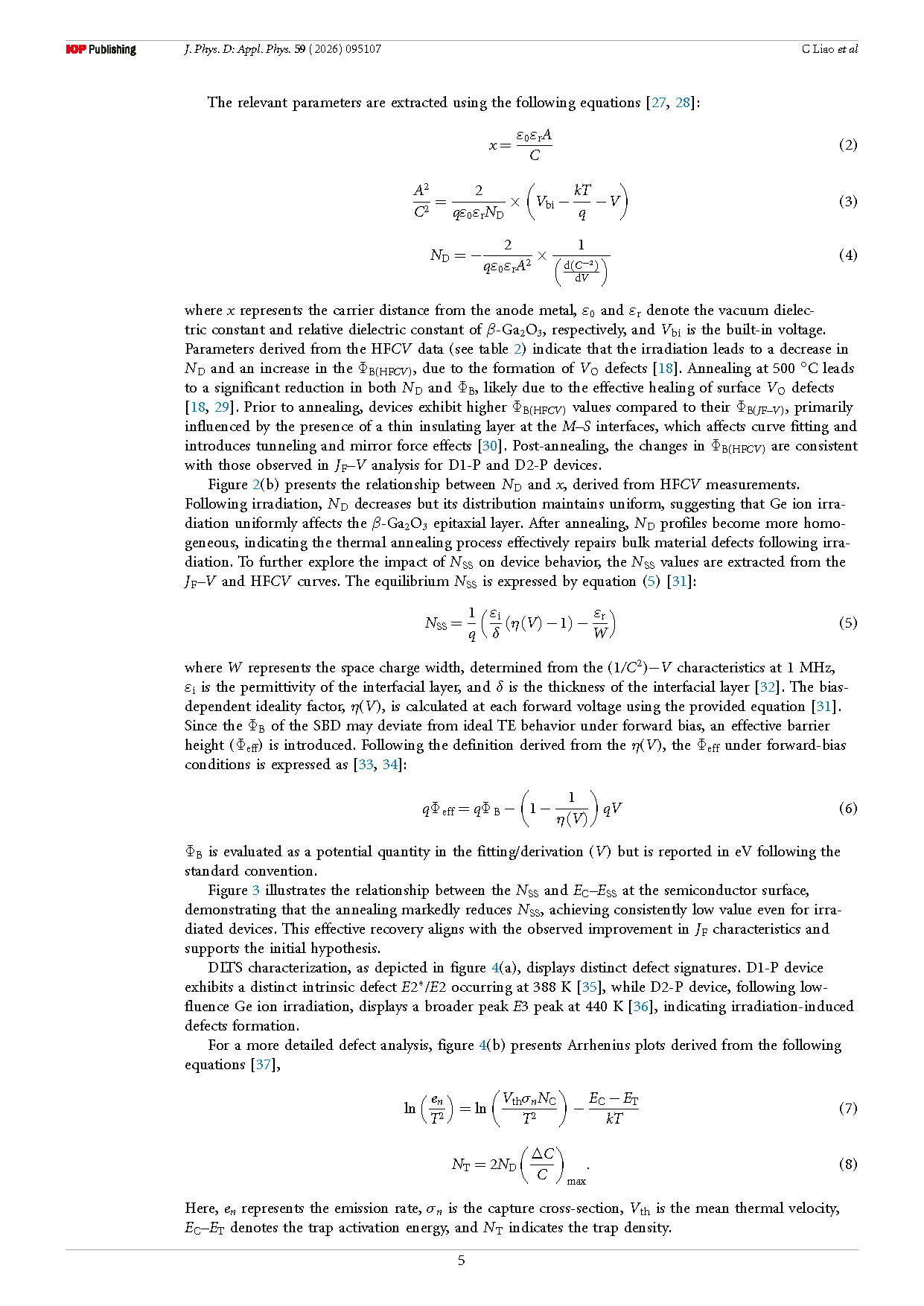
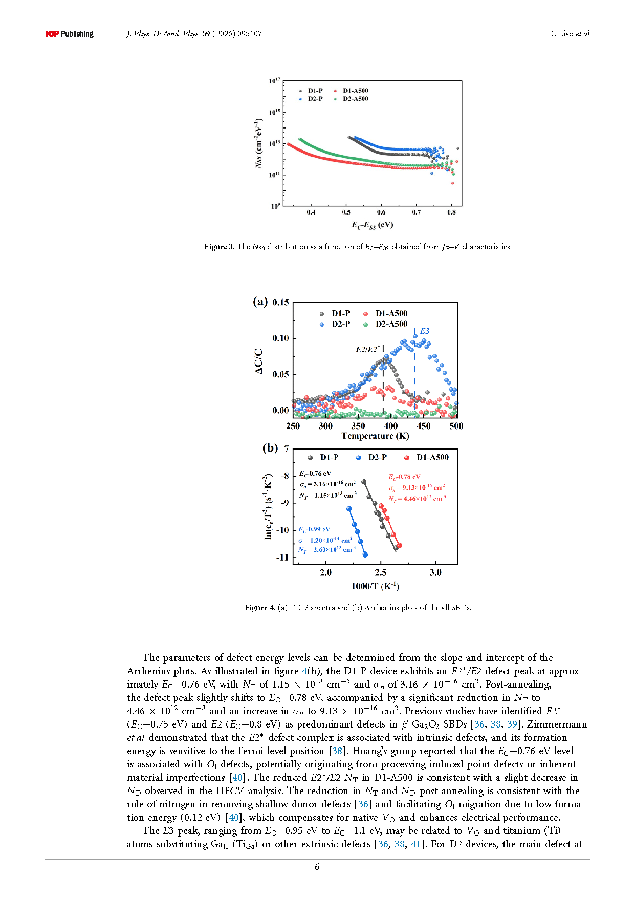
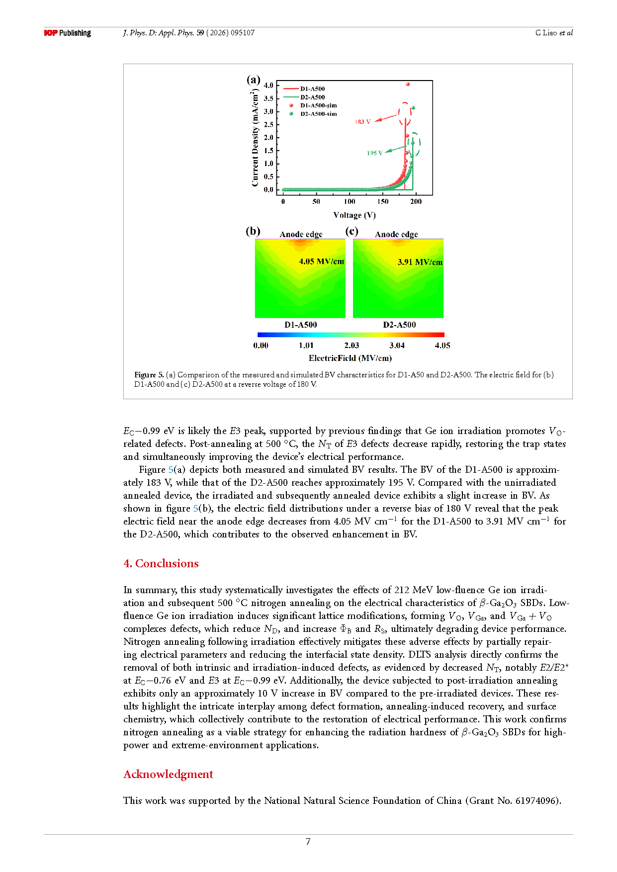
Background
Ultra-wide-bandgap semiconductor materials exhibit broad application prospects in aerospace electronics and high-power devices due to their high breakdown electric field, excellent thermal stability, and outstanding radiation resistance. Among them, β-Ga₂O₃ has a wide bandgap of approximately 4.8 eV and a theoretical breakdown field of up to 8 MV/cm. Its overall performance is significantly superior to that of third-generation semiconductor materials such as SiC and GaN. In particular, β-Ga₂O₃ is well suited for high-voltage rectifier devices such as Schottky barrier diodes (SBDs), offering advantages including low conduction loss and high breakdown voltage.
However, in space radiation environments, irradiation by high-energy particles can introduce deep-level defects in β-Ga₂O₃, such as oxygen vacancies and gallium vacancies, which damage the crystal structure and consequently affect the electrical performance of devices. Although post-irradiation annealing has been shown to partially repair defects and restore material properties, studies on the evolution mechanisms of defects under low-fluence heavy-ion irradiation and the repair effects of nitrogen annealing remain limited. Therefore, an in-depth investigation of the evolution behavior of irradiation-induced defects and their annealing recovery mechanisms is of great significance for improving the reliability of β-Ga₂O₃ devices operating in extreme aerospace environments.
Main Content
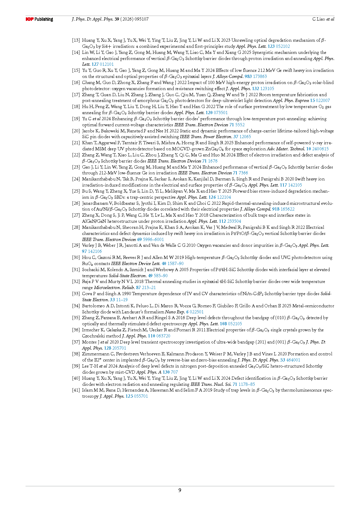
The ultra-wide-bandgap semiconductor β-Ga₂O₃ shows significant potential for applications in radiation-tolerant power electronic devices. This study systematically investigates the effects of low-fluence Ge ion irradiation and subsequent 500 °C nitrogen annealing on Au/Ni/β-Ga₂O₃ Schottky barrier diodes (SBDs). Electrical characterization results indicate that ion irradiation leads to device degradation, manifested as increases in the ideality factor (η), Schottky barrier height (ΦB), and series resistance (RS). However, nitrogen annealing at 500 °C effectively alleviates these degradations, mainly due to the recovery of irradiation-induced defects.
Deep Level Transient Spectroscopy (DLTS) analysis shows that before irradiation, an intrinsic defect level E₂/E₂* exists at EC − 0.76 eV. After irradiation, a new defect level E₃ appears at EC − 0.99 eV. Nitrogen annealing significantly reduces the concentrations of both E₂/E₂* and E₃ defects. Combined with Sentaurus TCAD simulations, the results reveal that the breakdown voltage (BV) of the device after annealing changes only slightly compared with that before irradiation.
This study elucidates the formation and recovery mechanisms of irradiation-induced defects in β-Ga₂O₃, confirming that nitrogen annealing is an effective approach to improving radiation resistance. The findings provide important references for the application of β-Ga₂O₃ devices in extreme environments.
Innovations
• The physical mechanism of defect generation induced by low-fluence Ge heavy-ion irradiation in β-Ga₂O₃ SBDs is revealed. The irradiation primarily introduces oxygen vacancies (VO), gallium vacancies (VGa), and their complex defects, and generates a new deep-level defect (E₃) at EC − 0.99 eV, which is identified as the fundamental cause of the degradation in device electrical performance.
• It is demonstrated that 500 °C nitrogen annealing has a significant recovery effect on irradiation-induced defects. This process effectively reduces the concentrations of E₂/E₂* and E₃ deep-level defects, as well as the interface state density, leading to a noticeable recovery of the degraded electrical parameters.
• A “low-fluence irradiation–nitrogen annealing” synergistic regulation strategy is proposed. This approach enables the recovery of device performance and provides a new strategy for optimizing the radiation resistance of β-Ga₂O₃ devices.
Conclusion
This work systematically investigates the effects of 212 MeV high-energy, low-fluence Ge ion irradiation and subsequent 500 °C nitrogen annealing on the electrical performance of β-Ga₂O₃ Schottky barrier diodes (SBDs). The results show that ion irradiation introduces VO, VGa, and VGa+VO complex defects in the device, resulting in a decrease in donor concentration (ND) and increases in the Schottky barrier height (ΦB) and series resistance (RS), which ultimately lead to device performance degradation.
The 500 °C nitrogen annealing process effectively repairs irradiation-induced damage. By reducing both the interface state density and the concentration of deep-level defects, the electrical parameters of the device are significantly restored. DLTS analysis further confirms that the concentrations of E₂/E₂* and E₃ defects decrease markedly after annealing.
This study reveals the mechanism of performance recovery through the combined effects of defect evolution, annealing repair, and interface regulation, confirming that nitrogen annealing is an effective method for improving the radiation tolerance of β-Ga₂O₃ SBDs. The findings provide an important reference for their application in extreme environments.
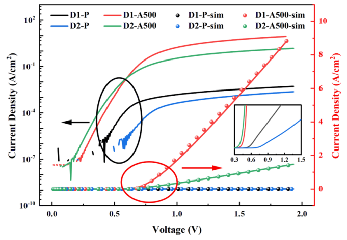
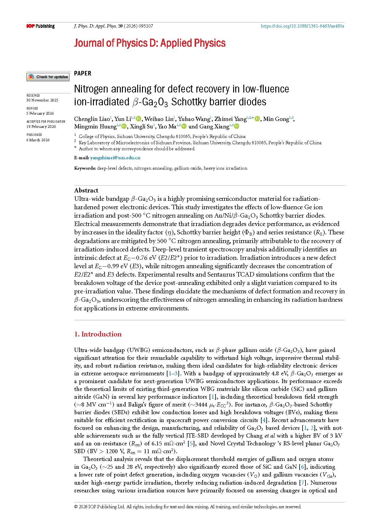
Figure 1. Experimental and simulated J–V characteristics plotted on linear and semi-logarithmic scales; the inset shows a magnified view of the J–V curve in the 0.3–1.5 V range.
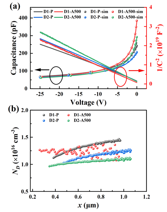
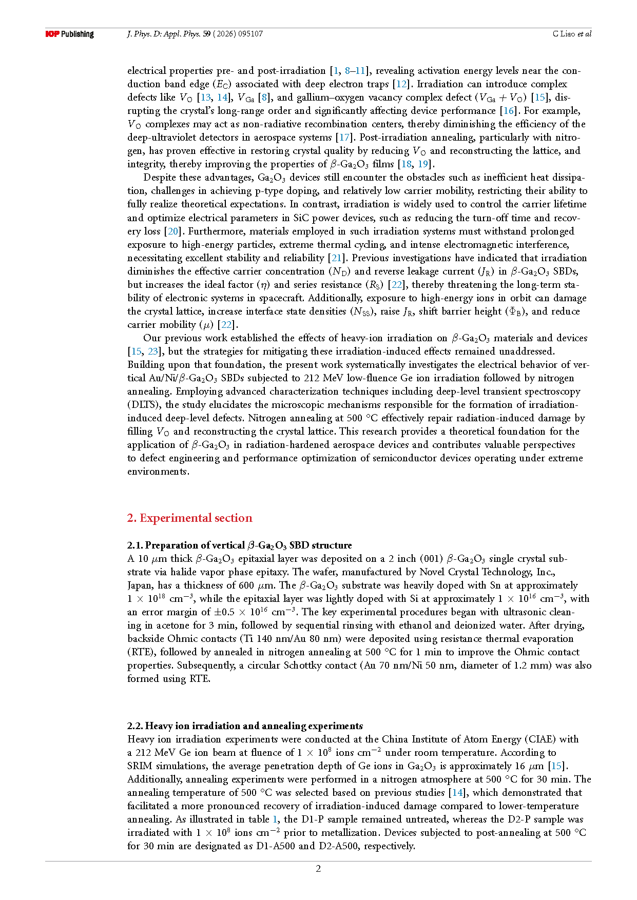
Figure 2. (a) Experimental and simulated HFCV (1/C²–V) characteristic curves; (b) ND–x relationship.
Figure 3. (a) DLTS spectra; (b) corresponding Arrhenius plot.
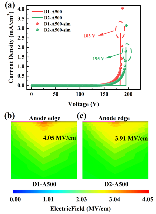
Figure 4. (a) Comparison of measured and simulated breakdown voltage characteristics of D1-A50 and D2-A500 devices; (b) electric field distribution of D1-A500 at a reverse voltage of 180 V; (c) electric field distribution of D2-A500 at a reverse voltage of 180 V.