Paper Sharing
【Member Papers】Epitaxial Growth of p-Type β-Ga₂O₃ Thin Films and Demonstration of a p–n Diode
日期:2026-03-19阅读:279
Researchers from the Hong Kong University of Science and Technology have published a dissertation titled " Epitaxial Growth of p-Type β-Ga2O3 Thin Films and Demonstration of a p–n Diode " in Advanced Electronic Materials.
Background
β-Ga2O3 has emerged as a prominent candidate for next-generation semiconductor materials, particularly in power electronics applications. Its appeal arises from two key attributes: an ultrawide bandgap (∼4.9 eV) and the relative ease of achieving n-type doping . These characteristics distinguish β-Ga2O3 from other wide-bandgap semiconductors such as aluminum nitride (AlN) and diamond . Recent advancements in melt-grown synthesis techniques have enabled the fabrication of bulk β-Ga2O3 crystals with diameters ranging from 6 to 8 inches, positioning this material as a cost-effective option for scalable production. Nonetheless, the absence of stable p-type conductivity remains a critical challenge for its full technological implementation. This limitation stems from difficult to introduce common acceptor elements with ionization energies of less than 1 eV, which inherently restricts the formation of effective p-type conductivity.
Conclusion
In summary, p-type conductivity in β-Ga2O3 was realized by employing Te-Mg co-doping via MOCVD, aiming to address a persistent challenge in this ultrawide-bandgap semiconductor. Thin films fabricated with this strategy exhibited tunable hole conduction, with measured room-temperature carrier concentrations ranging from 5.72 × 10¹⁴ to 1.78 × 1017 cm−3 and corresponding resistivities between 2064 and 32.4 Ω·cm. A mobility value of 5.29 cm2/V·s was measured under low-carrier-concentration conditions. Seebeck measurement confirms a p-type semiconductor with a positive Seebeck coefficient. A basic PN diode fabricated using this co-doped p-type film successfully demonstrates rectifying ability. Complementary DFT modelling and band analysis provide a potential mechanism that is proposed to both lower the Mg acceptor ionization barrier and elevate the valence band maximum via an intermediate band near the valence band maximum. Spectroscopy data (XPS, UV–vis) show shifts consistent with the Fermi level moving toward the valence band and compatible with p-type behavior. While these results demonstrate the potential of the Te-Mg co-doping pathway, key challenges remain, such as substantially reducing the resistivity below 1 Ω·cm and improving doping efficiency. Future work will therefore focus on refining co-doping parameters, exploring post-growth treatments, and pursuing robust electrical validation. This study offers a pathway toward achieving p-type β-Ga2O3.
Project Support
The work is supported by C. K. Tan start-up fund from Hong Kong University of Science and Technology (Guangzhou), Guangzhou Municipal Science and Technology Project (No. 2023A03J0003, No. 2023A03J0013, No. 2023A04J0310 and No. 2023A03J0152), Department of Education of Guangdong Province (No. 2024ZDZX1005), Characterization and Preparation Facility (MCPF) and Green e Materials Laboratory at The Hong Kong University of Science and Technology (Guangzhou).
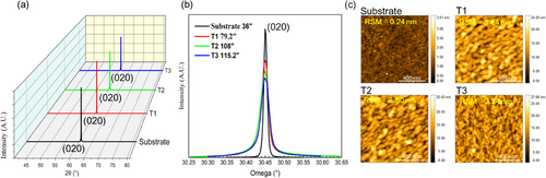
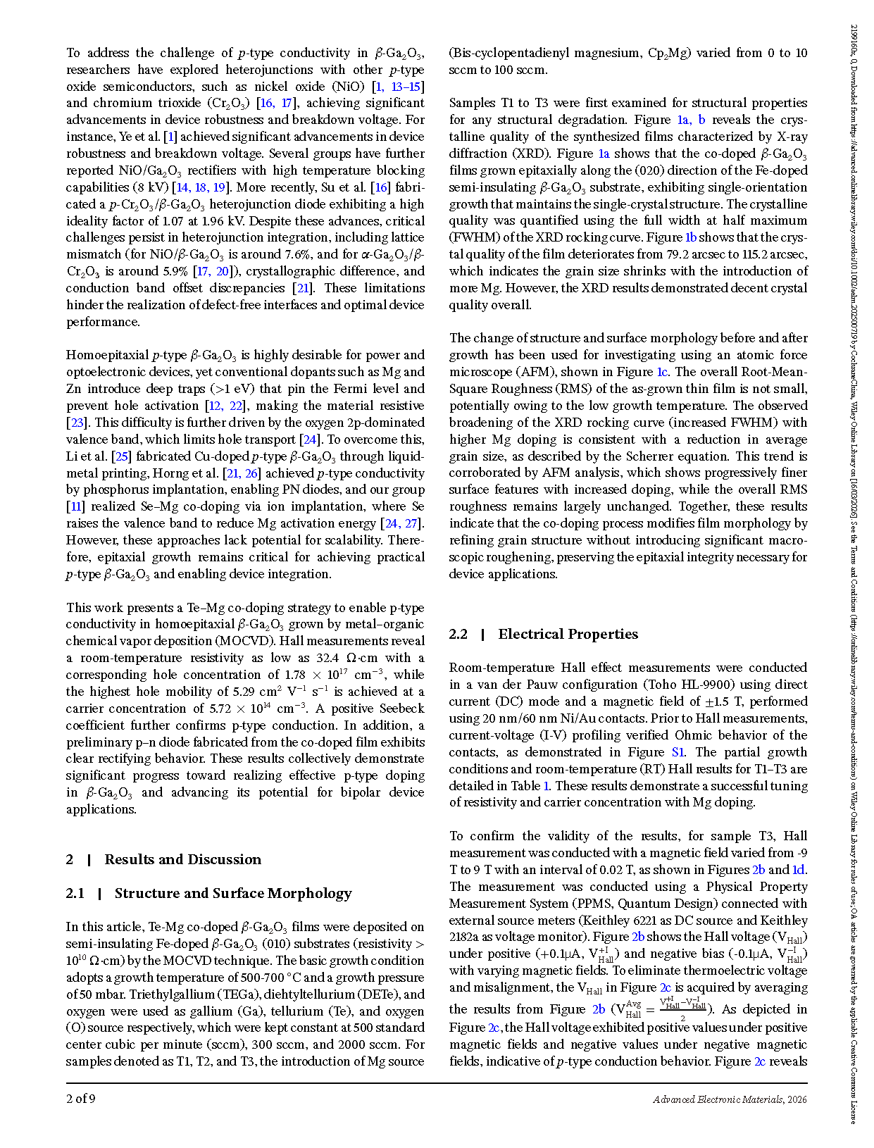
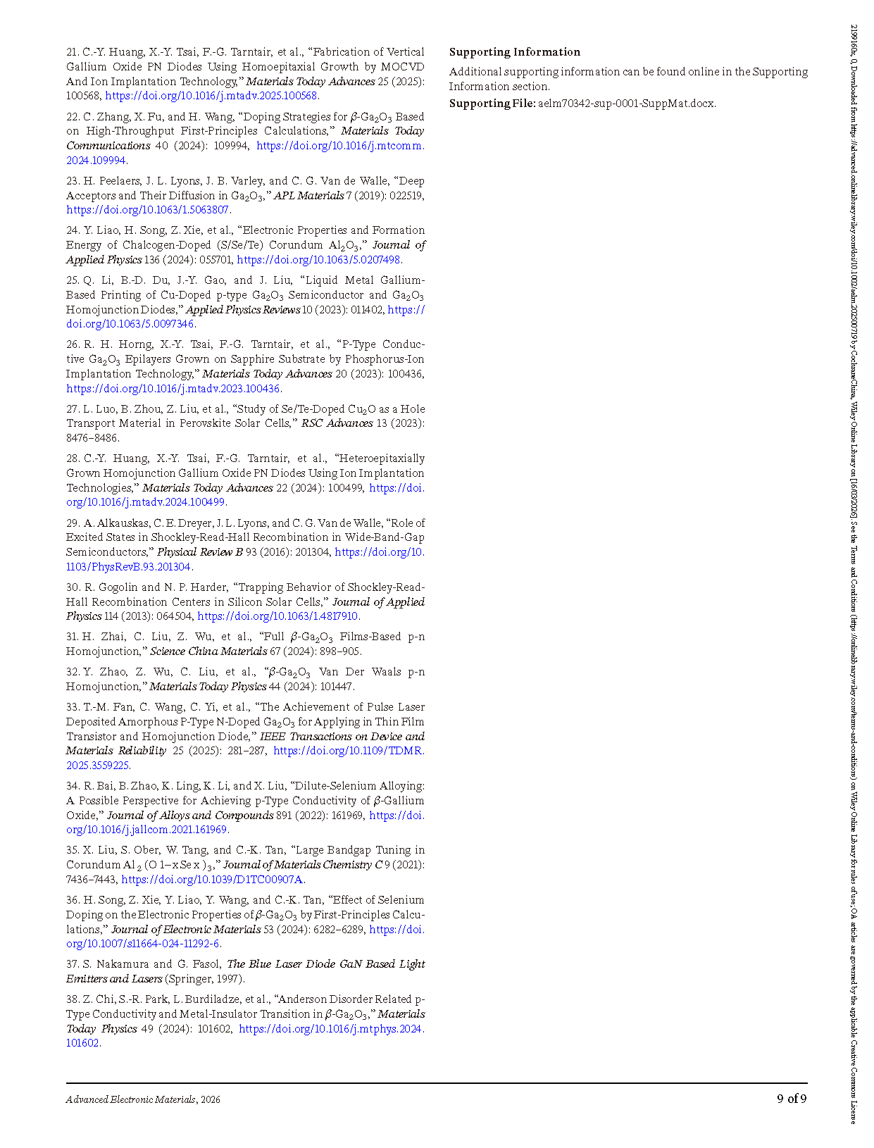
FIGURE 1. (a)XRD 2θ-ω scan. (b)XRD rocking curve. (c)Surface topography (1 µm × 1 µm) scanned by AFM for the Fe-Ga2O3 substrate and samples T1 to T3.
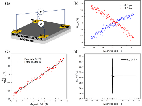
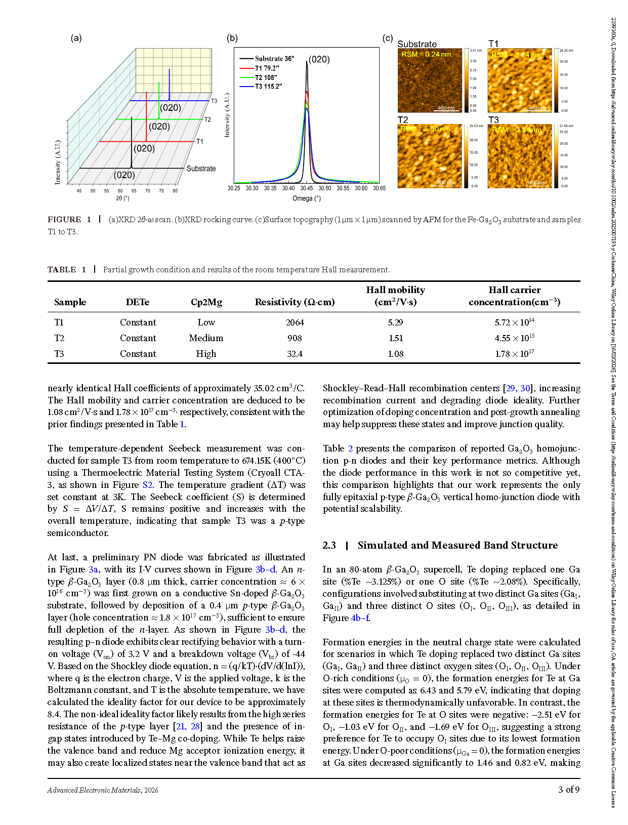
FIGURE 2. (a) Schematic demonstration of Hall measurement at van der Pauw configuration. (b) Hall voltage measured with magnetic field varying from −9 to 9 T, (c) the averaged Hall voltage, and (d) the calculated Hall coefficient for sample T3.
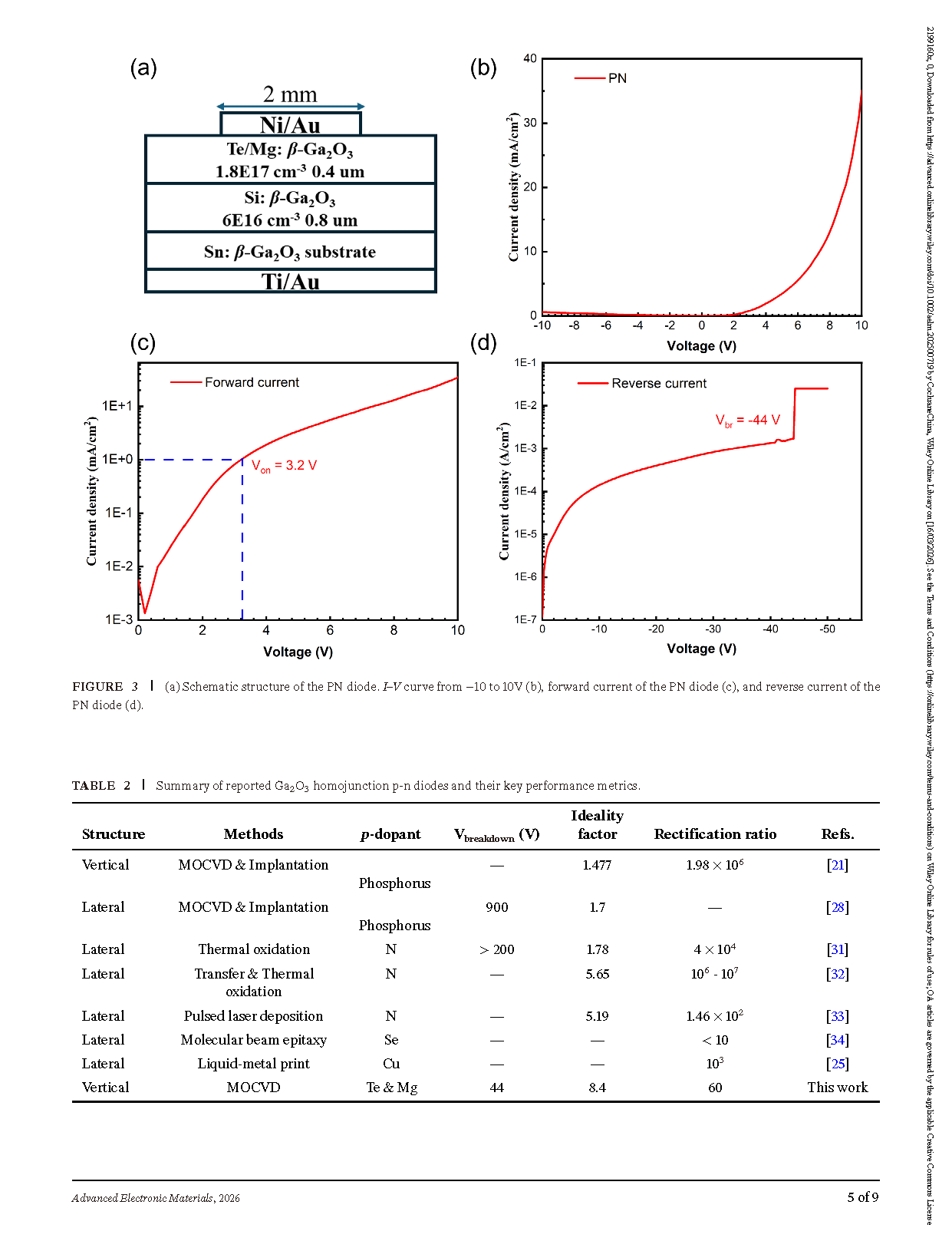
FIGURE 3. (a) Schematic structure of the PN diode. I–V curve from −10 to 10V (b), forward current of the PN diode (c), and reverse current of the PN diode (d).
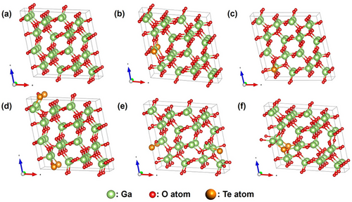
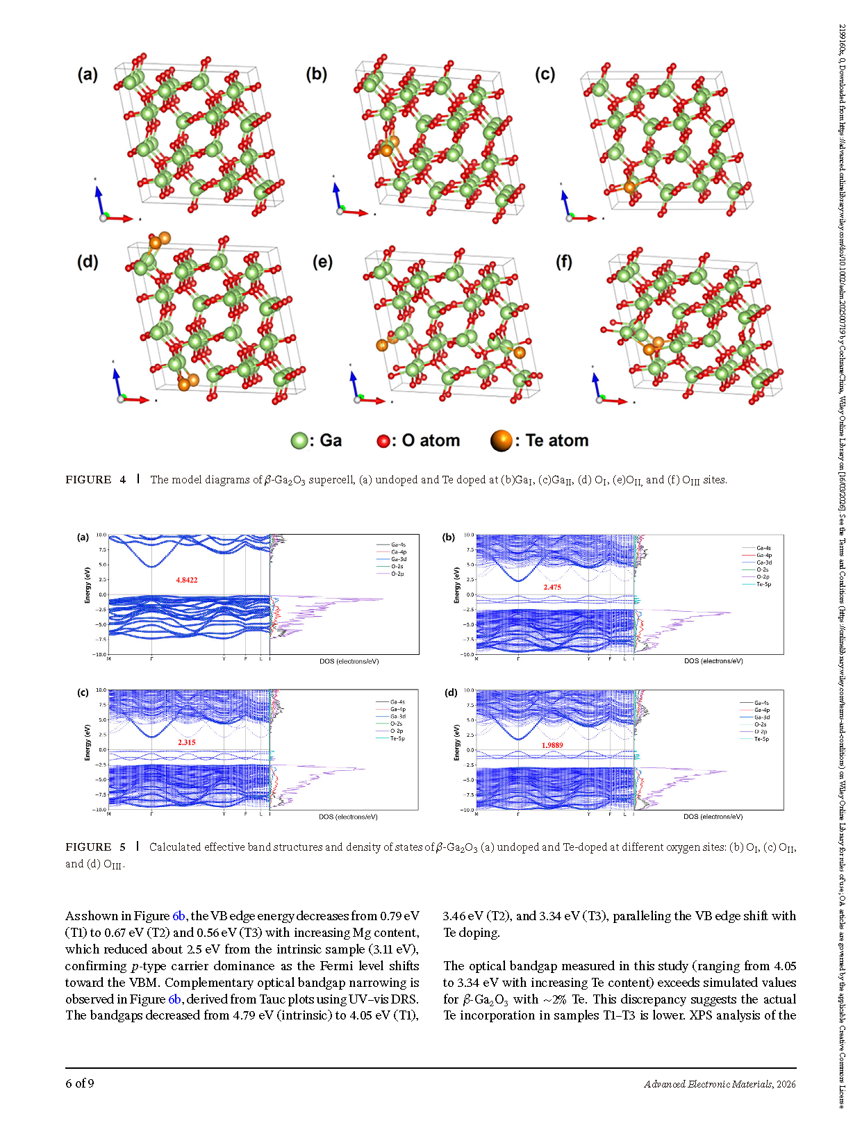
FIGURE 4. The model diagrams of β-Ga2O3 supercell, (a) undoped and Te doped at (b)GaI, (c)GaII, (d) OI, (e)OII, and (f) OIII sites.
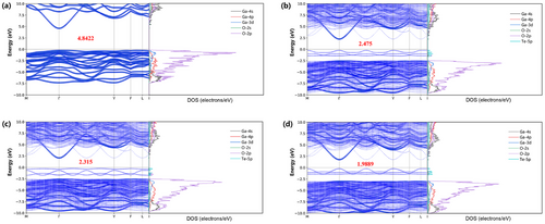
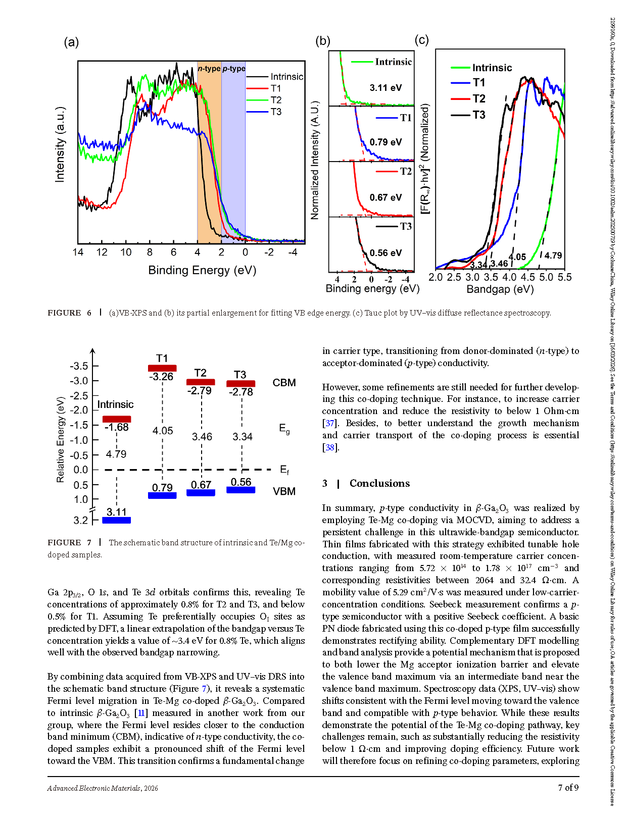
FIGURE 5. Calculated effective band structures and density of states of β-Ga2O3 (a) undoped and Te-doped at different oxygen sites: (b) OI, (c) OII, and (d) OIII.
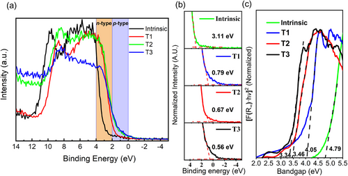
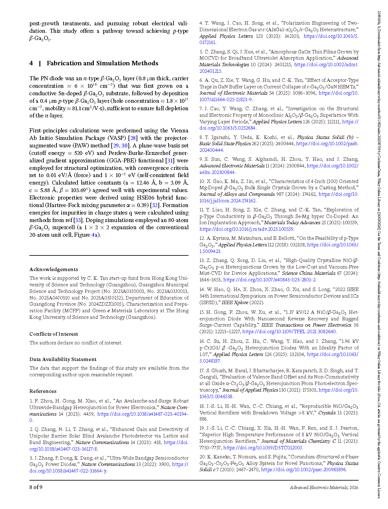
FIGURE 6. (a)VB-XPS and (b) its partial enlargement for fitting VB edge energy. (c) Tauc plot by UV–vis diffuse reflectance spectroscopy.
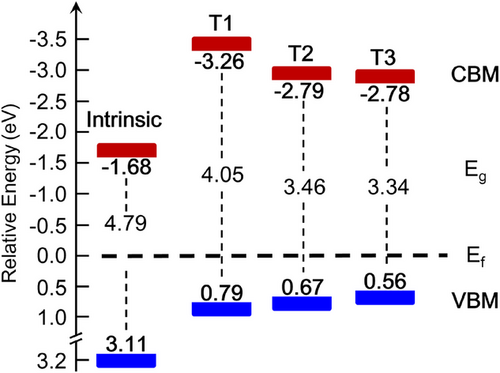
FIGURE 7. The schematic band structure of intrinsic and Te/Mg co-doped samples.
DOI:
doi.org/10.1002/aelm.202500719