Paper Sharing
【International Papers】Double drift layers to minimize on-resistance in 2.7-kV β-Ga₂O₃ (001) vertical trench Schottky barrier diodes
日期:2026-03-20阅读:222
Researchers from the University of Bristol have published a dissertation titled " Double drift layers to minimize on-resistance in 2.7-kV β-Ga2O3 (001) vertical trench Schottky barrier diodes " in Applied Physics Letters.
Background
Ultra-wide bandgap beta-gallium oxide (β-Ga2O3) has attracted significant attention for high-voltage power electronics, owing to its high critical electric field that supports kilovolt-class operation. Vertical Ga2O3 power devices typically employ a few-micrometer-thick drift layer on conductive substrates, across which most of the voltage is dropped when the device is in the off-state. These drift layers are lightly or unintentionally doped (UID) to allow for a wide depletion extension, reducing the electric field and enabling high breakdown voltages (Vbr). However, in two-terminal devices, such as vertical Ga2O3 planar Schottky barrier diodes (SBDs), the electric field peaks at the Schottky metal/Ga2O3 interface, leading to thermionic emission-driven reverse leakage currents that severely limit breakdown voltage and thus off-state device performance. Trench Schottky barrier diodes (TSBDs) overcome this limitation by leveraging the reduced surface field (RESURF) effect. This improvement, however, comes at the expense of specific on-resistance (Ron,sp), as trench etching and dielectric shielding of the trench sidewalls/bottom reduce the effective area of the Schottky contact to the Ga2O3 semiconductor material [the device schematic is shown in Fig. 1(a)]. In this work, we introduce a double drift layer (DDL) TSBD design that relaxes this trade-off between Ron,sp and Vbr by selectively increasing the conductivity of fin regions through Si ion implantation, which reduces Ron,sp while maintaining a low doping density in the drift region and thus not having a negative impact on Vbr. The DDL architecture minimizes Ron,sp by 46% compared to the conventional single-UID drift layer TSBD without compromising Vbr, resulting in ∼2× improvement in the Baliga's figure of merit (BFOM). We also show that the RESURF effect is more pronounced in DDL devices, with Baliga's figure of merit (BFOM) increasing by ∼160× from planar to trench SBDs, compared to only a ∼7× improvement observed for similar devices with a single UID-drift layer.
Abstract
Improved specific on-resistance (Ron,sp) in beta-gallium oxide (β-Ga2O3) trench Schottky barrier diodes (TSBDs) is achieved without the usual trade-off of reduced breakdown voltage, enabled through the use of a double drift layer (DDL) TSBD architecture; this incorporates a Si-doped drift layer atop an unintentionally doped (UID) drift region. DDL TSBDs show a 46% reduction in Ron,sp compared to single-UID drift layer TSBDs, while maintaining a similar Vbr of 2.6–2.7 kV. As a result, the DDL TSBD design enhances Baliga's figure-of-merit from 481 MW/cm2 for conventional TSBDs to 959 MW/cm2, marking a twofold improvement. Silvaco TCAD simulations further confirm that both structures exhibit similar dominant peak electric fields at the trench corners, consistent with their comparable breakdown voltages. While reducing fin width in TSBDs enhances Vbr because of an improved reduced surface field effect, we demonstrate that this effect is significantly amplified in DDL TSBDs, enabling a substantial shift in the conventional Ron,sp–Vbr trajectory.
Conclusion
In summary, we demonstrated a double drift layer (DDL) architecture that redefines the balance between specific on-resistance (Ron,sp) and breakdown voltage (Vbr) in trench Schottky barrier diodes (TSBDs). By selectively doping the top of the fin regions, the DDL TSBDs achieve a much lower Ron,sp compared to conventional single drift layer TSBDs, while maintaining a high Vbr. In contrast to single drift layer devices, where Vbr improvements come with a substantial penalty in Ron,sp, the DDL design shifts the Ron,sp–Vbr trajectory, achieving a 2× higher BFOM by efficiently managing the breakdown-limiting electric fields. This demonstrates that fin doping, rather than geometry alone, can be used to engineer the performance of vertical Ga2O3 TSBDs.
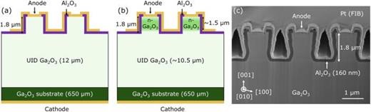
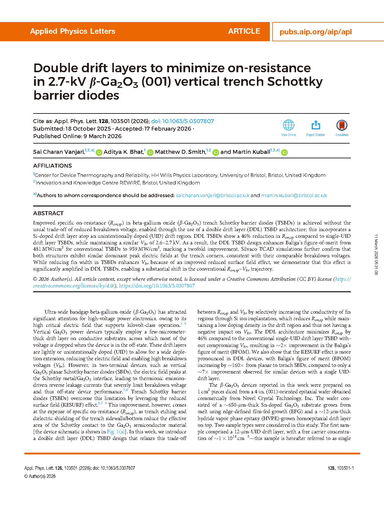
FIG. 1. Schematics of (a) a Ga2O3 trench Schottky barrier diode (TSBD) on a single drift layer (SDL) structure with a 12-μm unintentionally doped (UID) Ga2O3 drift layer and (b) a double drift layer (DDL) TSBD, where the upper 1.5 μm of the 12-μm UID drift layer is Si-doped to form a lightly doped n-type Ga2O3 region. (c) A cross section SEM image of a fabricated DDL TSBD with 1 μm fin width.
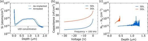
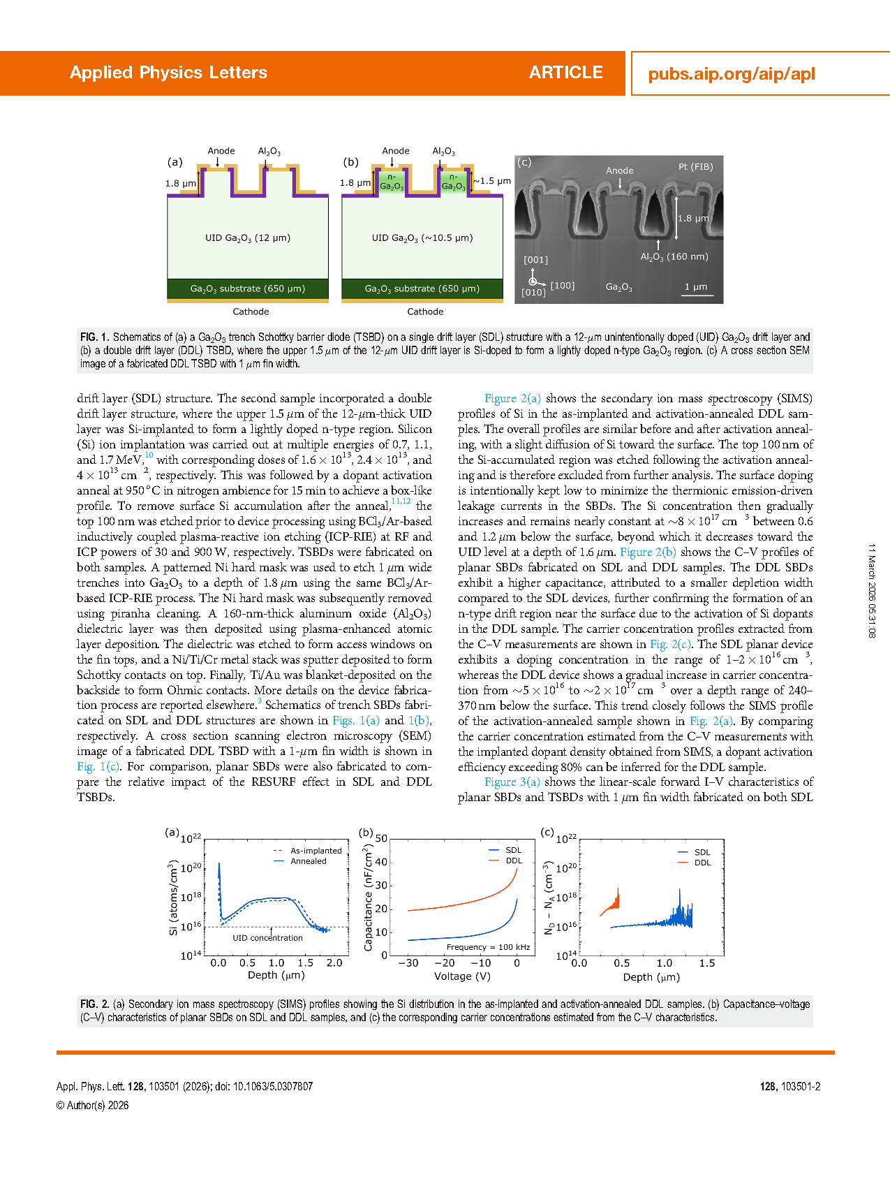
FIG. 2. (a) Secondary ion mass spectroscopy (SIMS) profiles showing the Si distribution in the as-implanted and activation-annealed DDL samples. (b) Capacitance–voltage (C–V) characteristics of planar SBDs on SDL and DDL samples, and (c) the corresponding carrier concentrations estimated from the C–V characteristics.
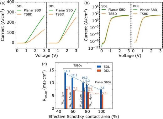
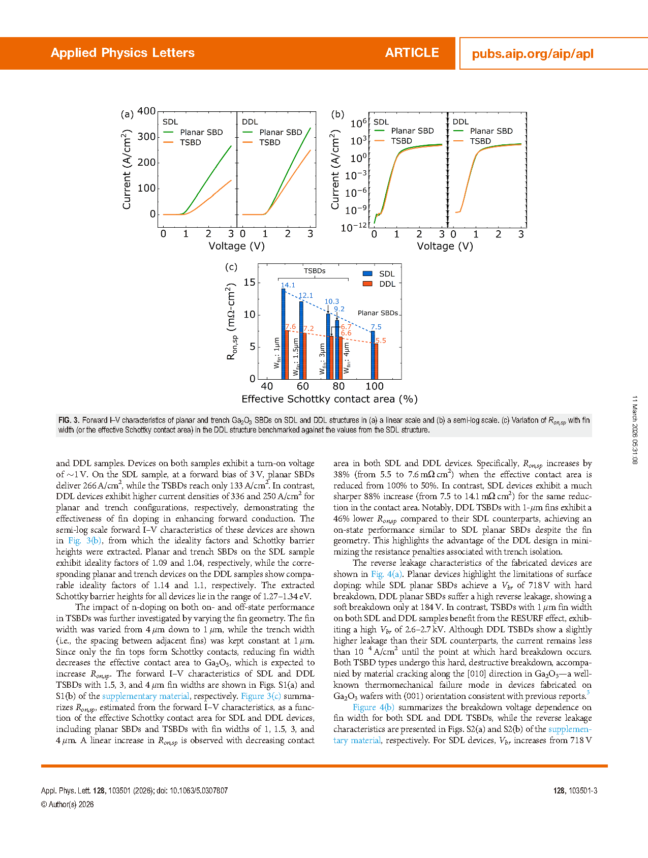
FIG. 3. Forward I–V characteristics of planar and trench Ga2O3 SBDs on SDL and DDL structures in (a) a linear scale and (b) a semi-log scale. (c) Variation of Ron,sp with fin width (or the effective Schottky contact area) in the DDL structure benchmarked against the values from the SDL structure.
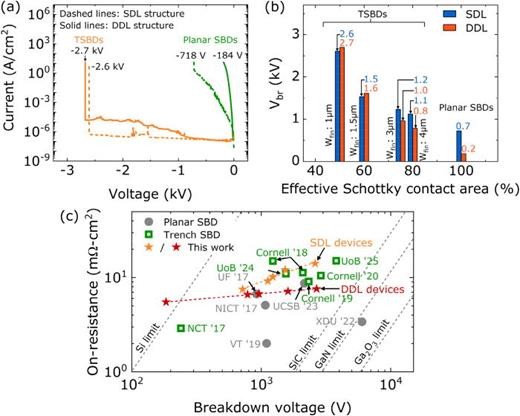
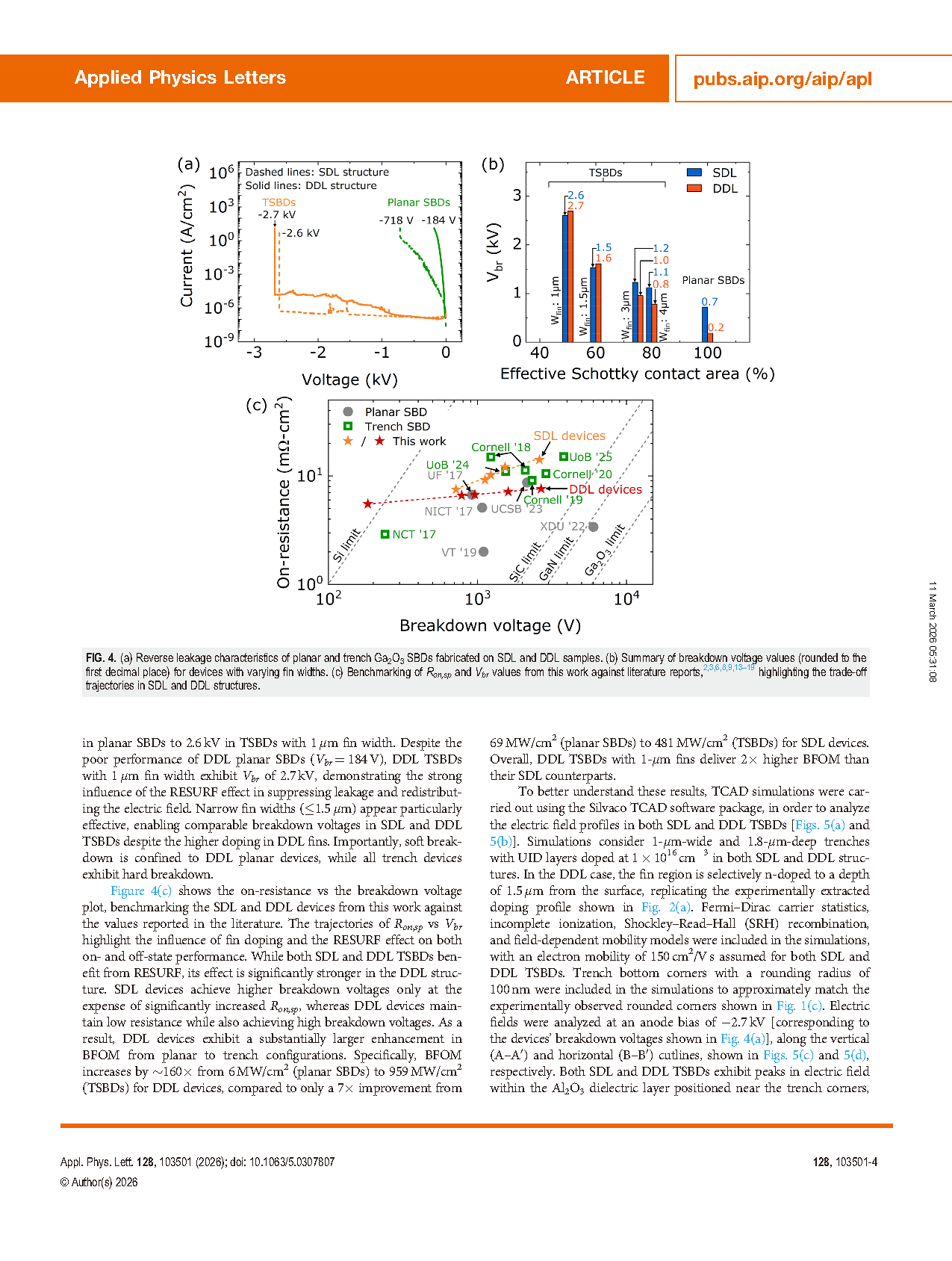
FIG. 4. (a) Reverse leakage characteristics of planar and trench Ga2O3 SBDs fabricated on SDL and DDL samples. (b) Summary of breakdown voltage values (rounded to the first decimal place) for devices with varying fin widths. (c) Benchmarking of Ron,sp and Vbr values from this work against literature reports, highlighting the trade-off trajectories in SDL and DDL structures.
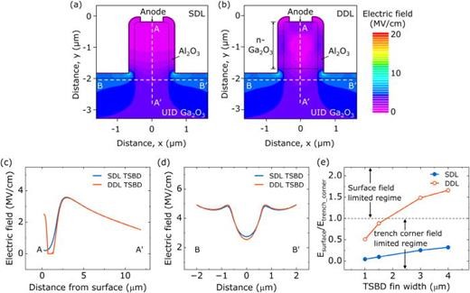
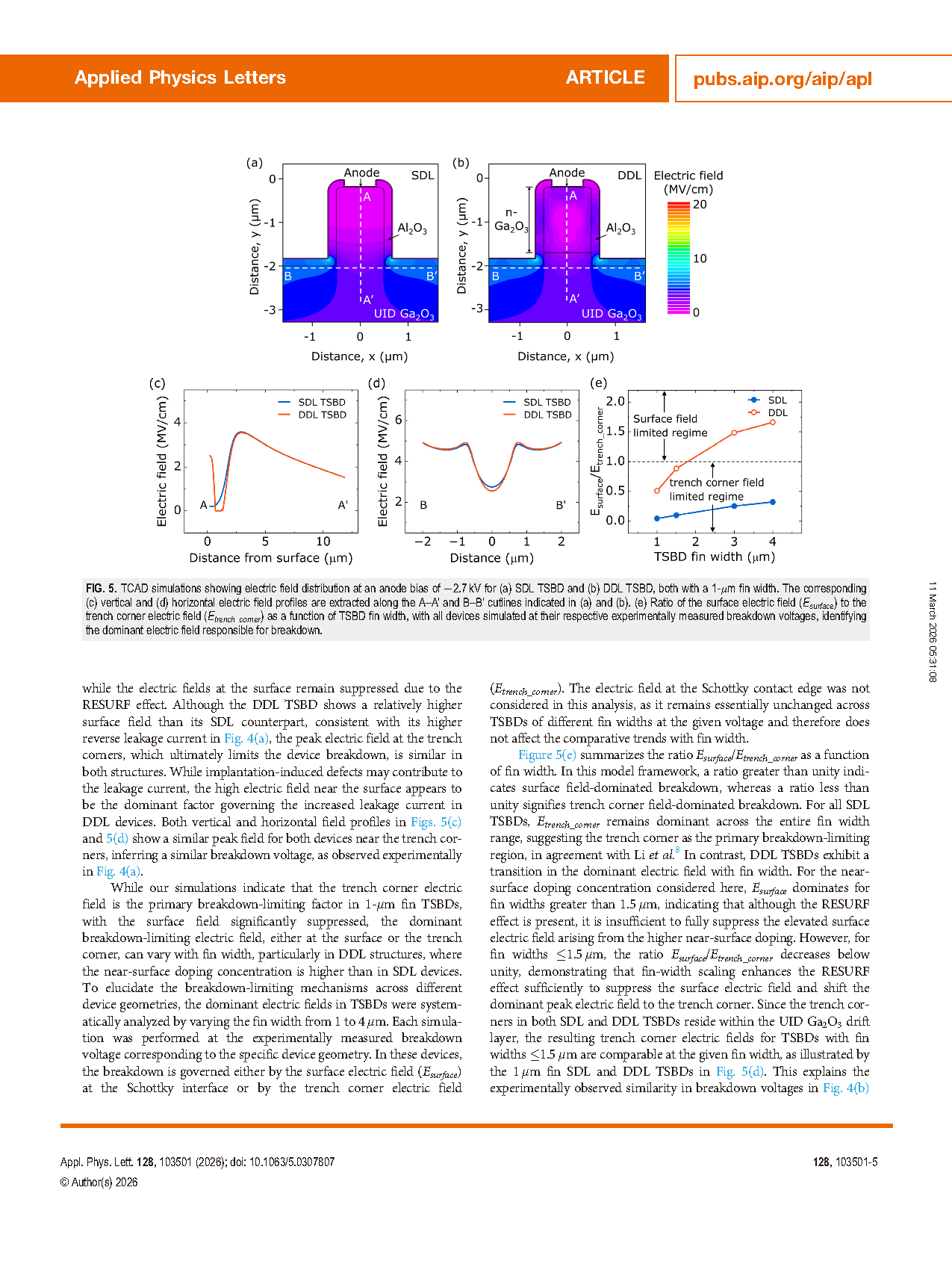
FIG. 5. TCAD simulations showing electric field distribution at an anode bias of −2.7 kV for (a) SDL TSBD and (b) DDL TSBD, both with a 1-μm fin width. The corresponding (c) vertical and (d) horizontal electric field profiles are extracted along the A–A' and B–B' cutlines indicated in (a) and (b). (e) Ratio of the surface electric field (Esurface) to the trench corner electric field (Etrench_corner) as a function of TSBD fin width, with all devices simulated at their respective experimentally measured breakdown voltages, identifying the dominant electric field responsible for breakdown.
DOI:
doi.org/10.1063/5.0307807