Paper Sharing
【Member Papers】Preparation and Properties of Wafer-Level Nanoporous GaN-Based N-Doped β-Ga₂O₃ Solar-Blind Photodetectors
日期:2026-03-20阅读:228
Researchers from the Xi’an Polytechnic University have published a dissertation titled "Preparation and Properties of Wafer-Level Nanoporous GaN-Based N-Doped β-Ga2O3 Solar-Blind Photodetectors" in Crystal Growth & Design.
Project Support
This work was supported by the Support Program for Outstanding Young Talents in Shaanxi Higher Education Institutions, China; the Key Research and Development Program of Shaanxi Province, China (2025CY-YBXM-052); the Science and Technology Project of Xi’an City, China (25GXKJRCO0069); the “Scientists + Engineers” Team Project of Xianyang City, China (L2024-CXNL-KJRCTDDWJS-0008); the Technology Innovation Guidance Project of Shaanxi Province, China (2025ZC-YYDP-30; 2025ZC-YYDP39); the Innovation and Entrepreneurship Training Program for College Students, China (S202510709118); the Key Project of the Education Department of Shaanxi Province, China (25JP069); the “Scientists + Engineers” Team Project of Shaanxi Province, China; and the Special Program for Cultivating Undergraduate Students’ Representative Achievements of Xi’an Polytechnic University (2025bzcg20).
Background
β-Ga2O3 has emerged as a research hotspot in the field of solar-blind PDs due to its advantages, such as a wide bandgap (4.9 eV), high breakdown electric field, excellent stability, and simple fabrication process. Owing to its high precision and strong sensitivity, β-Ga2O3 solar-blind PDs are widely applied in areas including fire detection, ozone hole monitoring, communication, and missile tracking. Currently, β-Ga2O3 solar-blind PDs exist in various forms, such as bulk materials, micro/nanostructures, and thin films. Among these, β-Ga2O3 thin-film metal−semiconductor-metal (MSM) solar-blind PDs have attracted extensive attention due to their simple fabrication process, excellent performance, good repeatability, and broad application scenarios. However, a large number of oxygen vacancies exist in β-Ga2O3 thin films. Acting as recombination centers, these oxygen vacancies usually lead to a large dark current and slow response speed of the device, thereby significantly degrading device performance.
Abstract
Wafer-level nanoporous GaN-based N-doped β-Ga2O3 (NP-GaN/N-Ga2O3) solar-blind photodetectors (PDs) are prepared by electrochemical etching and pulsed laser deposition. NP-GaN/N-Ga2O3 thin films with various N-doping concentrations exhibit the structure with [−201] orientation. After N doping, the defect-related photoluminescence (PL) intensity of NP-GaN/N-Ga2O3 is significantly weakened, indicating that N doping causes the transition of β-Ga2O3 thin films from a direct bandgap to an indirect bandgap. As the N-doping concentration increases, the defect-related PL intensity of NP-GaN/N-Ga2O3 becomes weaker due to the decreased defect density in β-Ga2O3 thin films. Compared with as-grown GaN-based N-doped β-Ga2O3 (AG-GaN/N-Ga2O3), NP-GaN/N-Ga2O3 has a weaker PL intensity, which is due to the fact that the stress relaxation and reduced defect density of NP-GaN improve the crystal quality of β-Ga2O3 thin films. The epitaxial relationship of β-Ga2O3 (−201) || GaN (0001) with β-Ga2O3 [010] || GaN [−12–10] is proved. Compared with undoped β-Ga2O3 PDs, N-doped β-Ga2O3 PDs have lower dark currents and shorter rise/decay times, which is due to the fact that N-doping reduces the density of oxygen vacancies.
Conclusions
Wafer-level nanoporous GaN-based N-doped β-Ga2O3 (NPGaN/N-Ga2O3) solar-blind PDs have been successfully fabricated via a new process. Structural characterization confirms that NP-GaN/N-Ga2O3 with varying N-doping concentrations maintains a monoclinic β-Ga2O3 structure with a [−201] orientation, and the epitaxial relationship βGa2O3 (−201) || GaN (0001) with β-Ga2O3 [010] || GaN [−12−10] is verified. The defect-related PL intensity of NPGaN/N-Ga2O3 is significantly weakened, indicating a direct-toindirect bandgap transition via N-induced band structure modification. Higher N-doping concentrations further reduce the defect-related PL intensity of NP-GaN/N-Ga2O3 due to the decreased defect density of the β-Ga2O3 thin film. Compared to AG-GaN/N-Ga2O3, NP-GaN/N-Ga2O3 exhibits weaker defect-related PL intensity, attributed to stress relaxation and increased crystal quality in the nanoporous GaN. N-doped PDs show lower dark currents and shorter rise/ decay times compared with undoped PDs, originating from Ndoping-induced reduction of oxygen vacancies.
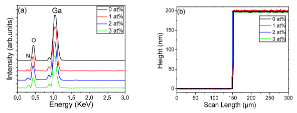
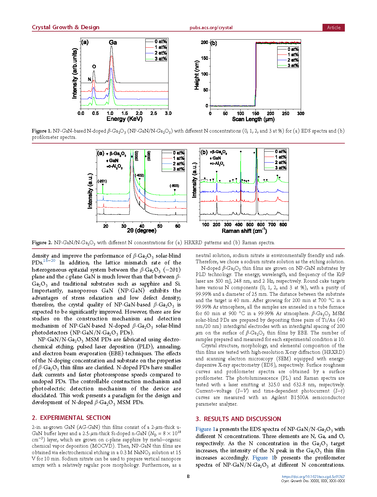
Figure 1. NP-GaN-based N-doped β-Ga2O3 (NP-GaN/N-Ga2O3) with different N concentrations (0, 1, 2, and 3 at %) for (a) EDS spectra and (b) profilometer spectra.
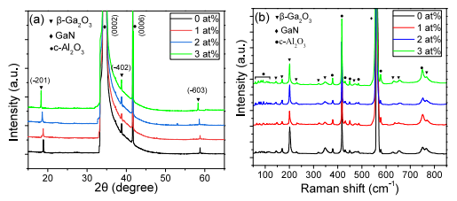
Figure 2. NP-GaN/N-Ga2O3 with different N concentrations for (a) HRXRD patterns and (b) Raman spectra.
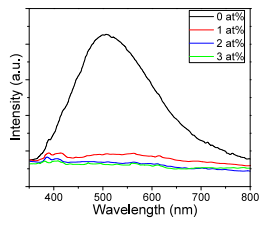
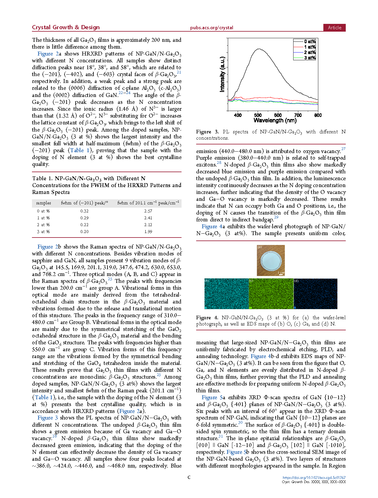
Figure 3. PL spectra of NP-GaN/N-Ga2O3 with different N concentrations.
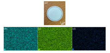
Figure 4. NP-GaN/N-Ga2O3 (3 at %) for (a) the wafer-level photograph, as well as EDS maps of (b) O, (c) Ga, and (d) N.
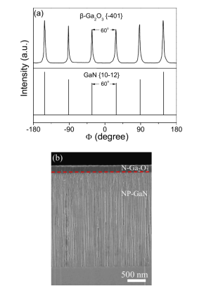
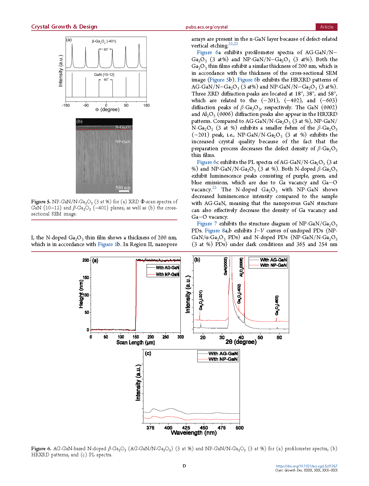
Figure 5. NP-GaN/N-Ga2O3 (3 at %) for (a) XRD Φ-scan spectra of GaN {10−12} and β-Ga2O3 {−401} planes, as well as (b) the cross-sectional SEM image.
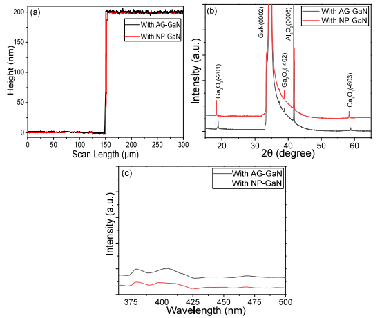
Figure 6. AG-GaN-based N-doped β-Ga2O3 (AG-GaN/N-Ga2O3) (3 at %) and NP-GaN/N-Ga2O3 (3 at %) for (a) profilometer spectra, (b) HRXRD patterns, and (c) PL spectra.
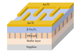
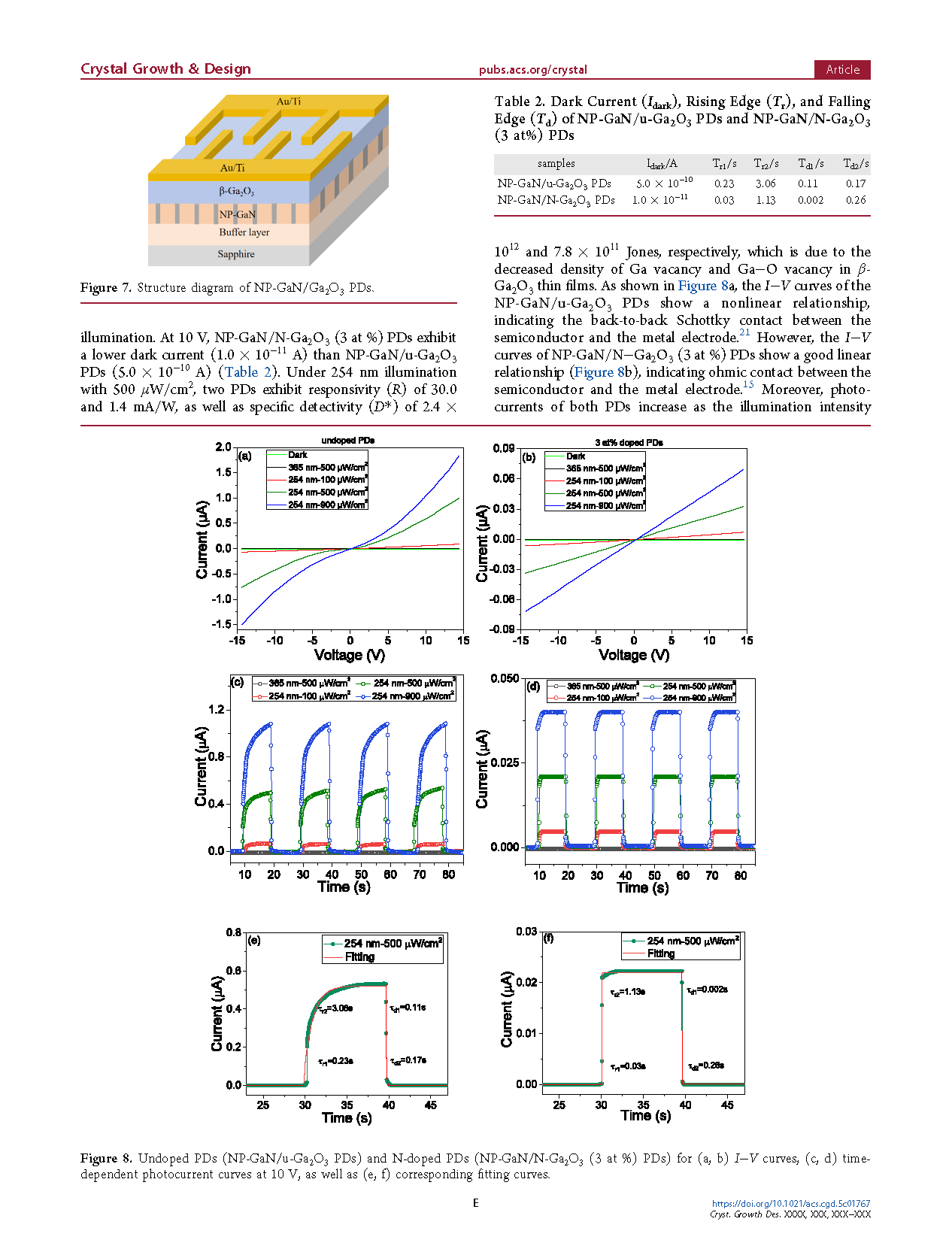
Figure 7. Structure diagram of NP-GaN/Ga2O3 PDs.
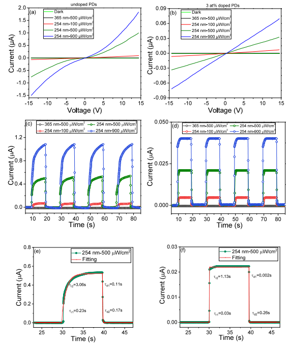
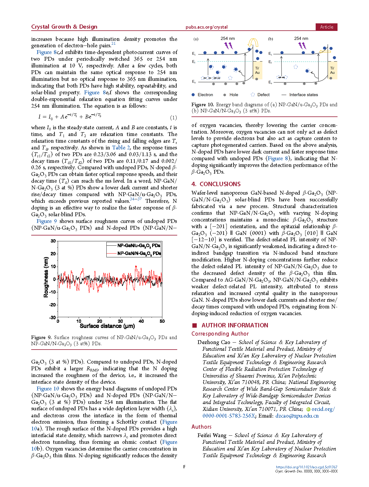
Figure 8. Undoped PDs (NP-GaN/u-Ga2O3 PDs) and N-doped PDs (NP-GaN/N-Ga2O3 (3 at %) PDs) for (a, b) I−V curves, (c, d) time-dependent photocurrent curves at 10 V, as well as (e, f) corresponding fitting curves.
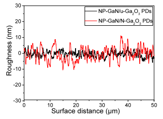
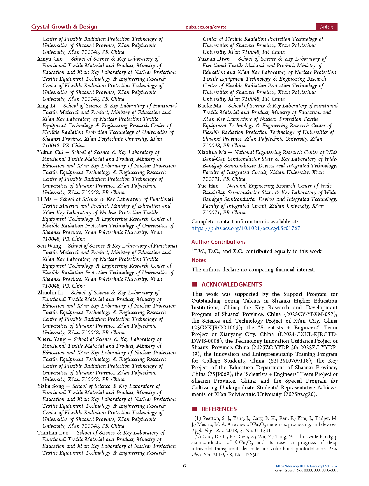
Figure 9. Surface roughness curves of NP-GaN/u-Ga2O3 PDs and NP-GaN/N-Ga2O3 (3 at%) PDs.
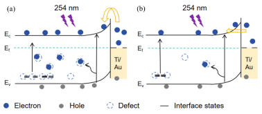
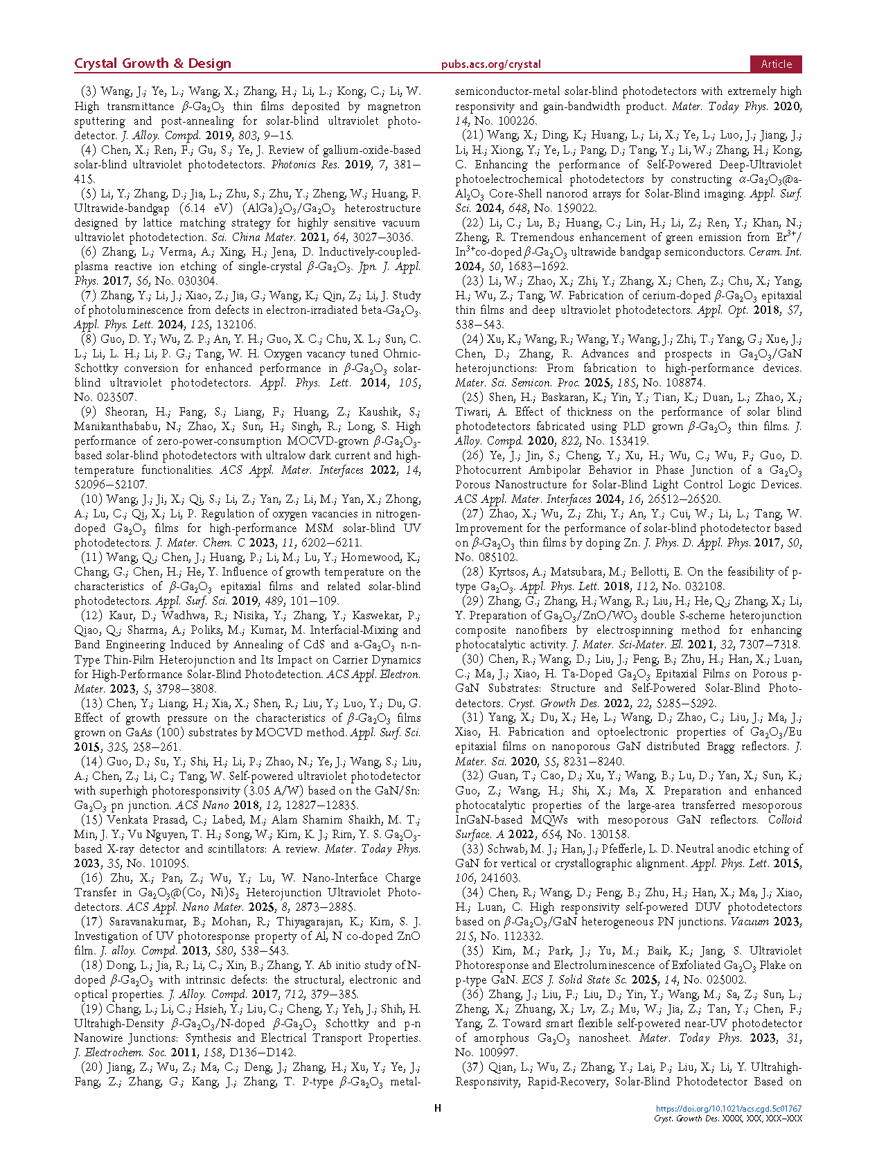
Figure 10. Energy band diagrams of (a) NP-GaN/u-Ga2O3 PDs and (b) NP-GaN/N-Ga2O3 (3 at%) PDs.
DOI:
doi.org/10.1021/acs.cgd.5c01767