


Patents
【Patents】Global Gallium Oxide Patent Landscape: From Japan’s Early Leadership to a China–Japan Duopoly
日期:2026-03-20阅读:1472
After third-generation semiconductor materials such as silicon carbide (SiC) and gallium nitride (GaN), the ultra-wide bandgap semiconductor Gallium Oxide is gradually emerging as a next-generation key material attracting global attention. In particular, China’s Outline of the 15th Five-Year Plan for National Economic and Social Development explicitly lists Gallium Oxide and diamond among the ultra-wide bandgap semiconductors as key frontier materials, signaling that Gallium Oxide has moved from a long-term research hotspot into the core focus of the country’s strategic new materials system.
Compared with SiC and GaN, Gallium Oxide has a wider bandgap, which theoretically enables a higher breakdown field and lower power loss. Additionally, Gallium Oxide single crystals can be grown directly using the melt method, making the production of large-size substrates at relatively low cost feasible. Therefore, Gallium Oxide is considered to have significant application potential in ultra-high-voltage power electronic devices and solar-blind ultraviolet photodetectors.
As breakthroughs in material growth and device technology continue, the development of Gallium Oxide is gradually transitioning from the early-stage fundamental research phase toward the initial commercialization stage. According to market research firm DataIntelo, the global Gallium Oxide market is expected to reach approximately USD 450 million by 2032. As one of the fourth-generation semiconductor materials advancing industrialization relatively quickly, Gallium Oxide has become an important technological focus in the global semiconductor field.
Major science and technology nations and regions are continuously increasing policy and R&D investments around this material system. In Japan, the Semiconductor and Digital Industry Strategy published in 2021 identifies Gallium Oxide as a key area for support, aiming to maintain technological leadership. China, in its 14th Five-Year Plan and the National Strategic Emerging Industries Development Plan, proposes forward-looking deployment in frontier materials such as wide-bandgap semiconductors, conducting R&D on critical technologies including large-size single-crystal substrate production, high-quality epitaxial growth, power devices, and solar-blind ultraviolet photodetectors. Meanwhile, the United States also considers Gallium Oxide an emerging technology of strategic significance and included it in export control regulations in 2022.
In this context, patent data serve as an important window to observe technological development and industrial competition. Patents not only record technological innovations but also reflect the R&D layout of companies and research institutions, target markets, and technological pathway choices. Systematic analysis of patent data allows a clearer understanding of the development stage of a technology, the main competitive players, and the core technological directions.
Based on this, this article provides a systematic review and analysis of global Gallium Oxide-related patents. The data were sourced from the Himmpat patent database and obtained through combined searches using Chinese and English keywords along with IPC classification codes, with the retrieval cutoff date of December 1, 2025. After data cleaning, deduplication, and family consolidation, a total of 3,317 patent applications were obtained. On this basis, the article conducts a systematic analysis of global technological development in Gallium Oxide.
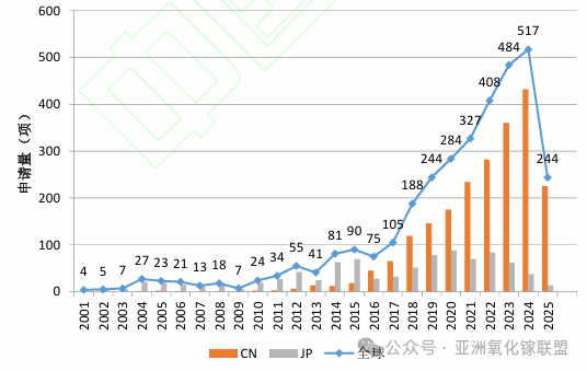
Global Patents Enter a Phase of Rapid Growth
From the perspective of patent application trends, the development of Gallium Oxide technology can be roughly divided into three stages:
Stage 1: Early Exploration (before 2004)
During this period, research was mainly focused on exploring crystal growth methods and investigating the physical properties of the material. At that time, Gallium Oxide was not widely recognized as a next-generation power semiconductor material, and related research was limited in scale. The number of global patent applications per year was typically fewer than 10, with the field remaining largely at the fundamental research stage.
Stage 2: Technological Breakthrough (2004–2013)
After 2004, Japan took the lead in increasing R&D investment in Gallium Oxide and gradually established a systematic patent portfolio. During this stage, Japan achieved a series of key breakthroughs in material growth and device research. For example, the successful growth of 2-inch β-Gallium Oxide single crystals and laboratory validation of Gallium Oxide power devices were accomplished. These results marked the point at which Gallium Oxide began to demonstrate feasibility for power device applications and laid the technical foundation for subsequent industrialization.
Stage 3: R&D Diffusion and Initial Industrialization (2014–present)
In 2014, the number of global patent applications reached 81 for the first time, representing an important turning point in technology diffusion. That year, patent filings saw a clear increase, and the upward trend continued in subsequent years. By 2024, the annual number of global patent applications had exceeded 500.
As the technological potential of Gallium Oxide became increasingly validated, countries such as China and the United States rapidly ramped up R&D investment, making Gallium Oxide a major focus in the global semiconductor field. Currently, both China and Japan have achieved commercial supply of 2–4 inch Gallium Oxide substrates and epitaxial wafers. Performance of related power diodes and MOSFET devices continues to improve, with these devices gradually entering application verification stages, and the prospects for industrialization are becoming increasingly clear.
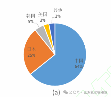
Global Competitive Landscape: China and Japan as the Dual Leaders
From the perspective of patent technology origins, Gallium Oxide technology is mainly concentrated in China, Japan, South Korea, the United States, and Europe. Among these, China and Japan represent the core global innovation forces.
China accounts for approximately 64% of the patents, already holding a clear advantage in quantity, making it the largest source of Gallium Oxide technology worldwide. Japan accounts for around 25%; although its patent count is lower than China’s, it still maintains clear advantages in key core technologies and foundational aspects of the industrial chain.
Particularly in upstream materials, Japanese companies have accumulated deep expertise in Gallium Oxide single-crystal substrates and epitaxial materials, giving them strong industrial control. Many key technological breakthroughs were first achieved by Japanese research institutions and enterprises.
Overall, the global Gallium Oxide technology landscape has gradually shifted from Japan’s absolute early dominance to a competitive dual-leader pattern with China. In contrast, South Korea, the United States, and Europe remain relatively limited in patent numbers and technological accumulation, currently mainly at the follow-up stage.
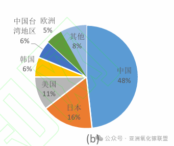
China Becomes the Largest Patent Target Market
From the perspective of patent target markets, China has become the most important region for Gallium Oxide patent deployment worldwide.
The global distribution of major patent target markets is approximately as follows:
China: ~48%
Japan: ~16%
United States: ~11%
China’s position as the largest target market can be attributed to two main factors. On one hand, Chinese innovators typically prioritize filing patents domestically, resulting in a larger number of local patents. On the other hand, as one of the world’s largest semiconductor application markets, China is highly attractive to international companies, many of which choose to deploy patents in China to facilitate future market entry.
In contrast, Japanese companies place more emphasis on patent deployment in overseas markets such as China and the United States, while Chinese innovators have relatively limited patent presence in Japan. This, to some extent, reflects the differences between the two countries in terms of internationalization of intellectual property strategies.
Major Global Innovators
From the ranking of global patent applicants, among the top 15, China accounts for 8 while Japan accounts for 7, indicating that the competition in Gallium Oxide technology is mainly concentrated between these two countries.
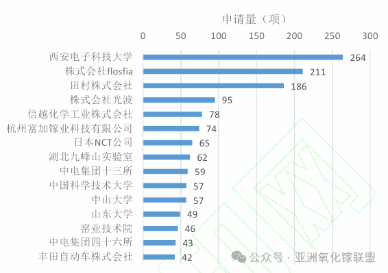
The top three institutions form the first tier:
Xidian University
Flosfia Inc.
Tamura Co., Ltd.
These institutions are clearly ahead of other applicants in terms of patent volume. The team led by Academician Hao Yue at Xidian University has long focused on high-quality Gallium Oxide epitaxy, as well as innovation in power and RF devices. They have achieved key breakthroughs in the controllable epitaxial growth of high-quality β-Gallium Oxide thin films, and their power diodes and RF devices have reached world-class performance. Japan’s Flosfia Inc. focuses on the α-Gallium Oxide technology route, utilizing its self-developed Mist-CVD technology to produce high-quality Gallium Oxide films and achieving a series of device performance breakthroughs. By 2025, the company completed technical verification for 4-inch wafer manufacturing, placing it at the forefront of industrialization worldwide. Tamura Co., Ltd., an early pioneer in Gallium Oxide technology, achieved laboratory validation of Gallium Oxide power devices as early as 2012 and laid the foundation for controllable β-Gallium Oxide epitaxial wafer preparation. Through a spin-off, Novel Crystal Technology, Inc. (NCT) was established to specifically drive Gallium Oxide industrialization and is regarded as a key force in bringing Gallium Oxide materials to large-scale production.
In the second tier, Japanese companies also stand out. Kohwa Co., Ltd., Shin-Etsu Chemical Co., Ltd., and NCT rank 4th, 5th, and 7th, respectively. Kohwa Co., Ltd. is the core supplier of HVPE equipment in Japan’s Gallium Oxide industry chain; Shin-Etsu Chemical Co., Ltd. focuses on providing complete epitaxial wafer solutions; NCT specializes in Gallium Oxide single-crystal substrate development and commercialization and is currently the main supplier of commercial Gallium Oxide substrates.
Chinese company Hangzhou Fujia Gallium Technology Co., Ltd. (Fujia Gallium) ranks 6th globally with 74 patent applications and is a major driver of Gallium Oxide material industrialization in China. The company has achieved significant breakthroughs in large-size single-crystal growth, MOCVD epitaxy, and vertical Bridgman (VB) growth equipment, and has already started building China’s first 6-inch Gallium Oxide single-crystal and epitaxial wafer production line. Other Chinese institutions on the list are universities or research institutes, including Jiufengshan Laboratory (JFS), CETC 13th Research Institute, CETC 46th Research Institute, University of Science and Technology of China (USTC), Sun Yat-sen University (SYSU), and Shandong University (SDU). These institutions play key roles in basic research and tackling critical technologies: CETC 46th Research Institute has achieved consecutive breakthroughs in 2-, 4-, and 6-inch Gallium Oxide single-crystal growth in China, while Sun Yat-sen University (SYSU) successfully developed China’s first large-size Gallium Oxide single-crystal thin-film heteroepitaxy MOCVD equipment.
It is worth noting that the innovation systems of China and Japan show clear differences. Chinese institutions on the list are mainly universities and research institutes, indicating that Gallium Oxide R&D in China is currently driven primarily by national research projects and cutting-edge academic exploration, and is at a critical stage transitioning from laboratory breakthroughs to industrial-scale applications. In contrast, all the Japanese entities are companies, showing that their technological innovation is more market-driven, with closer integration of R&D and industrialization. Japan has now formed a complete industrial chain loop—from basic materials and specialized equipment to device applications—creating high entry barriers for full-chain development that China and other followers need to overcome.
Core Technology Routes
From the distribution of patents, the Gallium Oxide industry technology system has already formed a relatively clear technology chain, mainly covering four key segments: single-crystal growth, substrate processing, epitaxial growth, and device fabrication.
Single-Crystal Growth
Single-crystal growth is the upstream core technology in the Gallium Oxide industry chain and one of the directions with the densest patent activity. Currently, Gallium Oxide crystal growth mainly involves techniques such as the floating-zone method (FZ), Czochralski method (CZ), edge-defined film-fed growth (EFG), vertical Bridgman (VB), and casting methods.
In the early research stage, Japan held a clear advantage in this field. For example, Waseda University first achieved β-Gallium Oxide single-crystal growth using the floating-zone method. Subsequently, Kohwa Co., Ltd. improved the thermal conductivity of the crystal and stabilized the crystal growth interface by adding specific dopants to the raw materials. Nippon Light Metal Co., Ltd. reduced the resistivity of Gallium Oxide single crystals by doping with SnO₂.
Regarding the Czochralski method, Japanese companies also explored early on. For example, Kohwa Co., Ltd. enhanced crystal purity by adding impurity-removal units to the growth apparatus. Chinese research institutions then carried out a series of improvements. Shandong University installed cylindrical post-heaters on iridium crucibles to effectively suppress Gallium Oxide volatilization and decomposition during high-temperature growth. Hangzhou GAREN Semiconductor achieved large-size, high-quality single-crystal growth through a dual-zone temperature structure and thermal shielding design.
Currently, the most widely applied growth technique is the edge-defined film-fed growth (EFG) method. This method was first proposed and industrialized by Japanese companies. For instance, Adamant Namiki Precision Jewel Co., Ltd. achieved batch production of 2-inch Gallium Oxide single crystals around 2010, making EFG the mainstream Gallium Oxide crystal growth technology. Later, Tamura Co., Ltd. continuously optimized mold structures, temperature-field control, and crystal-defect suppression.
Chinese research institutions have also made important progress in this technology direction. For example, Shanghai Institute of Optics and Fine Mechanics, Chinese Academy of Sciences successfully grew Gallium Oxide crystals using the EFG method while effectively suppressing bubbles and polycrystalline formation. CETC 46th Research Institute achieved stable growth of large-size Gallium Oxide crystals by optimizing thermal field structures. Hangzhou Fujia Gallium Technology Co., Ltd. has also explored introducing artificial intelligence into the crystal growth process for process parameter optimization.
To reduce crystal growth costs, vertical Bridgman (VB) methods have received increasing attention in recent years. For example, Shinshu University achieved low-cost Gallium Oxide crystal growth using Pt-Rh alloy crucibles. Novel Crystal Technology, Inc. (NCT) further optimized VB growth quality through dopant concentration control and equipment structure improvements. Chinese companies, such as Fujia Gallium and Hangzhou GAREN Semiconductor, are also actively exploring this growth method.
Additionally, some research institutions have proposed new crystal fabrication routes. For instance, Hangzhou Global Scientific and Technological Innovation Center and Hangzhou GAREN Semiconductor proposed growing columnar single crystals directly via directional solidification casting to reduce equipment complexity and production costs. Nanjing Tongli Crystal Materials Research Institute and Beijing Gachuang Technology Co., Ltd. explored cold-crucible crystal growth using water-cooled copper crucibles to avoid the use of expensive iridium crucibles.
Substrate Processing
After obtaining Gallium Oxide single crystals, they need to be processed into high-quality substrates through cutting, grinding and polishing, and cleaning. The quality of substrate processing directly affects epitaxial layer growth and device performance, making it an important focus of patent activity.
In terms of cutting technology, Tamura Co., Ltd. proposed creating multiple rows of laser-modified regions to form a layered embrittlement structure, combined with mechanical cutting processes. This approach effectively addresses the low processing efficiency caused by the cleavage-prone nature of Gallium Oxide crystals.
Regarding grinding and polishing, several institutions have proposed novel processing methods. For example, Yancheng Institute Of Technology proposed an “anti-cleavage suspension polishing slurry,” which suppresses microcrack propagation during processing through special additives. The Japanese materials company Fujimi Corporation developed a water-based polishing system combining specific abrasive particle sizes with acidic modifiers to improve polishing efficiency and surface flatness.
Additionally, Xidian University proposed using photo catalytically assisted chemical mechanical polishing (CMP) technology to reduce polishing time and minimize surface roughness.
For cleaning technology, Fujimi Corporation developed a high-concentration surfactant cleaning system to achieve low-damage surface cleaning. The Chinese company Beijing Jiazu Technology proposed a multi-step chemical cleaning process combined with ultrasonic treatment to obtain highly clean wafer surfaces.
Epitaxial Growth
Epitaxial growth is a critical step for realizing Gallium Oxide device structures. Currently, the main Gallium Oxide epitaxial techniques include HVPE, MOCVD, MBE, and Mist-CVD.
In terms of HVPE technology, Japanese companies and universities hold a leading position. For example, Tamura Co., Ltd. and Tokyo University of Agriculture and Technology were early to achieve large-diameter, high-quality β-Gallium Oxide epitaxial film growth. In subsequent studies, they optimized gas-phase reaction conditions to increase growth rates and improve surface quality. Novel Crystal Technology, Inc. (NCT) further enhanced the electrical performance of epitaxial wafers through annealing treatments and defect-control techniques.
Chinese companies have also made progress in this area. For instance, Beijing Migsemi Semiconductor achieved controlled growth of phase-pure β-Gallium Oxide thick films on sapphire substrates. CETC 46th Research Institute prepared high-quality thick epitaxial films through hydrogen pre-treatment processes.
For MOCVD technology, domestic universities have contributed multiple innovations. Dalian University of Technology reduced carbon contamination and improved film purity via hydrogen-assisted growth. Jilin University improved heteroepitaxial quality using a GaN buffer layer and a temperature-gradient epitaxy strategy. Tokyo University of Agriculture and Technology and Taiyo Nippon Sanso Corporation in Japan realized high-mobility Gallium Oxide film growth using high-temperature gas mixing techniques. Chinese company Hangzhou Fujia Gallium Technology Co., Ltd. addressed uneven heating in equipment via a laser-assisted heating structure.
Regarding MBE technology, Japanese companies conducted early research. Tamura Co., Ltd. achieved high-quality Gallium Oxide thin films by adjusting growth temperature and VI/III ratios, and precisely controlled Si doping. In China, Shanghai Institute of Optics and Fine Mechanics, Chinese Academy of Sciences obtained high-mobility films via homoepitaxy on vicinal substrates, while Changchun Institute of Optics, Fine Mechanics and Physics, CAS explored solutions to the challenges of p-type doping in Gallium Oxide.
For Mist-CVD technology, Japanese company Flosfia Co., Ltd. was the first to realize α-Gallium Oxide film fabrication and established a series of patent portfolios. Nanjing University in China prepared Cr-doped α-Gallium Oxide epitaxial films using Mist-CVD and achieved control over metastable Gallium Oxide crystal phases.
Additionally, some research institutions have explored PLD and LPCVD methods, though these have not yet become mainstream technology routes.
Device Fabrication
At the device level, Gallium Oxide is primarily applied in power devices and optoelectronic devices. Typical devices include:
Schottky barrier diodes (SBDs)
Field-effect transistors (MOSFETs / MISFETs)
Solar-blind ultraviolet photodetectors
Radio-frequency (RF) devices and gas sensors
Among these, SBD technology is the most mature. Early patents have realized Gallium Oxide SBD device structures, and subsequent research has mainly focused on improving breakdown voltage and electric field modulation. For example, Tamura Co., Ltd. formed high-resistance regions via ion implantation to improve the electric field distribution, and together with Novel Crystal Technology, Inc. (NCT) proposed trench-type SBD structures. On the domestic university side, Xidian University significantly enhanced device breakdown voltage through field-plate structures and vertical designs, while University of Science and Technology of China proposed using a p-type NiO heterostructure to form a JTE termination for improved voltage tolerance.
In terms of field-effect transistors, Japanese companies initially proposed basic MESFET structures, but due to limited gate control capability, subsequent research gradually shifted to MOSFET and MISFET structures. In recent years, research has focused on gate structure optimization and the realization of normally-off devices. For instance, composite gate structures, dual-gate designs, and trench-gate designs can simultaneously enhance gate control and reduce on-resistance. Some studies have also introduced p-type NiO gate structures combined with field-plate designs to achieve normally-off devices with both high breakdown voltage and low power consumption.
Overall, Gallium Oxide device technology remains in a rapid development stage, with power devices and ultraviolet photodetectors being the current focus of research and patent activity.
Future Development Trends
The Gallium Oxide industry is still at a critical stage of transitioning from scientific breakthroughs to large-scale applications. With improvements in material quality, maturation of epitaxial growth technologies, and continual optimization of device structures, Gallium Oxide holds broad application prospects in ultra-high-voltage power electronics, ultraviolet photodetectors, and high-frequency electronic devices.
For China, enhancing future industrial competitiveness will primarily depend on two aspects. On one hand, it is necessary to further promote enterprises as the main drivers of technological innovation, strengthening collaborative innovation among companies, universities, and research institutions to improve technology transfer efficiency. On the other hand, it is essential to expand global patent coverage and establish a more comprehensive intellectual property framework in major international markets to cope with increasingly fierce global technological competition.
As the industry chain gradually improves, Gallium Oxide is expected to achieve faster development in the coming years and become an important power semiconductor material system following SiC and GaN.
