Paper Sharing
【Domestic Papers】Tailoring Ga₂O₃ for solar-blind UV photodetectors: A comprehensive review of materials, techniques, and applications
日期:2026-04-07阅读:253
Researchers from the Beijing Jiaotong University have published a dissertation titled "Tailoring Ga2O3 for solar-blind UV photodetectors: A comprehensive review of materials, techniques, and applications" in Microelectronic Engineering.
Background
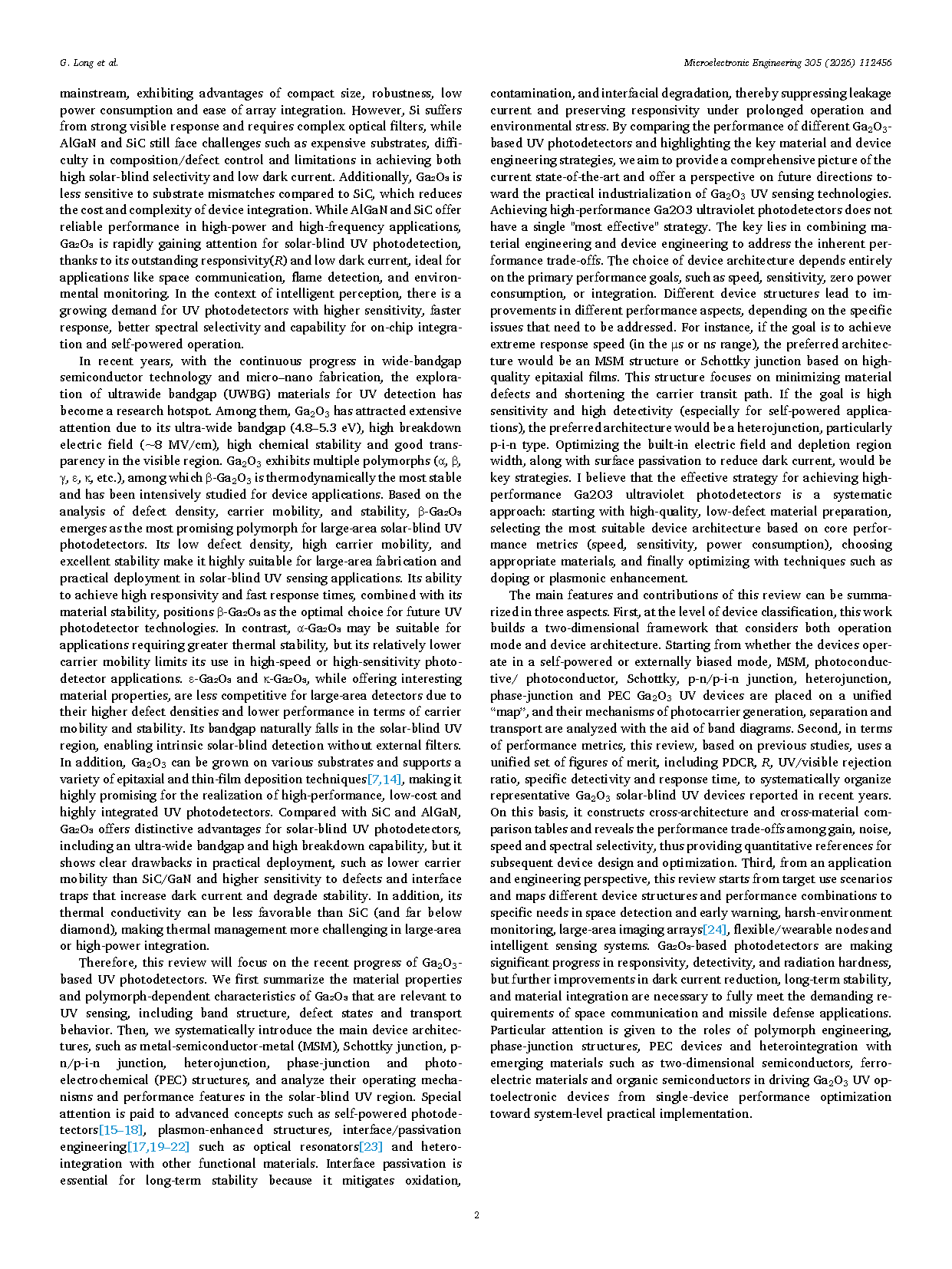
UV photodetectors are one of the most important classes of optoelectronic sensors in modern science and technology. They convert incident UV radiation into electrical signals and thereby enable non- contact, real-time monitoring of optical phenomena. In general, UV photodetectors offer advantages such as fast response, high temporal resolution, remote sensing capability and compatibility with electronic read-out circuits. Since their inception, UV-sensitive devices have become indispensable in a wide range of fields, including in environ mental monitoring, flame detection, missile early warning, space communication, sterilization process control, radiation dosimetry and biological/chemical sensing. In particular, detectors operating in the solar-blind band (200–280 nm) can distinguish artificial UV sources from the solar background, which is of great significance for high- confidence target recognition and low-false-alarm warning systems.
Abstract
Ga2O3-based ultraviolet (UV) photodetectors convert incident UV radiation into electrical signals by exploiting the strong photoresponse of ultrawide bandgap Ga2O3 ,enabling accurate UV monitoring and device control. Owing to their intrinsic solar-blind spectral response (200–280 nm), these devices hold great promise for ap plications in environmental monitoring, flame detection, space communication, missile early warning systems, and radiation sensing. Compared with traditional UV detectors such as photomultiplier tubes and Si-based devices, which suffer from bulky volume, high operating voltage, filter-dependent selectivity and strong visible- light interference, Ga2O3 photodetectors offer distinct advantages in intrinsic solar-blind selectivity, high breakdown field, low dark current, good thermal/chemical stability and compatibility with micro–nano integration. As a representative ultrawide bandgap oxide semiconductor, Ga2O3 stands out among emerging UV- sensitive materials for next-generation solar-blind detection. In this review, we summarize the development of Ga2O3-based UV photodetectors, discuss the main UV-sensitive mechanisms of Ga2O3 including band-to-band absorption, defect-related processes and internal-field-driven carrier separation, and outline recent advances in device architectures such as metal-semiconductor-metal, Schottky junction, p-n/p-i-n junction, heterojunction, phase junction and photoelectrochemical structures. By comparing the performance of Ga2O3 photodetectors with different polymorphs, growth techniques, contact schemes and interface/passivation engineering, their current application potential in various fields is analyzed. Finally, future development directions including self-powered operation, plasmon-enhanced designs, polymorph and heterostructure engineering, and large-scale integrated implementation are highlighted to provide guidance for the design and fabrication of high- performance Ga2O3 UV photodetectors.
Highlights
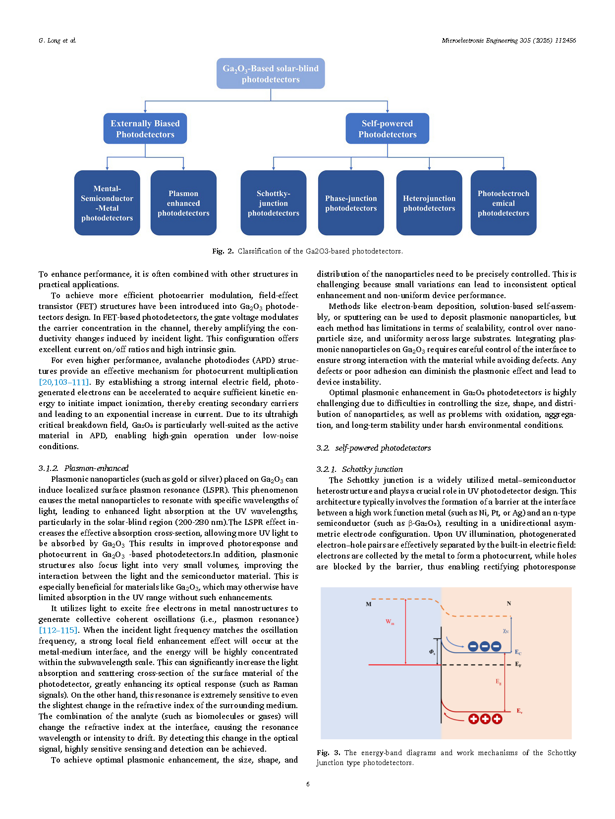
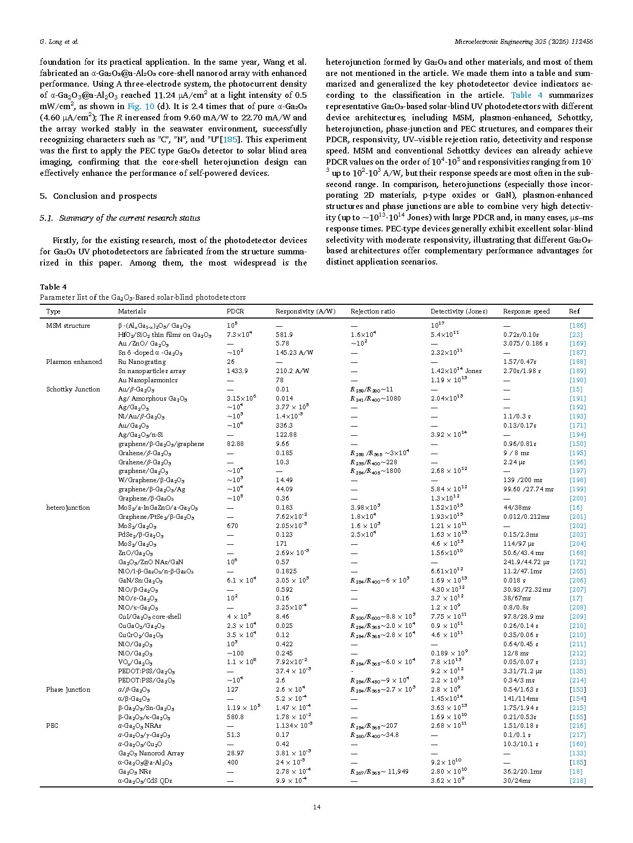
The paper innovatively establishes a two-dimensional classification system of "operation mode (self-powered/externally biased) + device architecture", integrating various Ga2O3-based detectors such as MSM, Schottky junction, p-n/p-i-n junction, heterojunction, phase junction, and PEC into a unified analytical framework.
Based on core metrics including PDCR (Photo-to-Dark Current Ratio), responsivity, UV-visible rejection ratio, specific detectivity, and response speed, the paper systematically collates the performance data of various representative devices in recent years, constructs cross-architecture and cross-material comparison tables, and quantitatively reveals the performance trade-off relationships among gain, noise, speed, and spectral selectivity.
The paper innovatively maps the combination of device structures and performance directly to specific application scenarios. For different requirements such as space detection, missile early warning, harsh environment monitoring, large-area imaging, and flexible sensing, it clarifies the adaptability and core optimization directions of various devices.
Conclusion
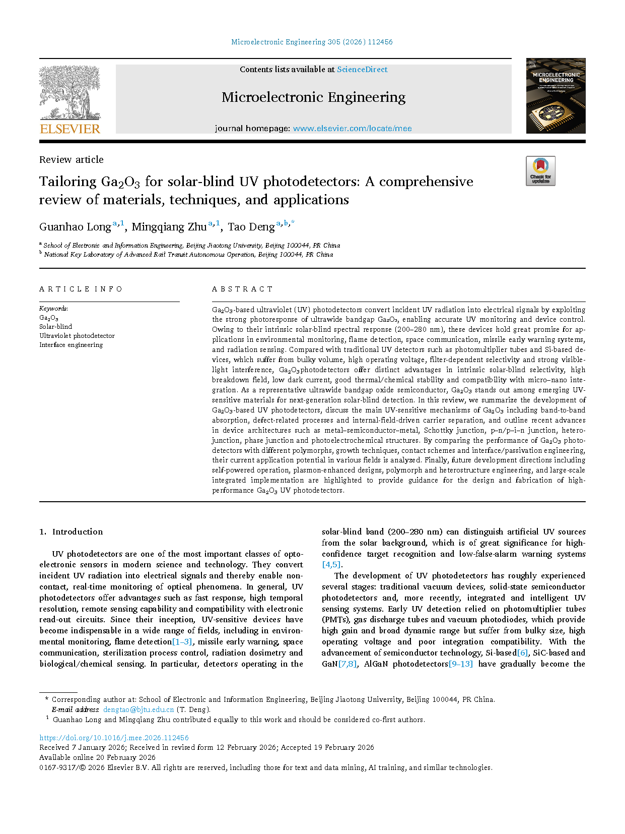
In summary, Ga2O3 -based solar-blind UV photodetectors have progressed from basic device demonstrations to a diverse family of structures, including MSM, Schottky, p–n/p–i–n, heterojunction, phase- junction and PEC configurations. Research has shown that, by optimizing crystal quality, defect states, interfaces and contact engineering, Ga2O3 devices can achieve the combination of high responsivity, low dark current, large PDCR, strong UV–visible rejection and relatively fast response, in some cases even under low bias or self-powered operation. However, several key challenges remain, such as controllable and stable p-type doping, scalable low-defect epitaxy, long-term reliability under realistic operating conditions and robust integration with readout and control electronics. Future progress will likely rely on the joint advancement of polymorph engineering, heterointegration with 2D semiconductors and P -type oxides, plasmonic and interface/passivation design, as well as system-level co-design that considers sensing, processing and communication together. With continued efforts in these areas, Ga2O3 UV photodetectors are expected to move steadily toward practical deployment in strategic applications such as space and defense, and in civilian fields including environmental monitoring, industrial safety and intelligent sensing networks.
Project Support
This work was supported by the Deep Earth Probe and Mineral Re sources Exploration-National Science and Technology Major Project (No.2024ZD1003100).
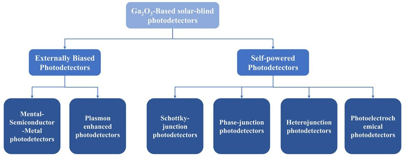
Fig. 1. Classification of the Ga2O3-based photodetectors.

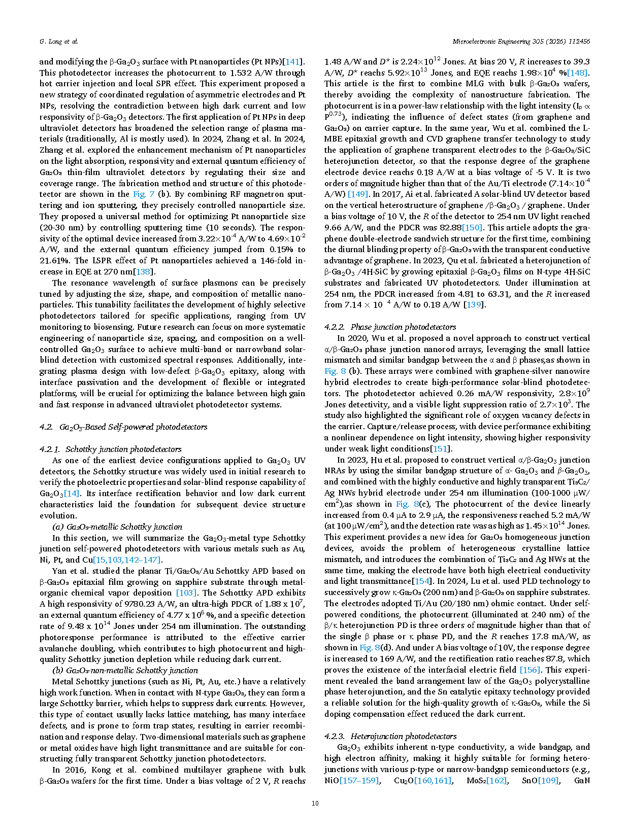
Fig. 2. (a)the schematic diagram of the Bi/β-Ga2O3/Bi UV photodetector with permission from Elsevier. (b) Pt nanoparticle size on the performance of amorphous- Ga2O3 UV detectors with permission from Elsevier. (c) Ga2O3/MLG FTO-based solar-blind UV photodetector with permission from Elsevier. (d) Interface-Engineering Ga2O3/SiC Heterojunction UV photodetectors
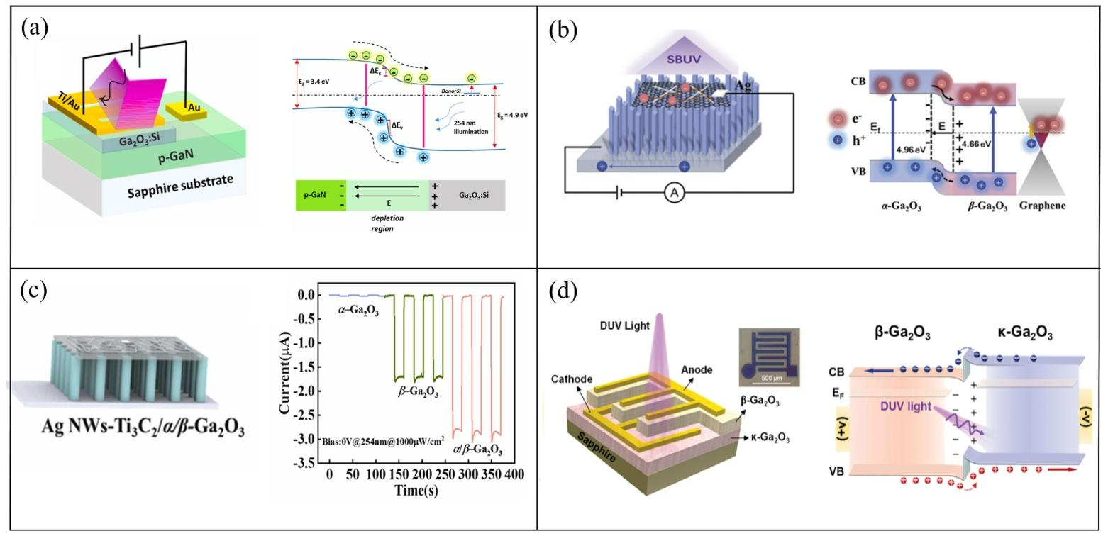
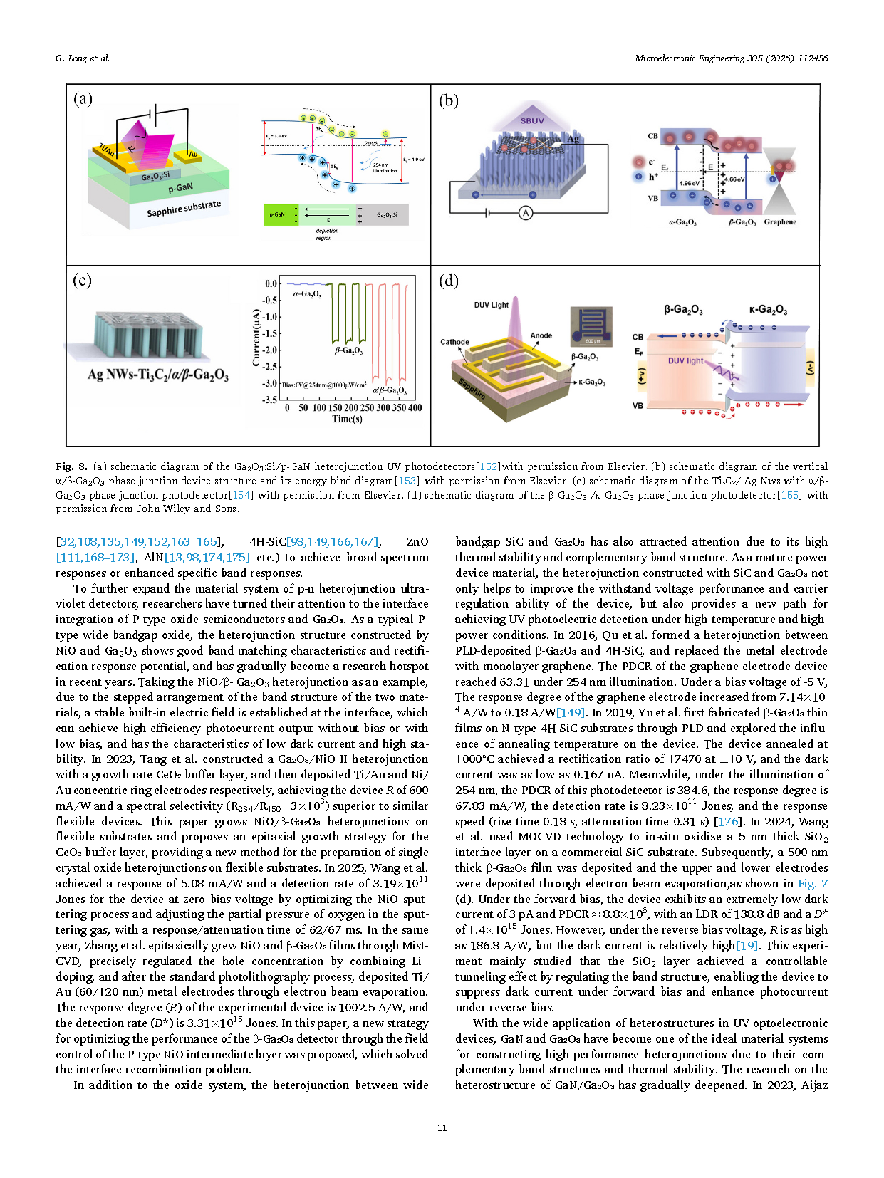
Fig. 3. (a) schematic diagram of the Ga2O3:Si/p-GaN heterojunction UV photodetectors with permission from Elsevier. (b) schematic diagram of the vertical α/β- Ga2O3 phase junction device structure and its energy bind diagram (c) schematic diagram of the Ti3C2/ Ag Nws with α/β-Ga2O3 phase junction photodetector. (d) schematic diagram of the β-Ga2O3/κ-Ga2O3 phase junction photodetector
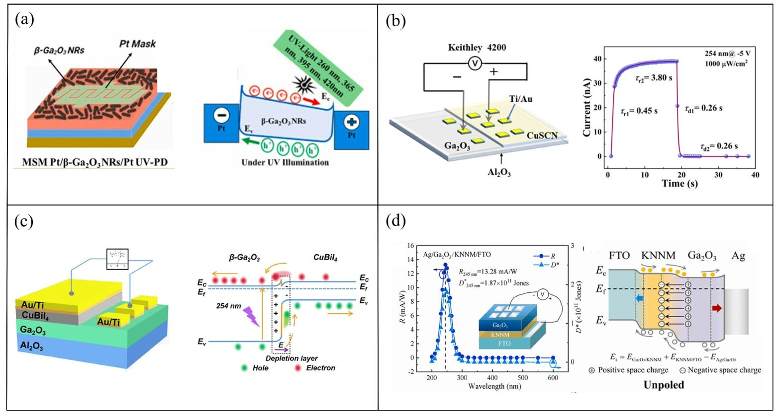
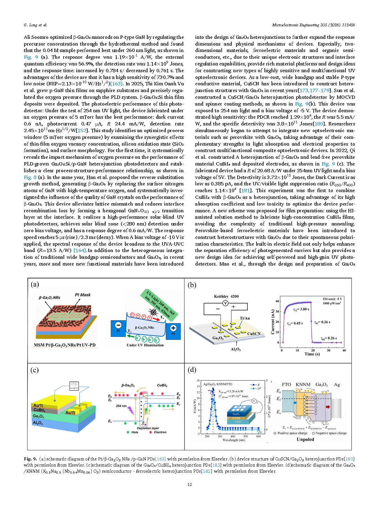
Fig. 4. (a) schematic diagram of the Pt/β-Ga2O3 NRs/p-GaN PDs with permission from Elsevier. (b) device structure of CuSCN/Ga2O3 heterojunction PDs (c) schematic diagram of the Ga2O3/CuBiI4 heterojunction PDs with permission from Elsevier. (d) schematic diagram of the Ga2O3/KNNM(K0.5Na0.5(Nb0.94Mn0.06)O3) semiconductor - ferroelectric heterojunction PDs
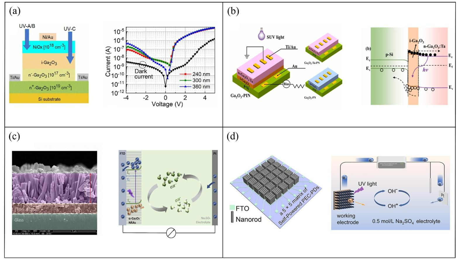
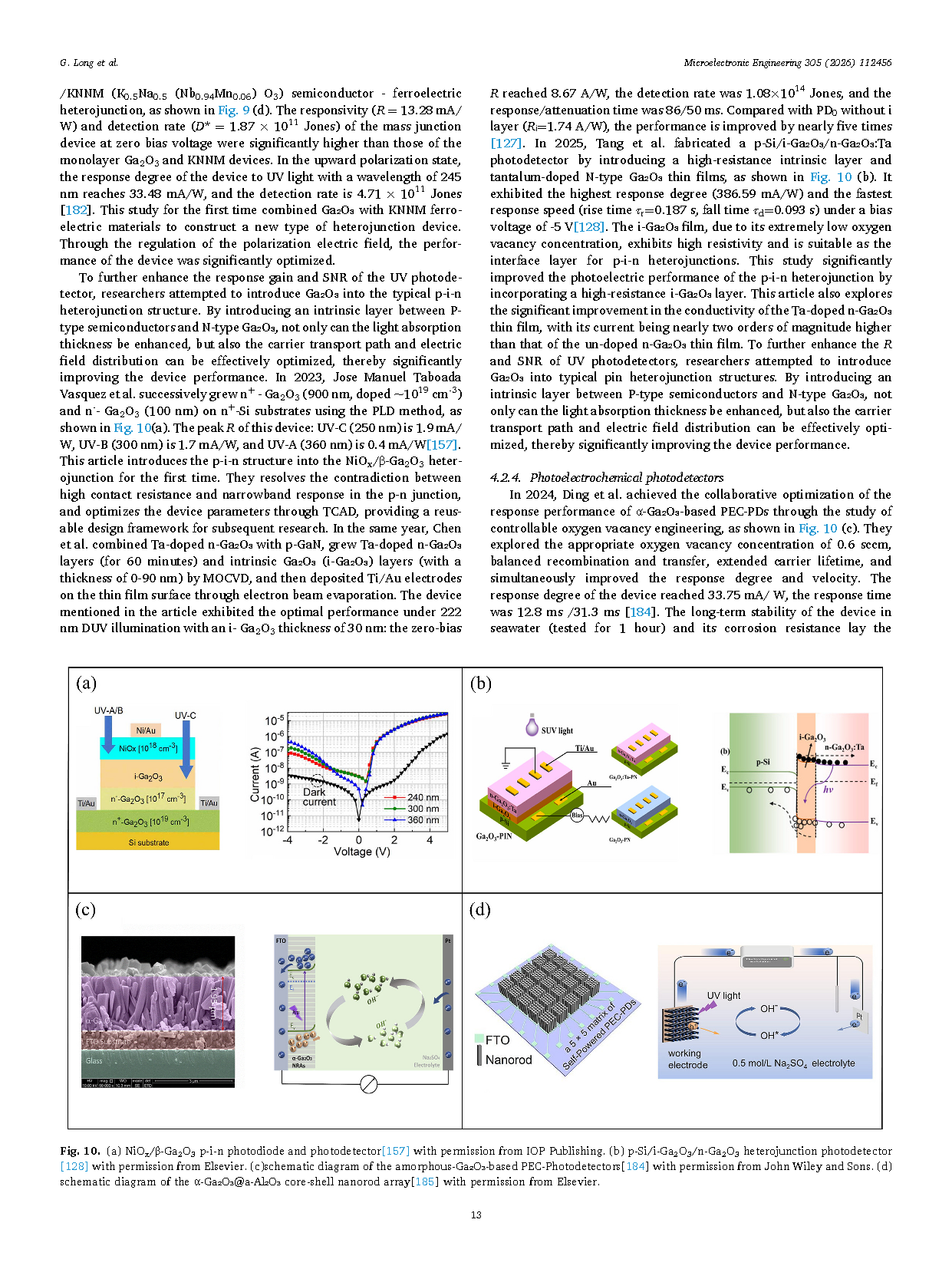
Fig.5.(a) NiOx/β-Ga2O3 p-i-n photodiode and photodetector with permission from IOP Publishing. (b) p-Si/i-Ga2O3/n-Ga2O3 heterojunction photodetector (c) schematic diagram of the amorphous-Ga2O3-based PEC-Photodetectors. (d) schematic diagram of the α-Ga2O3 @ a-Al2O3 core-shell nanorod array.
DOI:
doi.org/10.1016/j.mee.2026.112456