Paper Sharing
【International Papers】Formation of GaN-Ga₂O₃ surface heterostructures via Femtosecond-laser-irradiation for sensitive and selective NO₂ sensing at elevated temperatures
日期:2026-04-07阅读:225
Researchers from Fraunhofer Institute for Ceramic Technologies and Systems IKTS have published a dissertation titled "Formation of GaN-Ga2O3 surface heterostructures via Femtosecond-laser-irradiation for sensitive and selective NO2 sensing at elevated temperatures" in Sensors and Actuators B: Chemical.
Background
Nowadays, ~99% of the world’s population are living in places without clean air. The combined effects of ambient air pollution and household air pollution are associated with 6.7 million premature deaths annually. Nitrogen dioxide (NO2) is a typical air pollutant emitted from the fossil fuel combustion in automobiles and industrial processes. NO2 contributes to the formation of acid rain and ozone formation. Furthermore, exposure to NO2 may cause respiratory deterioration, bronchitis, the risk of cardiovascular, pulmonary, and neurological disorders. Thus, detection of NO2 is of importance from various points of view.
Abstract
Reliable detection of NO2 gas, as one of the most toxic gases, is highly important for human health and environmental purposes. Gallium nitride (GaN) is a wide band gap material with high chemical stability. However, it shows poor sensing properties in pristine form. Herein, GaN films with different thicknesses were deposited using a self-designed hydride vapor phase epitaxy. It was found that the film with a thickness of ~1 µm provided the best sensing results towards NO2. Next, the femtosecond (FS) laser irradiation was applied to GaN film (~ 1 µm) to locally induce partial oxidation, resulting in the formation of a GaN–Ga2O3 surface heterostructure. Various structural and surface characterizations confirmed the presence of crystalline Ga2O3 and increasing of surface roughness after the FS laser irradiation. The laser-treated GaN–Ga2O3 sensor exhibited enhanced sensitivity, selectivity and faster response and recovery times relative to pristine GaN film. The enhanced sensing behavior was attributed to the formation of GaN–Ga2O3 heterostructures acting as powerful sources of resistance modulation, along with an increased surface roughness, resulting in an increase in the density of active adsorption sites. Thus, the FS laser irradiation is a simple and scalable approach for tailoring the surface chemistry and electronic structure of GaN, resulting in overall improvement of sensing capabilities.
Conclusion
In this study, GaN films with different thicknesses were examined, and a thickness of approximately 1µm was found to be most suitable for NO2 sensing. Surface modification of this optimized GaN film by the FS laser irradiation led to the formation of a GaN–Ga2O3 surface hetero structure along with a notable increase in surface roughness. As a result, the GaN–Ga2O3 sensor showed substantially improved NO2 sensing characteristics, including higher sensitivity, faster response and recovery, good repeatability, and reduced humidity interference, compared with pristine GaN. These improvements are mainly related to interfacial effects at the GaN–Ga2O3 junction and the increased number of active surface sites. The present results indicate that the FS laser irradiation offers a practical approach for tailoring GaN-based gas sensors, particularly for applications requiring stable operation at elevated temperatures. Owing to the compatibility of GaN with high-temperature electronics and microheater-based sensor platforms, the FS laser-induced surface modification demonstrated in this work can be directly applied to patterned sensing layers after device fabrication. Therefore, the proposed strategy offers practical potential for integration into MEMS-based gas sensor architectures and high-temperature NO2 sensing systems. This characteristic makes the present approach particularly attractive for scalable device fabrication and practical deployment of GaN-based gas sensors.
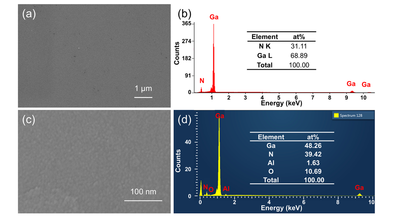
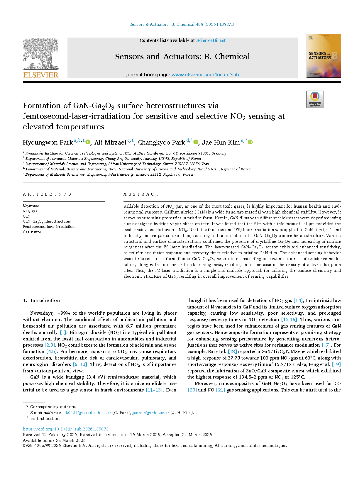
Fig. 1. Top-view SEM images and corresponding SEM–EDS spectra of GaN films with different thicknesses deposited on sapphire substrates: (a,b) ~2 um-thick GaN film and (c,d) ~500 nm-thick GaN film.
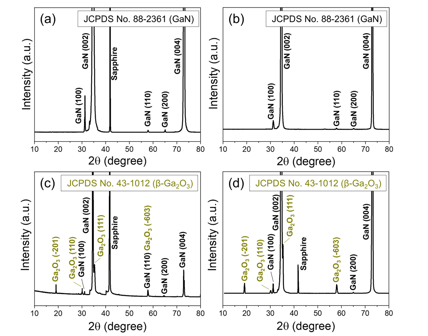
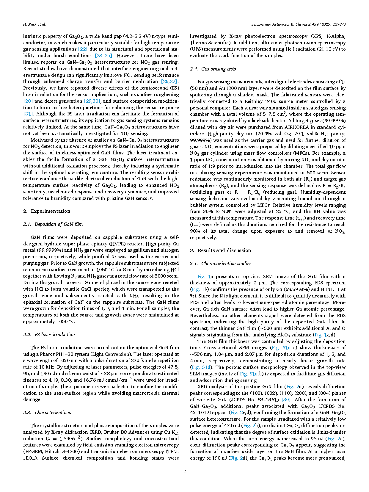
Fig.2. XRD patterns of (a) GaN film and GaN films irradiated with FS laser pulse energies of (b) 47.5 nJ, (c) 95 nJ, and (d) 190 nJ.
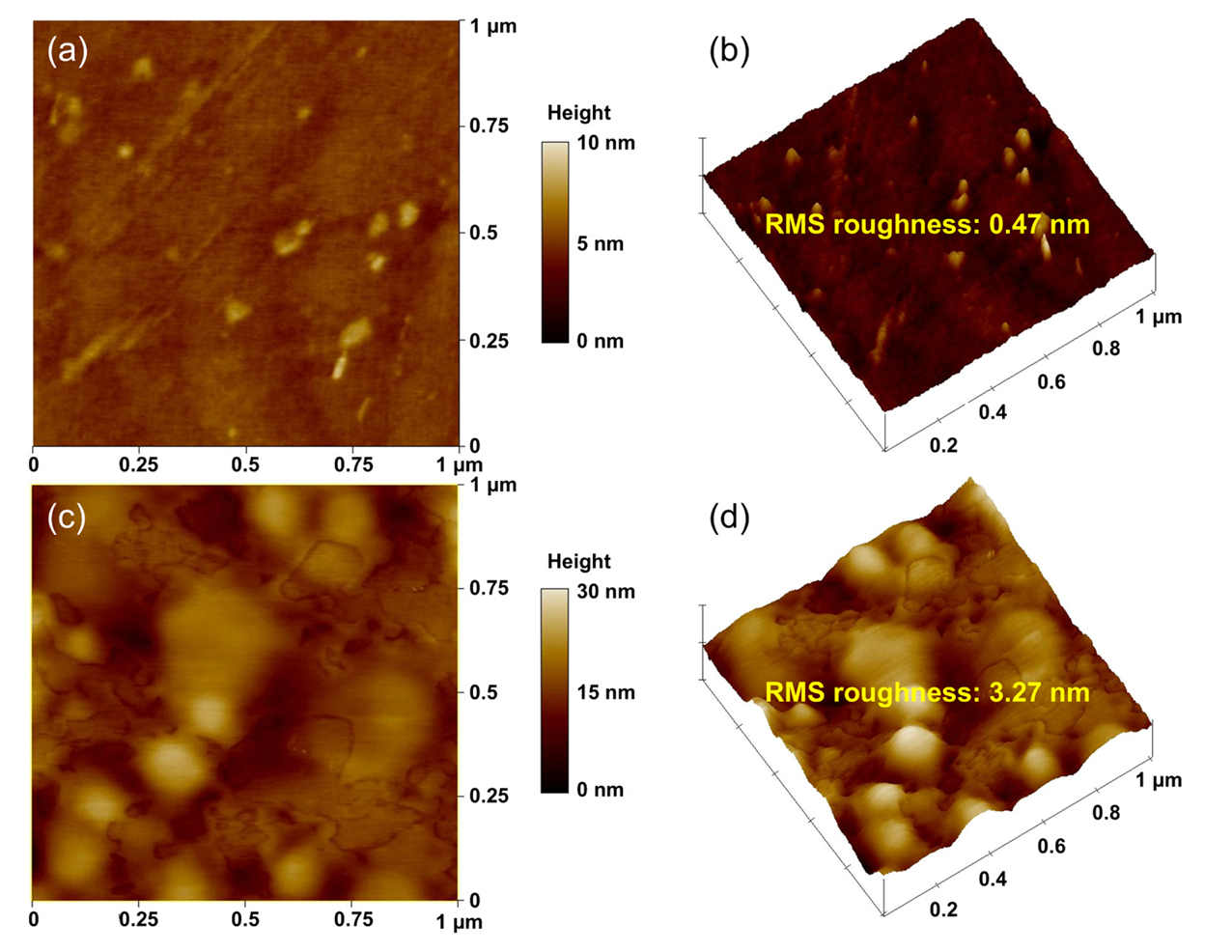
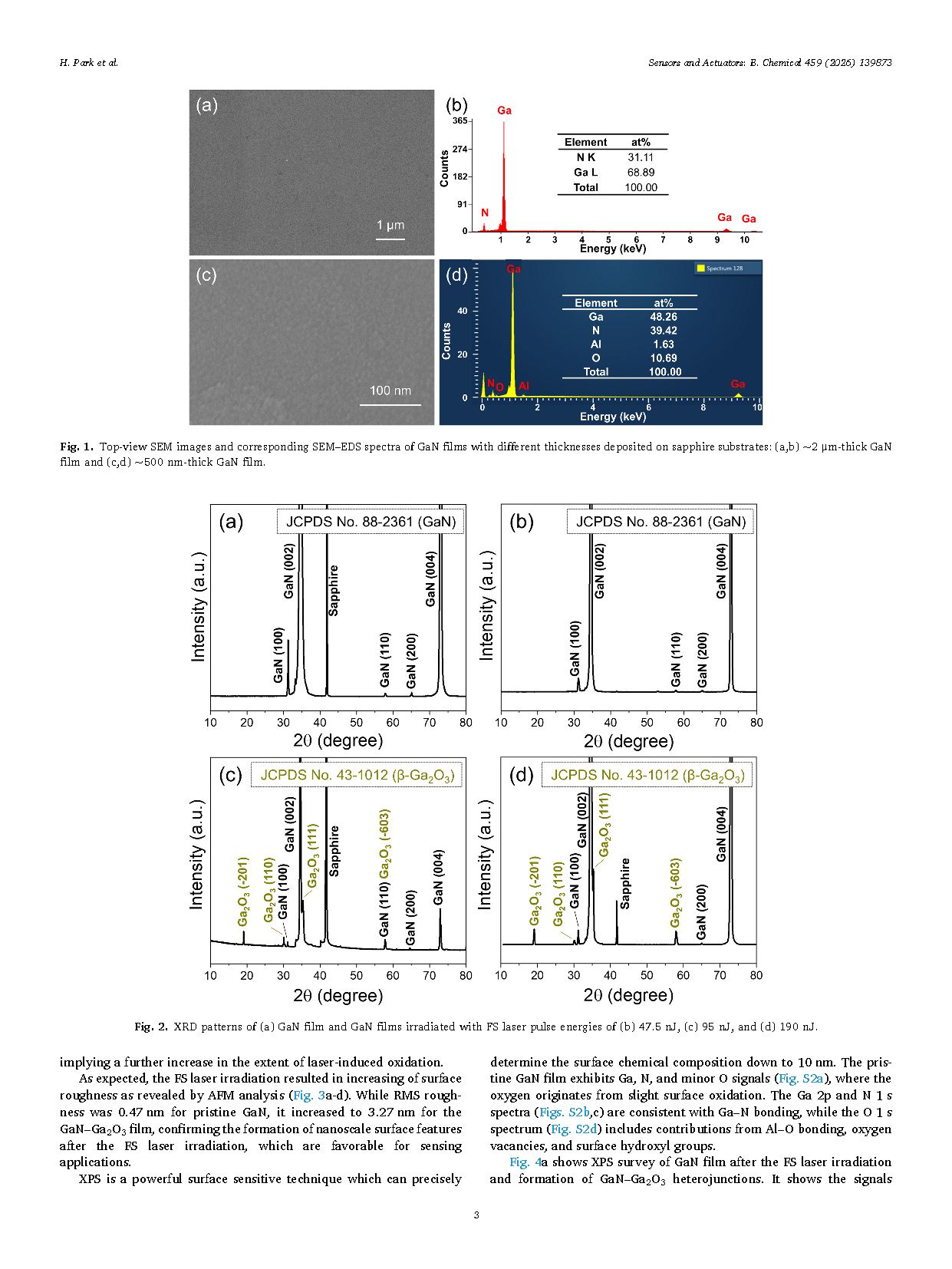
Fig. 3. AFM images of (a)-(b)GaN and (c)-(d)GaN–Ga2O3 films.
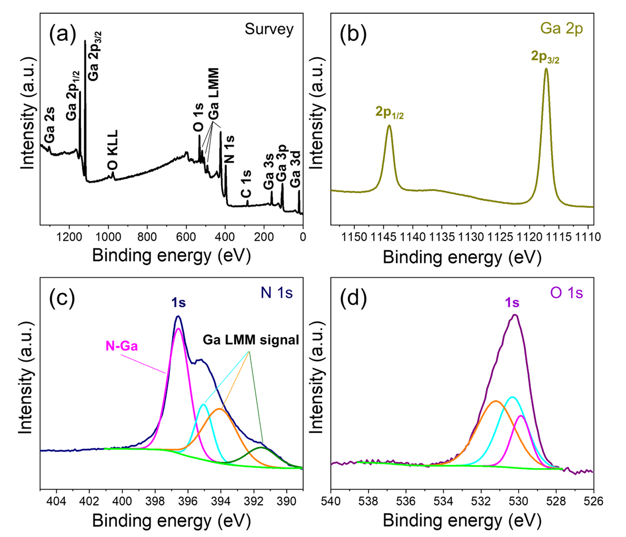
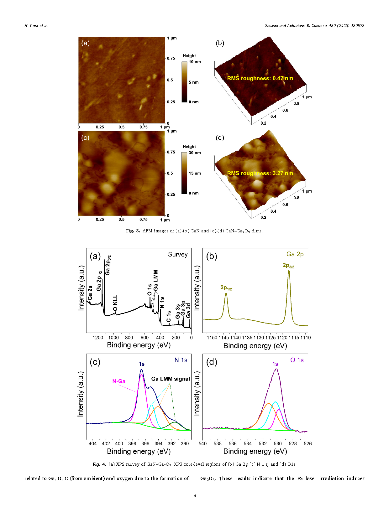
Fig. 4. (a) XPS survey of GaN–Ga2O3. XPS core-level regions of (b) Ga 2p (c) N 1 s, and (d) O 1s.
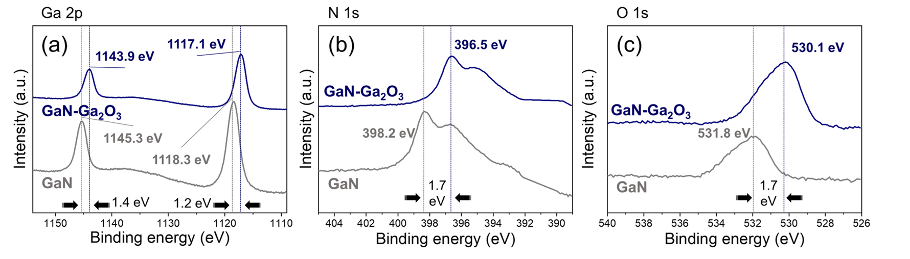
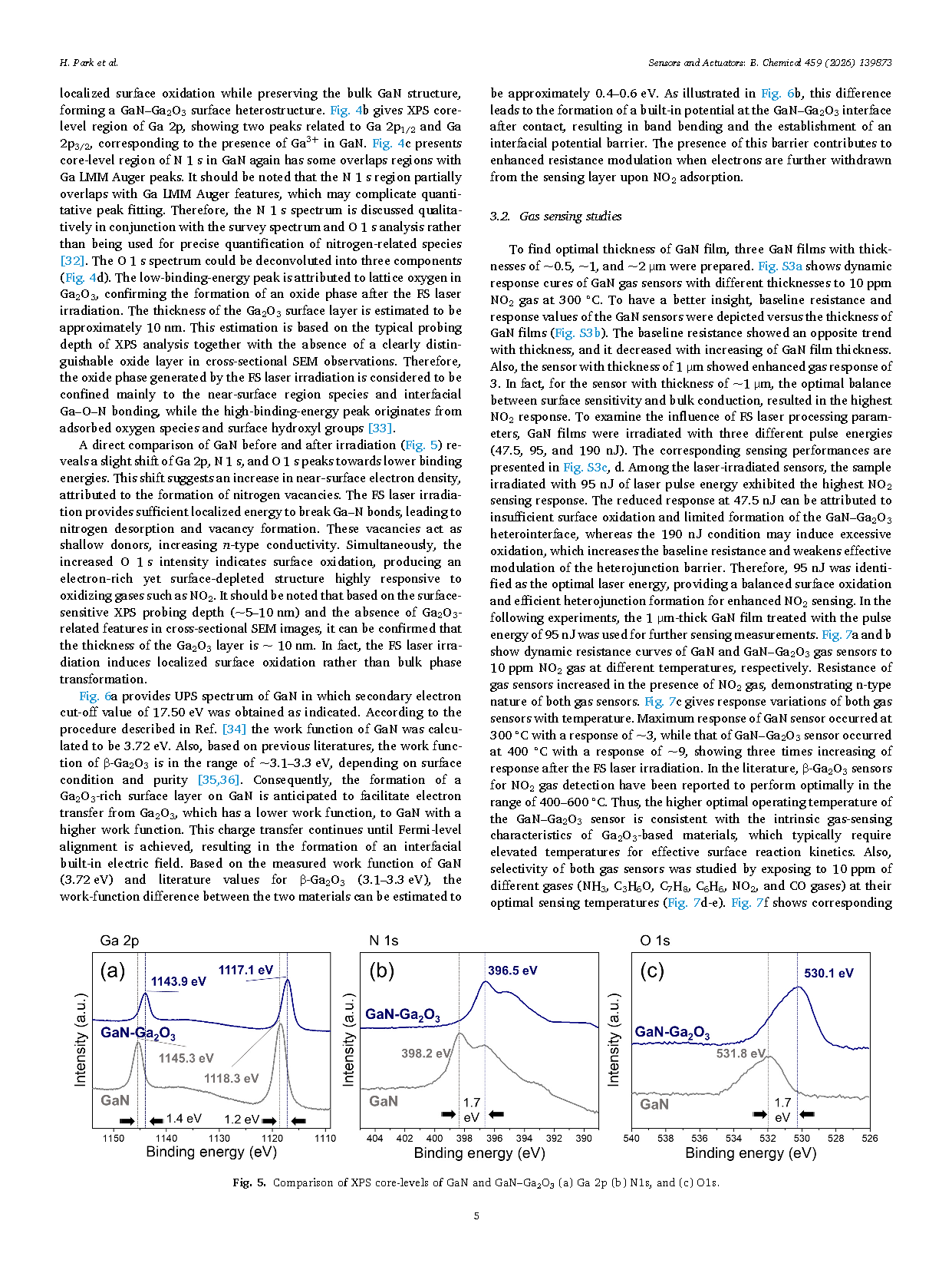
Fig. 5. Comparison of XPS core-levels of GaN and GaN–Ga2O3 (a) Ga 2p (b) N 1s, and (c) O 1s.
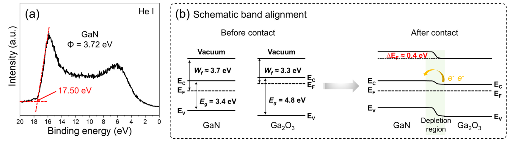
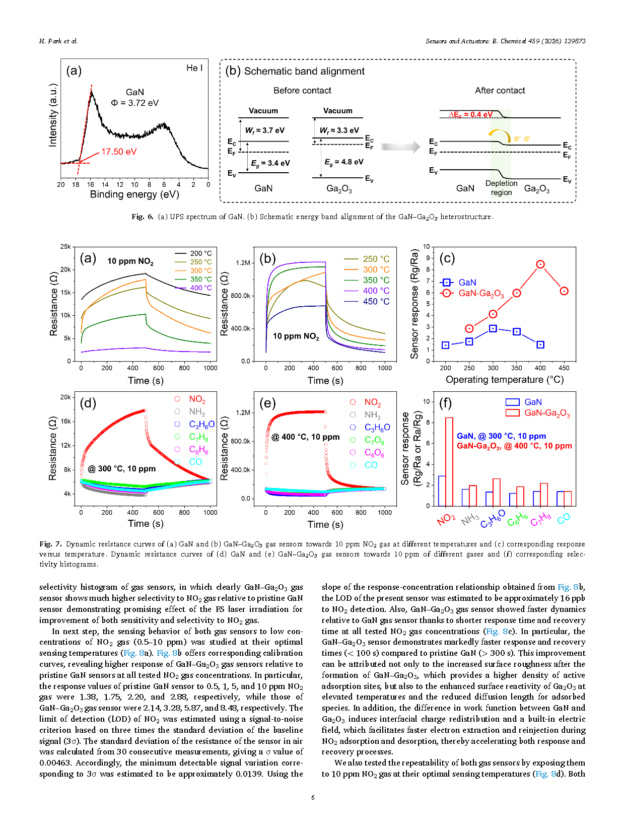
Fig. 6. (a) UPS spectrum of GaN. (b) Schematic energy band alignment of the GaN–Ga2O3 heterostructure.
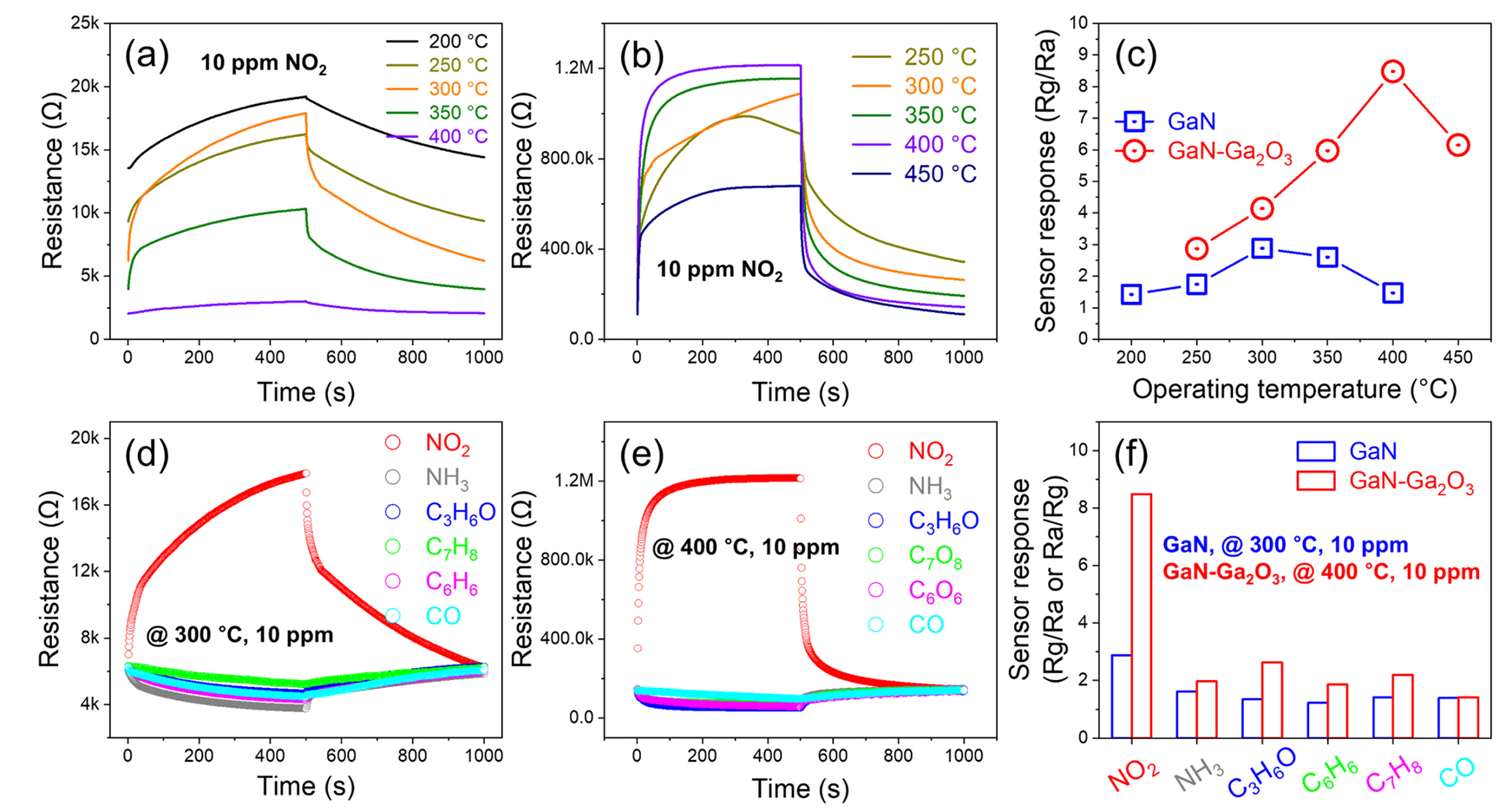
Fig. 7. Dynamic resistance curves of (a) GaN and (b) GaN–Ga2O3 gas sensors towards 10 ppm NO2 gas at different temperatures and (c) corresponding response versus temperature. Dynamic resistance curves of (d) GaN and (e) GaN–Ga2O3 gas sensors towards 10 ppm of different gases and (f) corresponding selectivity histograms.
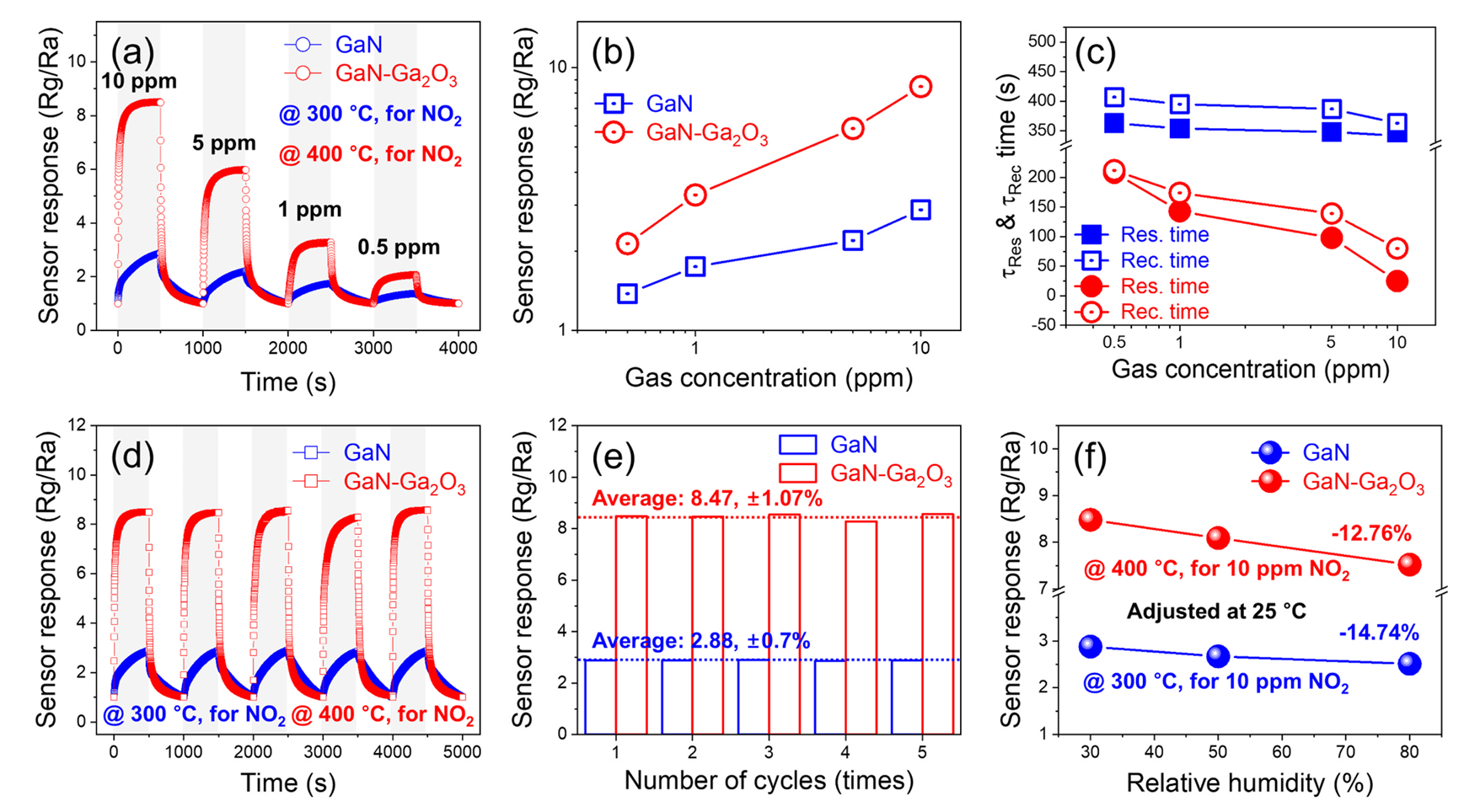
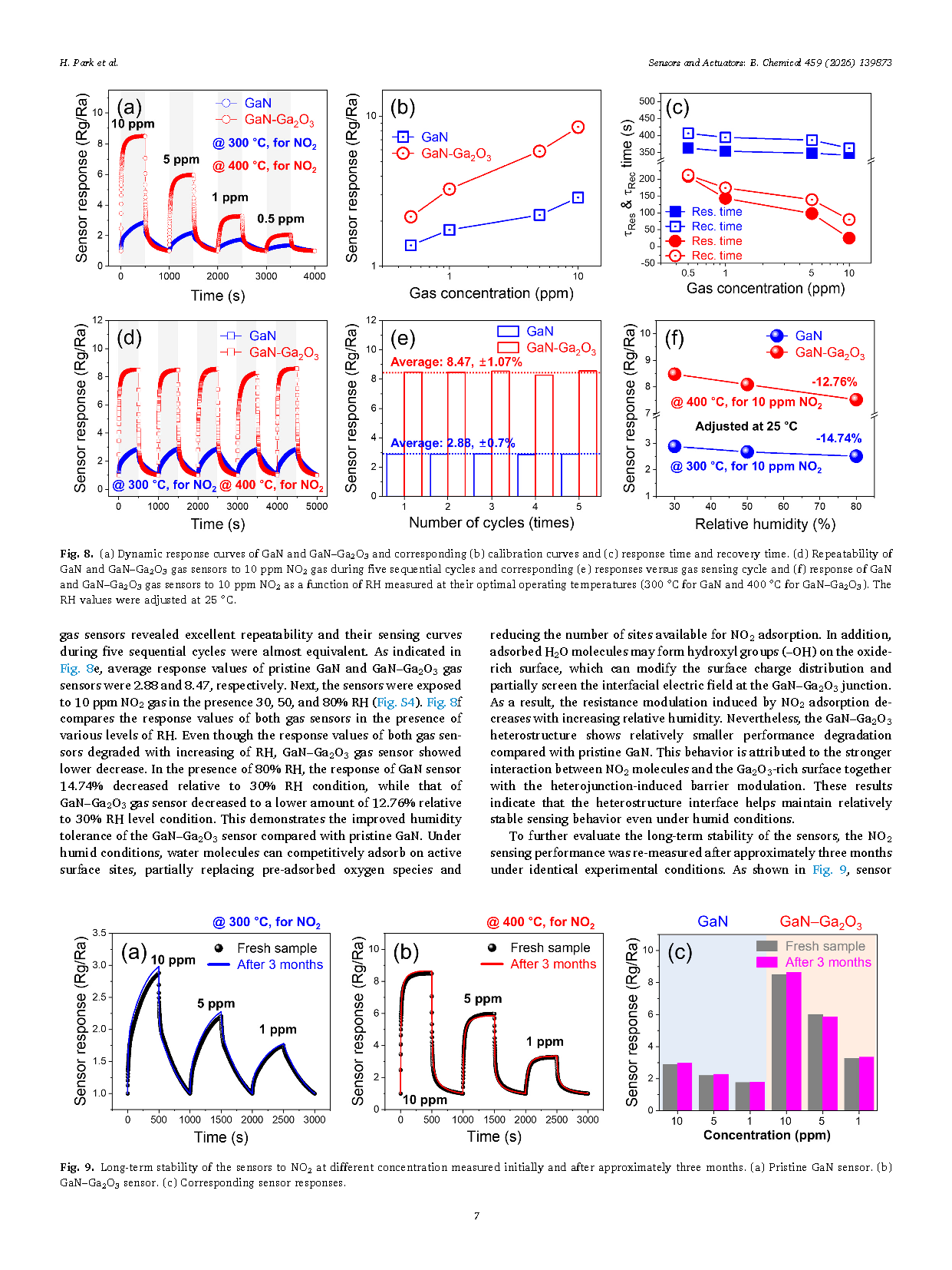
Fig. 8. (a) Dynamic response curves of GaN and GaN–Ga2O3 and corresponding (b) calibration curves and (c) response time and recovery time. (d) Repeatability of GaN and GaN–Ga2O3 gas sensors to 10 ppm NO2 gas during five sequential cycles and corresponding (e) responses versus gas sensing cycle and (f) response of GaN and GaN–Ga2O3 gas sensors to 10 ppm NO2 as a function of RH measured at their optimal operating temperatures (300℃for GaN and 400℃ for GaN–Ga2O3 ). The RH values were adjusted at 25℃.
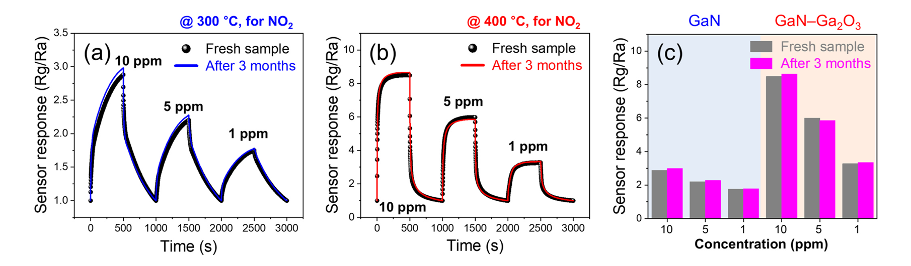
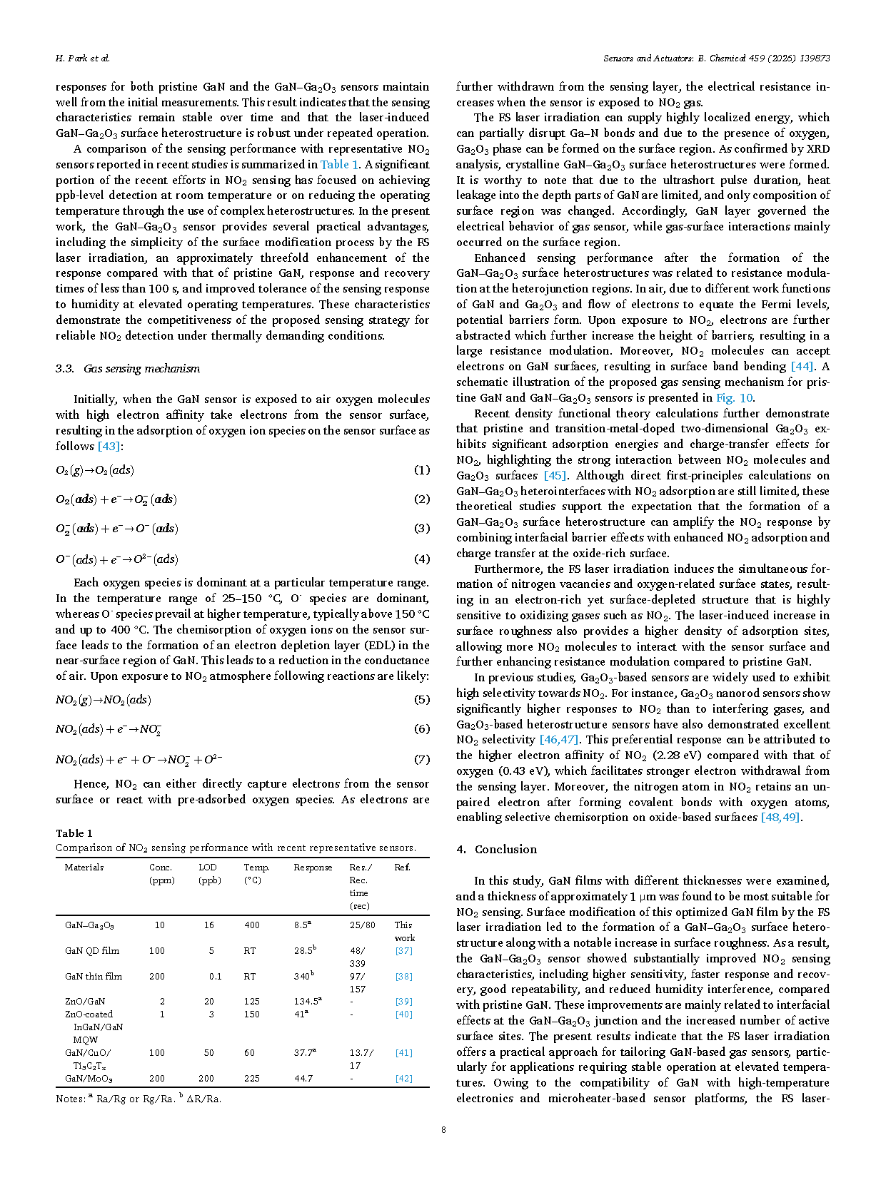
Fig. 9. Long-term stability of the sensors to NO2 at different concentration measured initially and after approximately three months. (a) Pristine GaN sensor. (b) GaN–Ga2O3 sensor. (c) Corresponding sensor responses.
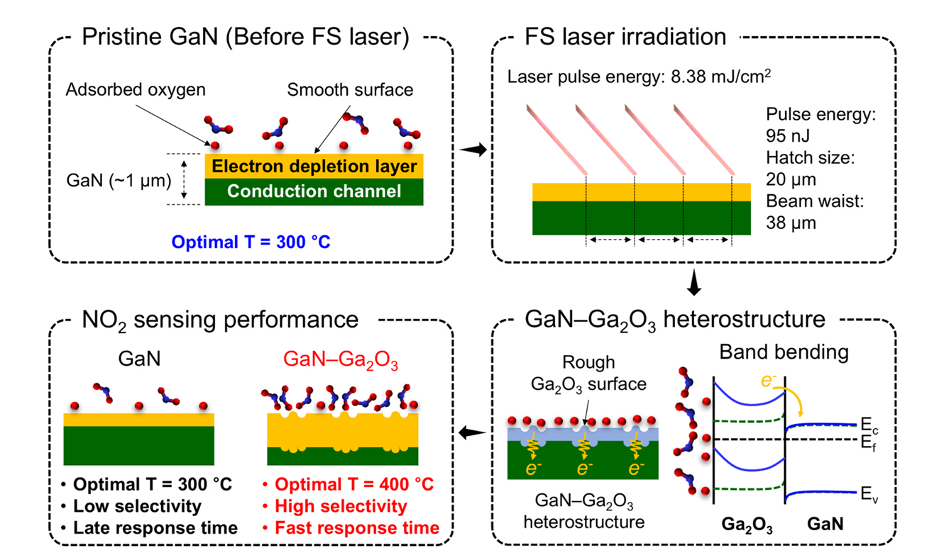
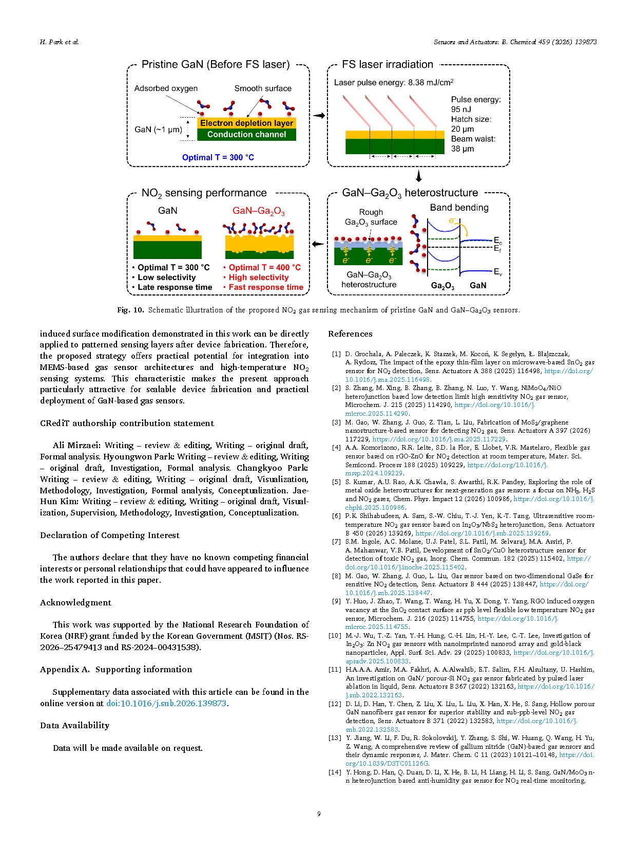
Fig. 10. Schematic illustration of the proposed NO2 gas sensing mechanism of pristine GaN and GaN–Ga2O3 sensors.
DOI:
doi.org/10.1016/j.snb.2026.139873