


News Trends
【Domestic News】Gallium Oxide and Diamond Heterogeneous Integration: A Key Path to Breakthroughs in Thermal Management and P-type Bottlenecks
日期:2026-04-07阅读:401
Gallium oxide is an ultra-wide bandgap semiconductor with a bandgap of approximately 4.9 eV, featuring an extremely high breakdown electric field (~10 MV/cm) and excellent Baliga’s figure of merit, making it highly advantageous for high-voltage power devices. Compared with conventional silicon, its performance potential can be orders of magnitude higher, positioning Gallium Oxide as a key candidate material for devices exceeding 10 kV. Additionally, Gallium Oxide shows promising applications in optoelectronics, such as deep-ultraviolet (DUV) photodetection.
However, Gallium Oxide faces two major challenges. First, its intrinsic thermal conductivity is relatively low (typically <30 W/m·K), leading to significant self-heating under high-power operation, which can degrade or even damage device performance. Second, achieving p-type doping is extremely difficult due to factors such as the stability of oxygen 2p orbitals, large hole effective mass, and self-compensation effects, making high-performance bipolar devices challenging to realize.
In contrast, diamond exhibits a complementary set of advantages. With a bandgap of up to 5.5 eV and the highest known bulk thermal conductivity (>2000 W/m·K), diamond allows exceptionally efficient heat dissipation. It can also achieve stable p-type conduction via boron doping, with hole mobility far exceeding most semiconductors. Although n-type doping remains difficult, diamond’s strengths in thermal management and p-type conduction can compensate for Gallium Oxide’s shortcomings. Consequently, integrating n-type Gallium Oxide with p-type diamond is considered an ideal approach that combines thermal and electrical advantages.
Recently, a research team from the Ningbo Institute of Materials, Chinese Academy of Sciences, and other institutions published a review paper, “Integrations and Applications of Gallium Oxide and Diamond”, systematically summarizing Gallium Oxide/diamond heterointegration technologies and their application progress.
Several Gallium Oxide/diamond integration approaches exist, each with distinct advantages and limitations.
First, transfer and bonding methods mechanically transfer Gallium Oxide thin films onto diamond substrates to achieve integration. This approach preserves the crystalline quality of both materials and avoids lattice mismatch issues, producing interfaces with extremely low roughness. However, challenges remain in large-area fabrication and process uniformity, limiting scalability.
Second, diamond growth on Gallium Oxide can be attempted, but diamond typically grows under high-temperature hydrogen-rich chemical vapor deposition (CVD) conditions, which can reduce Gallium Oxide and damage the interface. Protective buffer layers, such as SiO₂, are often introduced, but they add thermal resistance and reduce heat management efficiency.
Third, Gallium Oxide growth on diamond is considered more promising. Gallium Oxide thin films can be deposited at relatively low temperatures using techniques such as plasma-enhanced chemical vapor deposition (PECVD), pulsed laser deposition (PLD), or atomic layer deposition (ALD), enabling heteroepitaxy without compromising the diamond structure.
Studies show that both β- and ε-phase Gallium Oxide can be grown on diamond, with ε-Gallium Oxide preferred due to smaller lattice mismatch, facilitating high-quality interfaces. Interface engineering—introducing interlayers such as AlN, Al₂O₃, or graphene—can effectively relieve stress and enhance interfacial thermal conductance. Optimized Gallium Oxide/diamond interfaces have demonstrated thermal boundary conductances ranging from tens to hundreds of MW/m²·K, far surpassing conventional semiconductor systems.
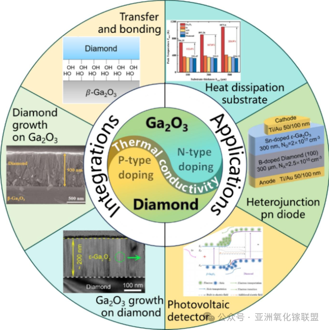
Device applications highlight Gallium Oxide/diamond integration’s value in thermal management. Theory and experiments show that incorporating diamond substrates or heat-spreading layers can reduce Gallium Oxide device peak temperatures by tens to hundreds of degrees Celsius, significantly improving reliability and output power. In high-power MOSFETs, diamond heat paths mitigate current collapse and enhance operational stability. Dual-sided cooling and advanced packaging can further increase device power density.
Moreover, n-type Gallium Oxide/p-type diamond heterojunction devices offer a solution to Gallium Oxide’s p-type doping limitation. These heterojunctions exhibit typical rectifying behavior, with rectification ratios exceeding 10⁷ and breakdown voltages reaching kilovolt levels, in some cases over 3 kV. Both materials’ wide bandgaps ensure stable operation at elevated temperatures, showing potential for high-voltage power electronics.
In optoelectronics, the bandgap difference between Gallium Oxide and diamond provides unique spectral response characteristics. Gallium Oxide responds primarily to 240–260 nm, while diamond covers shorter deep-UV wavelengths. Heterostructures can thus realize broadband DUV photodetectors spanning 210–260 nm, covering the solar-blind region, with applications in space exploration, flame monitoring, and more. Experiments indicate high photo-to-dark ratios and good temperature stability, outperforming single-material devices.
Despite these promising prospects, several challenges remain. Significant differences in thermal expansion and lattice constants can induce interfacial stress and defects. Process environment disparities complicate direct integration, and epitaxial films often fall short of bulk material performance—e.g., polycrystalline diamond exhibits lower thermal conductivity, and interface defects affect electrical behavior. These issues require advanced interface engineering, stress management, and novel process technologies.
Overall, Gallium Oxide/diamond integration represents a major direction in ultra-wide bandgap semiconductors. Their complementary thermal and electrical properties hold promise for breakthroughs in high-voltage power electronics, deep-UV photodetection, and emerging energy devices. With continued advancements in material growth and integration technologies, this “ultimate combination” is poised to drive next-generation high-performance semiconductor devices to new heights.
