


Member News
【Member News】Fujia Gallium Leads China’s Gallium Oxide Industry: Full-Chain Innovation from Material Breakthroughs to Device Performance Limits
日期:2026-04-09阅读:466
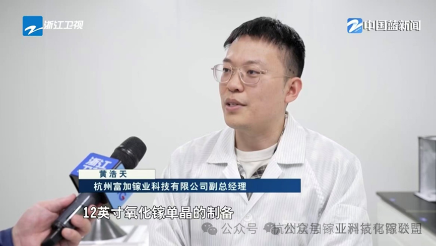
On April 2, 2026, Zhejiang Satellite TV featured an in-depth report titled “The Only One in Zhejiang! Why Scientists Favor This Incubator for Entrepreneurship”, highlighting the technology incubation achievements of the Hangzhou Institute of Optics and Fine Mechanics. Among the cases presented, Hangzhou Fujia Gallium Technology Co., Ltd. was featured as a representative example due to its series of breakthroughs in Gallium Oxide industrialization.
Huang Haotian, Deputy General Manager of the company, stated, “We have successfully fabricated the world’s first 12-inch Gallium Oxide single crystal. This is not merely a change in size—it represents a qualitative leap in industrialization.” For Fujia Gallium, this milestone is not the starting point but a key phase, reflecting a continuous path of industrial advancement.
From Stable Growth to Size Scaling: Advancing toward Industrialization
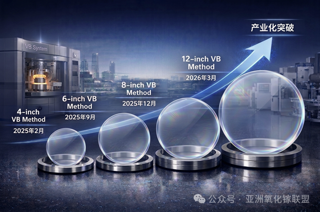
In early 2025, Fujia Gallium successfully achieved stable growth of 4-inch Gallium Oxide single crystals using the VB method and simultaneously launched its proprietary growth equipment and process system, ensuring reproducible crystal growth. The company then continuously pushed the limits of crystal size: in September 2025, it produced 6-inch VB single crystals for the first time; in December, in collaboration with the Shanghai Institute of Optics and Fine Mechanics, Chinese Academy of Sciences, it achieved 8-inch crystal growth; by March 2026, Fujia Gallium successfully fabricated the world’s first 12-inch Gallium Oxide single crystal.
Scaling from 4 inches to 12 inches was not merely a matter of enlarging size—it represented a rigorous test of engineering capabilities across every step, including equipment fabrication, thermal field design, crystal growth stability, and stress management. This milestone marks a critical transition of Gallium Oxide material from laboratory samples to industrial-scale manufacturing.
From Material Capability to Challenging Device Performance Limits
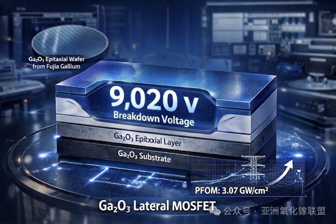
Merely scaling up size and improving fabrication capabilities keeps industrialization at the “possibility” stage. The true measure of technological value lies in device-level performance. On March 31, 2026, Jiufengshan Laboratory announced that its Gallium Oxide lateral MOSFET achieved a breakdown voltage exceeding 9,000 V (measured at 9.02 kV). Against an industry backdrop where typical performance remains below 4,000 V, this represents a significant leap.
The key material used in this device—a domestically produced homoepitaxial wafer—was supplied by Fujia Gallium. This result highlights more than just a single device performance improvement; it reveals a fundamental truth: Chinese materials are defining the upper limits of device performance. Previously, vertical power Schottky diodes fabricated using Fujia Gallium epitaxial wafers achieved a power figure-of-merit (PFOM) of 3.07 GW/cm², ranking among the highest publicly reported levels internationally. Continuous device validation has transformed material capabilities from mere parameter metrics into tangible device performance boundaries.
From “Single-Point Breakthroughs” to “Full-Chain Collaboration”
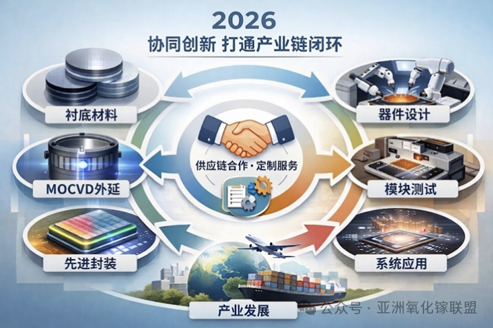
With continuous advances in material and device performance, Fujia Gallium has gradually built a vertically integrated capability covering the full chain from substrates to epitaxy and device validation. In 2025, the company achieved multiple advances in areas such as MOCVD homoepitaxy, high-mobility material fabrication, and device prototyping. At the same time, by launching multi-crystal-plane substrate products, offering customized services, and establishing strategic partnerships with international companies, it steadily connected the upstream and downstream of the industry chain.
At this stage, the key is no longer breakthroughs at a single technical point, but whether effective collaboration and closed-loop integration can be established across different stages of the chain.
Conclusion
The Zhejiang TV report reveals more than a single technological achievement; it reflects a progressively maturing industrialization pathway:
●From crystal growth to size scaling
●From material capability to device validation
●From single-point breakthroughs to full-chain collaboration
This innovative trajectory has not only advanced Gallium Oxide from a laboratory-emerging material to large-scale application, but also underscores the strength of China’s semiconductor materials industry. As a council member of the Asian Gallium Oxide Alliance, Fujia Gallium, with the mission of “bringing high-quality materials to the world,” continuously promotes the stability and yield of Gallium Oxide single crystals, accelerating the pace of industrialization and securing a leading position in the industry.
Throughout this process, the Alliance has provided strategic support to Fujia Gallium, helping drive upstream and downstream collaboration, and continuously optimizing the Gallium Oxide industrial ecosystem. From material breakthroughs to pushing the limits of device performance, China’s Gallium Oxide industry is evolving from a “participant” to a “definer,” with Fujia Gallium at the forefront, leading global Gallium Oxide technology development with innovation and strength, and writing a new chapter in China’s wide-bandgap semiconductor materials landscape.
