


News Trends
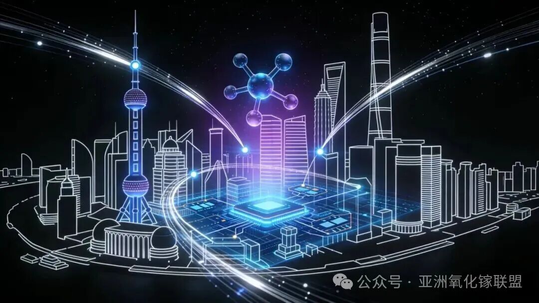
【Domestic News】Shanghai "Goes All In" on Fourth-Generation Semiconductors: Gallium Oxide Emerging as the Core Variable
日期:2026-04-13阅读:656
On February 3, at the opening of the Fourth Session of the 16th Shanghai Municipal People's Congress held at the Expo Center, Shanghai Mayor Gong Zheng delivered the Government Work Report. The report explicitly proposed that Shanghai will advance the construction of the Lin-gang Science and Technology City this year, accelerate the creation of high-level sci-tech communities, and continuously enhance the energy levels of specialized industrial parks such as the Oriental Chip Port and the Aviation Industrial Park. Furthermore, the city will vigorously cultivate and develop future industries, including brain-computer interfaces and fourth-generation semiconductors.
As a "global economic hub," Shanghai's clear commitment to "going long" on fourth-generation semiconductors is set to drive a new technological revolution. As issues like low phone battery anxiety and high energy consumption in data centers become increasingly prominent, and while range anxiety for New Energy Vehicles (NEVs) persists, fourth-generation semiconductors are breaking through the ice, armed with the brilliance of Gallium Oxide, the chill of diamond, and the resilience of aluminum nitride.
What are the Application Scenarios for Fourth-Generation Semiconductors?
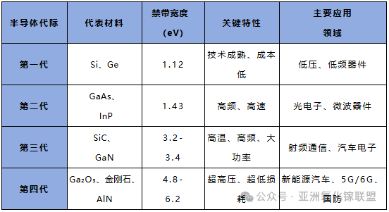
Starting from silicon-based materials, the semiconductor system has completed four rounds of technological evolution and is now entering the fourth-generation phase, characterized by ultra-wide bandgap (UWBG) materials. This stage is represented by Gallium Oxide (Gallium Oxide), Diamond, and Aluminum Nitride (AlN), with bandgaps typically exceeding 4.8 eV, significantly breaking the physical limits of traditional silicon.
Compared to previous material systems, ultra-wide bandgap semiconductors offer advantages in three key performance metrics: wider bandgap, higher critical breakdown electric field, and superior thermal conductivity. Taking Gallium Oxide as an example, its bandgap is approximately 4.9 eV, and its breakdown field strength can reach 8 MV/cm—more than 20 times that of silicon. In terms of theoretical power loss, it is only about 1/3000 of silicon and 1/6 of silicon carbide.
Based on these characteristics, these materials demonstrate higher stability and efficiency under extreme conditions such as high temperatures, high frequencies, and high voltages, providing significant performance headroom for power electronics and RF communications.
Key High-End Application Scenarios:
Scenario 1: NEVs and Ultra-High Voltage Charging
Gallium Oxide devices can significantly reduce the volume and increase the efficiency of on-board chargers (OBC) and inverters, serving as a key enabler for the popularization of 800V and higher voltage platforms.
Scenario 2: Power Systems
Applications in UHVDC (Ultra-High Voltage Direct Current) transmission, photovoltaic inverters, and smart grid circuit breakers can drastically reduce energy transmission losses.
Scenario 3: High-End Equipment and National Defense
Their high-temperature and radiation-resistant properties are ideal for power systems in aerospace vehicles. Diamond also shows potential in microwave weapons and quantum sensors.
Scenario 4: Frontier Tech and Thermal Management
The extremely high thermal conductivity of diamond is the ideal solution for the heat dissipation bottlenecks in high-power density devices like AI chips. Aluminum Nitride is a critical material for deep ultraviolet (DUV) photodetectors.
The 5-Layer "Mapping" of the Industrial Chain
This analysis focuses on the fourth-generation semiconductor industrial system, organized into five levels: Materials — Substrates/Epitaxy — Device Manufacturing — Packaging & Testing/Equipment — Applications.
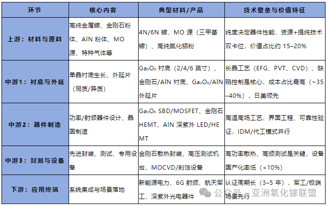
Upstream: Materials and Raw Materials
The chain starts with high-purity raw materials and precursors. Gallium metal is extracted via the Bayer process (purities up to 4N+), then converted into MO sources (Trimethylgallium) to prepare Gallium Oxide polycrystalline material. China accounts for approximately 70% of global gallium resources, but still relies on imports for high-purity refining and critical equipment.
Midstream (I): Substrates and Epitaxy (The Core Value Link)
Gallium Oxide Substrates: Mainstream processes include EFG (Edge-defined Film-fed Growth) and VB (Vertical Bridgman). Japan's NCT has achieved 6-inch mass production. China has made breakthroughs in 4-6 inch substrates, though yield rates (approx. 30%) still trail Japan (approx. 60%).
Diamond Substrates: Primarily rely on CVD (Chemical Vapor Deposition) heteroepitaxy. The difficulty lies in large-size uniformity and defect control.
Aluminum Nitride Substrates: Grown using the PVT (Physical Vapor Transport) method. Seed crystal resources are highly dependent on Japanese manufacturers.
Midstream (II): Device Manufacturing (Design and Process)
Power Devices (Gallium Oxide-based): Includes Schottky Barrier Diodes (SBD) and MOSFETs. Suitable for 1.2–3.3 kV voltage levels.
RF Devices (AlN/Diamond-based): Covers HEMT and terahertz devices for 6G and radar applications, with operating frequencies exceeding 100 GHz.
Optoelectronic Devices (AlN-based): Focused on UVC LEDs and DUV detection (200–280 nm).
Midstream (III): Packaging, Testing, and Equipment
Packaging: High-power packaging focuses on using diamond heat-spreading substrates and double-sided cooling to compensate for the low thermal conductivity of Gallium Oxide.
Equipment: Includes growth furnaces (EFG, PVT, CVD). Front-end equipment like MOCVD, etching, and ion implantation is still dominated by firms like Applied Materials and TEL.
Downstream: Application Terminals
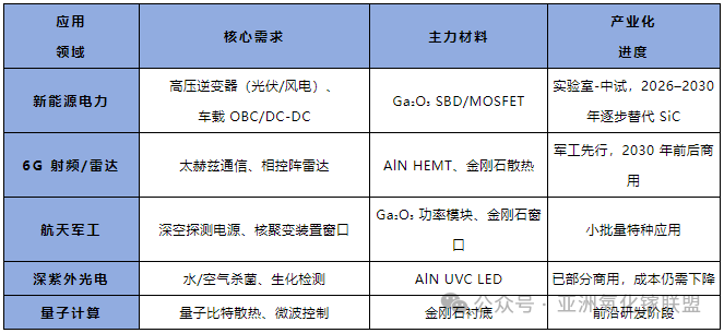
Characteristics: Military and aerospace sectors lead with early verification. New energy power systems represent the largest potential market, pending cost reductions and reliability data accumulation.
The "Hidden Champions" Corporate List
As of late 2025, the representative players include:
Overseas: NCT (Gallium Oxide), Element Six (Diamond), and Kyma (AlN) are material leaders.
Domestic (China): A chain consisting of Garen Semiconductor/Fujia Gallium — San'an Optoelectronics/CETC — JCET/Naura has formed, though most are in the pilot-to-small-batch production stage.
A New Global Battlefield for Tech Innovation?
The global landscape shows a "Bipolar Dominance, Multi-point Breakthrough" pattern:
Japan: Dominates Gallium Oxide with 68% of related patents.
United States: Focuses on high-end and military applications via DARPA projects, and occupies 90% of the AlN RF device market. The U.S. has also placed Gallium Oxide substrates on export control lists.
China: Shows strong momentum. Hangzhou Garen Semiconductor released the world's first 8-inch Gallium Oxide single crystal, while CETC 46th Institute successfully prepared the first domestic 6-inch Gallium Oxide single crystal.
European Union: Focuses on joint investments and automotive-grade applications, with plans to invest €2.2 billion in an 8-inch diamond pilot line.
Outlook: While challenges like P-type doping in Gallium Oxide and the high cost of large-scale diamond crystals remain, the next 3-5 years will see the scale-up of 6-inch and 8-inch production lines. Fourth-generation semiconductors are expected to begin partially replacing third-generation semiconductors in key sectors like new energy.
