Paper Sharing
【Member Papers】Laser-assisted in situ fabrication of atomically thin Ga₂O₃ films for dielectric applications
日期:2026-04-17阅读:74
Researchers from the Nanjing Tech University and Southern University of Science and Technology have published a dissertation titled " Laser-assisted in situ fabrication of atomically thin Ga2O3 films for dielectric applications" in FlexMat.
Background
Two‐dimensional (2D) gallium oxide (Ga₂O₃) has emerged as a high‐κ dielectric material for optoelectronic applications due to its ultra‐wide bandgap and large‐scale productivity. However, the usage of thermal treatment during the liquid‐metal‐assisted fabrication process could degrade the quality of channel materials. Conventional fabrication methods for 2D Ga₂O₃, such as solution‐based synthesis, chemical vapor deposition (CVD), and physical vapor deposition (PVD), face significant challenges. Solution‐based approaches require high‐temperature annealing, vapor deposition techniques rely on hazardous chemical precursors or vacuum processing, and liquid metal‐based techniques still necessitate a thermal annealing process, introducing imperfections in oxygen‐sensitive materials.
Abstract
Two‐dimensional (2D) gallium oxide (Ga₂O₃) has emerged as a high‐κ dielectric material for optoelectronic applications due to its ultra‐wide bandgap and large‐scale productivity. However, the usage of thermal treatment during the liquid‐metal‐assisted fabrication process could degrade the quality of channel materials. Here, we report a laser‐assisted in situ oxidation method combined with a confinement template‐assisted squeeze technique to fabricate centimeter‐scale 2D atomically thin Ga₂O₃ films from liquid gallium metal surfaces at room temperature. This approach avoids thermal damage to vulnerable materials. The laser‐accelerated oxidation mechanism is elucidated as photocatalytic oxidation of initial Ga/Ga₂O₃₋ₓ surface through the integration of multi‐wavelength laser radiation experiments and density functional theory calculations. We further demonstrate top‐gated field‐effect transistors (FETs) using black phosphorus (BP) and MoS₂ as channel materials, with thin‐film Ga₂O₃ as the gate dielectrics. BP‐based FETs show gate‐ tunable mid‐infrared photoresponse with responsivity at the order of 0.1 A·W⁻¹ level. MoS₂‐based FETs exhibit a photo‐detectivity of 6.8 ×10¹² Jones in the visible‐light spectrum, an on/off ratio over 10⁸, a subthreshold swing of 73.6 mV decade⁻¹, and gate leakage currents below 4 ×10⁻⁶ A cm⁻² at 8 MV cm⁻¹. This room‐temperature laser‐oxidation approach enables scalable integration of ultrathin oxide dielectrics with sensitive 2D materials for next‐generation nanoelectronics.
Highlights
A laser-assisted in situ oxidation method combined with a confinement template-assisted squeeze technique is developed to fabricate centimeter-scale atomically thin Ga₂O₃ films at room temperature, avoiding thermal damage to thermally vulnerable 2D materials.
The laser-accelerated oxidation mechanism is elucidated as the photocatalytic oxidation of the non-stoichiometric Ga/Ga₂O₃₋ₓ surface, with shorter-wavelength laser irradiation showing higher oxidation efficiency.
The as-prepared Ga₂O₃ films serve as high-performance gate dielectrics and encapsulation layers for air-sensitive 2D materials like black phosphorus (BP).
Top-gated MoS₂ FETs with the Ga₂O₃ dielectric exhibit an on/off ratio over 10⁸, a subthreshold swing of 73.6 mV decade⁻¹, a detectivity up to 6.8 ×10¹² Jones, and ultralow gate leakage currents below 4 ×10⁻⁶ A cm⁻² at 8 MV cm⁻¹.
Conclusion
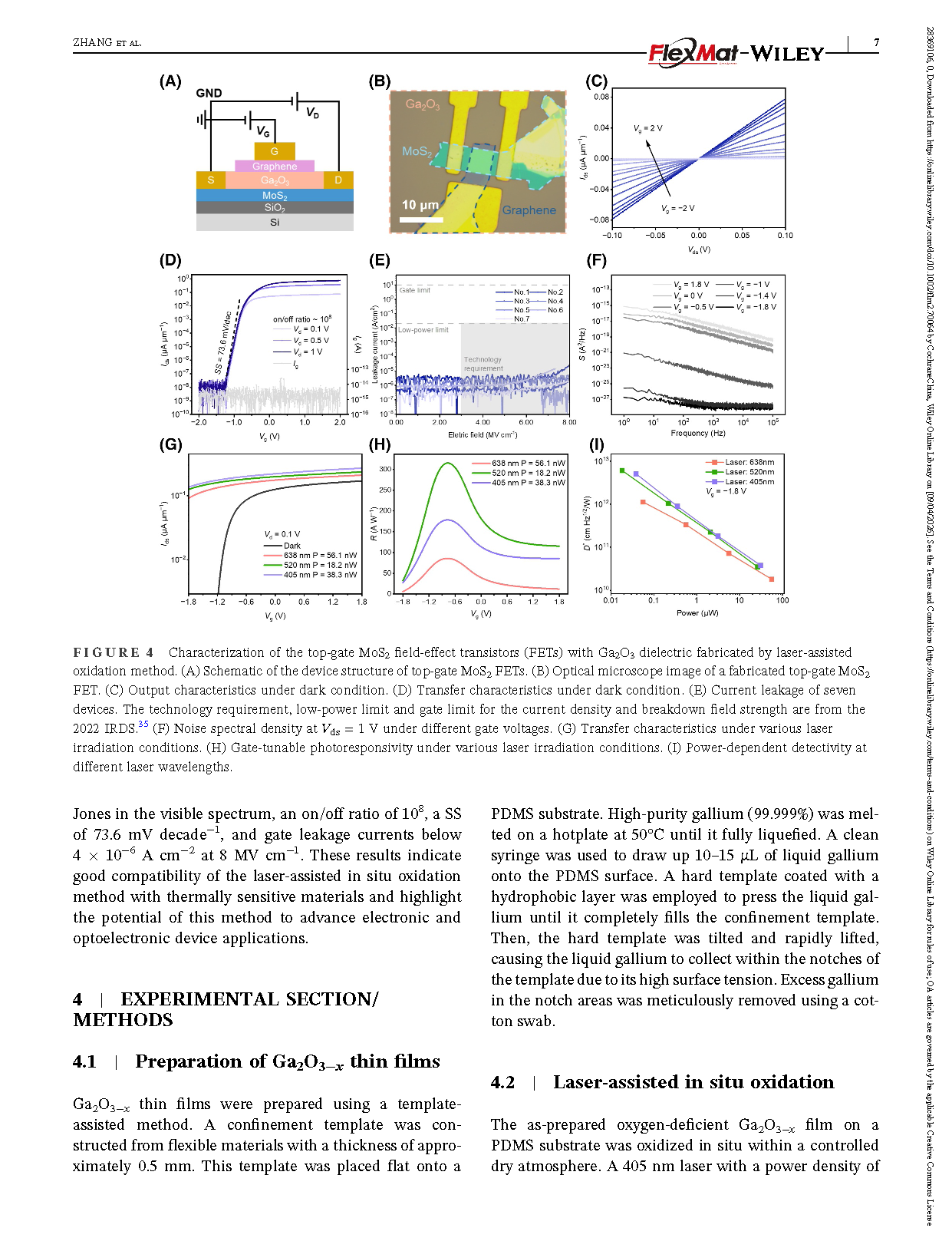
This study presents a laser‐assisted in situ oxidation method, combined with a confinement template‐assisted squeeze technique, to fabricate atomically thin Ga₂O₃ films for dielectric applications. This approach addresses the limitations of conventional thermal annealing, which can cause thermal damage to sensitive materials, enabling the production of centimeter‐scale and high‐quality Ga₂O₃ films. The changes in optical contrast and electrical resistance upon laser irradiation demonstrate that laser irradiation significantly accelerates the oxidation process. The first‐principles calculations reveal the critical role of laser‐induced non‐equilibrium free carriers in enhancing oxidation kinetics. The resulting Ga₂O₃ films were successfully employed as dielectric layers in phototransistors with BP and MoS₂ as channel materials. BP‐based phototransistors exhibit gate‐tunable photoresponse in the mid‐infrared range with a room‐temperature responsivity at order of 0.1 A·W⁻¹ level. MoS₂‐based FETs demonstrate a detectivity of 6.8 ×10¹² Jones in the visible spectrum, an on/off ratio of 10⁸, a SS of 73.6 mV decade⁻¹, and gate leakage currents below 4 ×10⁻⁶ A cm⁻² at 8 MV cm⁻¹. These results indicate good compatibility of the laser‐assisted in situ oxidation method with thermally sensitive materials and highlight the potential of this method to advance electronic and optoelectronic device applications.
Project Support
National Natural Science Foundation of China, Grant/Award Numbers: 62275117, 62374079, 62304097, 92477123, 52373290, 62288102, U25A20484; Shenzhen Excellent Youth Program, Grant/Award Number: RCYX20221008092900001; The Pearl River Talent Recruitment Program, Grant/Award Number: 2019QN01C177; Guangdong Basic and Applied Basic Research Foundation, Grant/Award Number: 2024A1515030224; Shenzhen Fundamental Research Program, Grant/Award Number: JCYJ20240813094508011
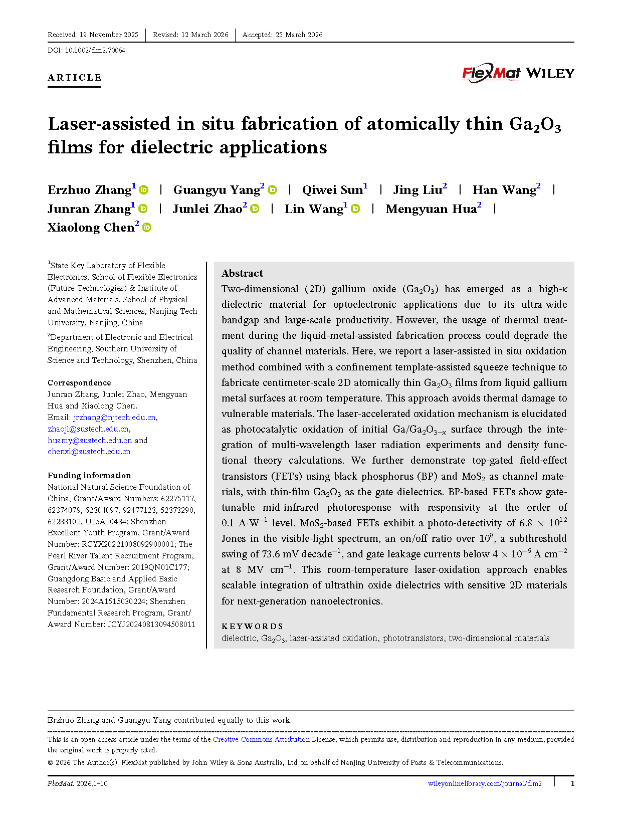
Figure 1 Fabrication and characterization of thin‐film Ga₂O₃ using laser‐assisted in situ oxidation method. (A) Schematic flow of template-assisted preparation of Ga2O3 films. (B) Optical microscope images of as-prepared Ga2O3-x films made on PDMS. (C) Optical microscope image showing the laser irradiation area of thin-film Ga2O3 on the SiO2/Si wafer. (D) Time-dependent resistance change ratio of Ga2O3−x film under laser irradiation with various laser wavelengths. (E) Net oxidation rate at different laser wavelengths.
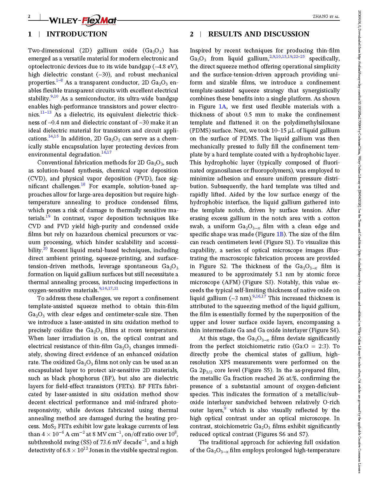
Figure 2 Electronic structure and atomic configurations of thin‐film Ga and Ga2O3-x. (A–D) The density of states (DOS) and atomic configurations of thin-film (A) Ga (B) GaO0.3 (C) GaO and (D) Ga2O3. (B–C) The supercell structure and the corresponding real-space probability distribution of (B) thin-film GaO0.3 of the electronic band from −4 to 0 eV (C) thin-film GaO of the upper tail of the valence band (at Γ k-point), with the isosurface level at 6.37×10⁻². (E–F) Comparison of the coordination environments of (E) Ga and (F) O in thin film GaO0.3, GaO and Ga2O3 with a cutoff distance of 2.4 Å.
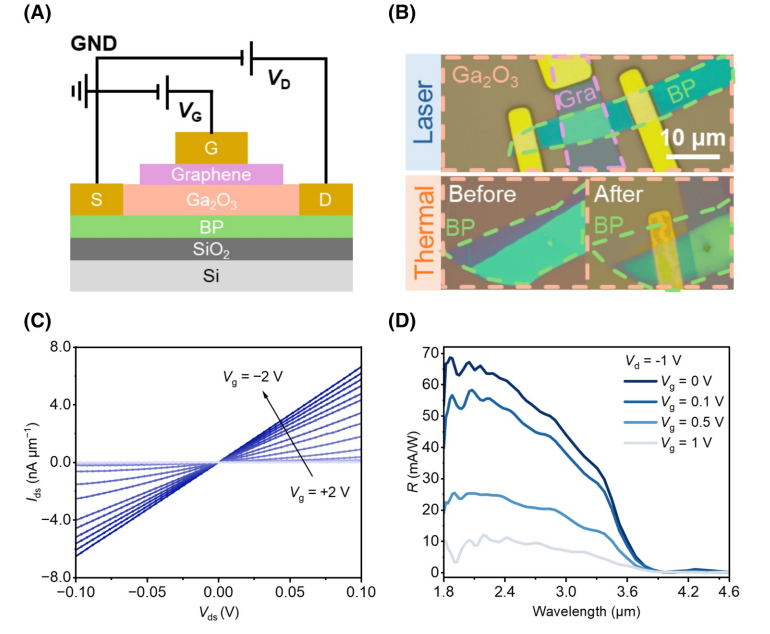
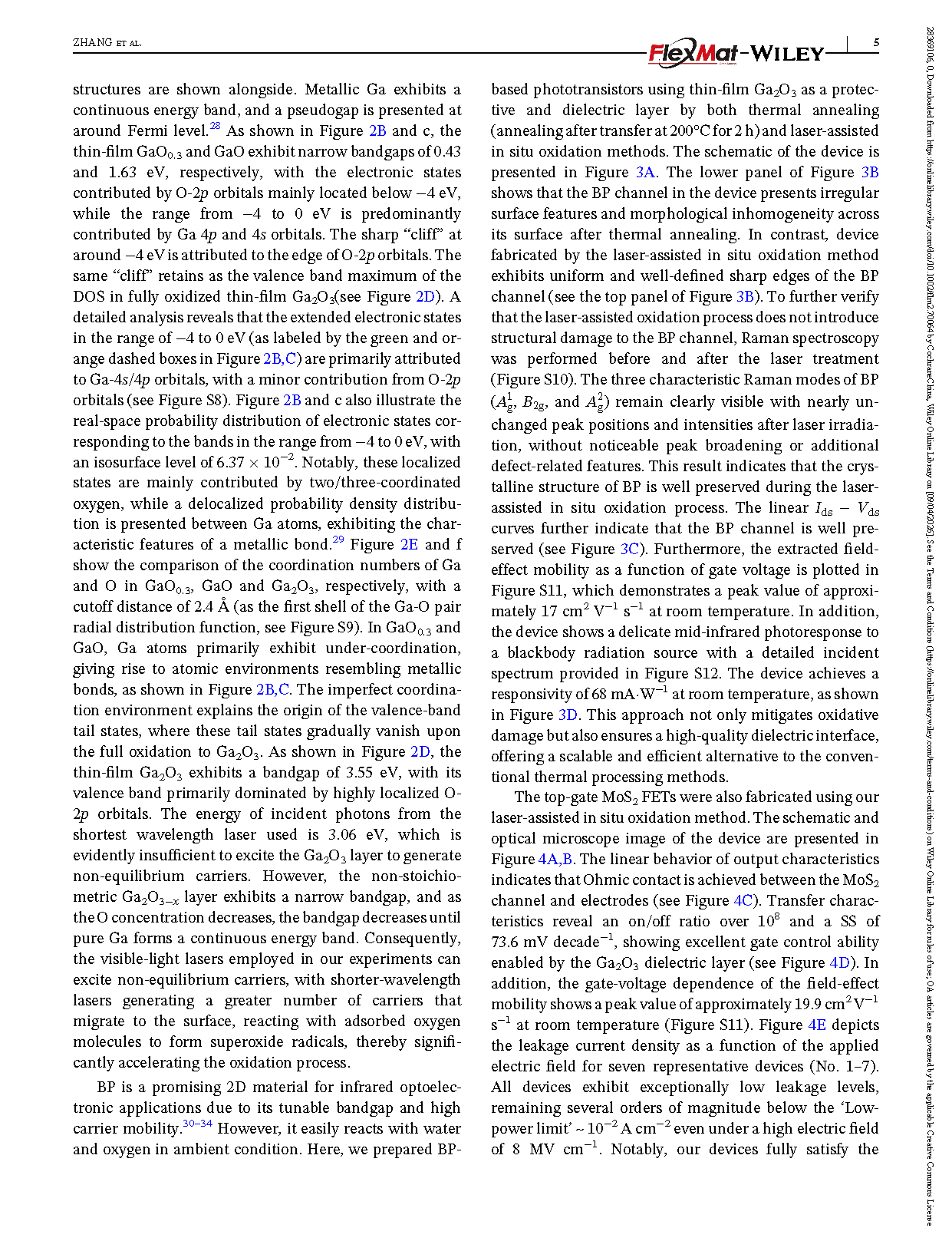
Figure 3 Characterization and infrared photoresponsivity of black phosphorus (BP) phototransistors at room temperature. (A) Schematic of the device structure of BP phototransistors. (B) Optical microscope image of BP phototransistors fabricated by laser‐assisted in situ oxidation method (top panel) and thermal annealing method (bottom panel). The device fabricated by thermal annealingmethod shows clear damage of BP channel with reduced thickness and presence of dark spots and unsharp edges. Initial BP layer isenclosed by the green dashed box. (C) Output characteristics of the BP phototransistor fabricated by laser‐assisted in situ oxidation method.(D) Infrared light response of BP phototransistor to a blackbody radiation source under various gate voltages fabricated by laser‐assisted insitu oxidation method.
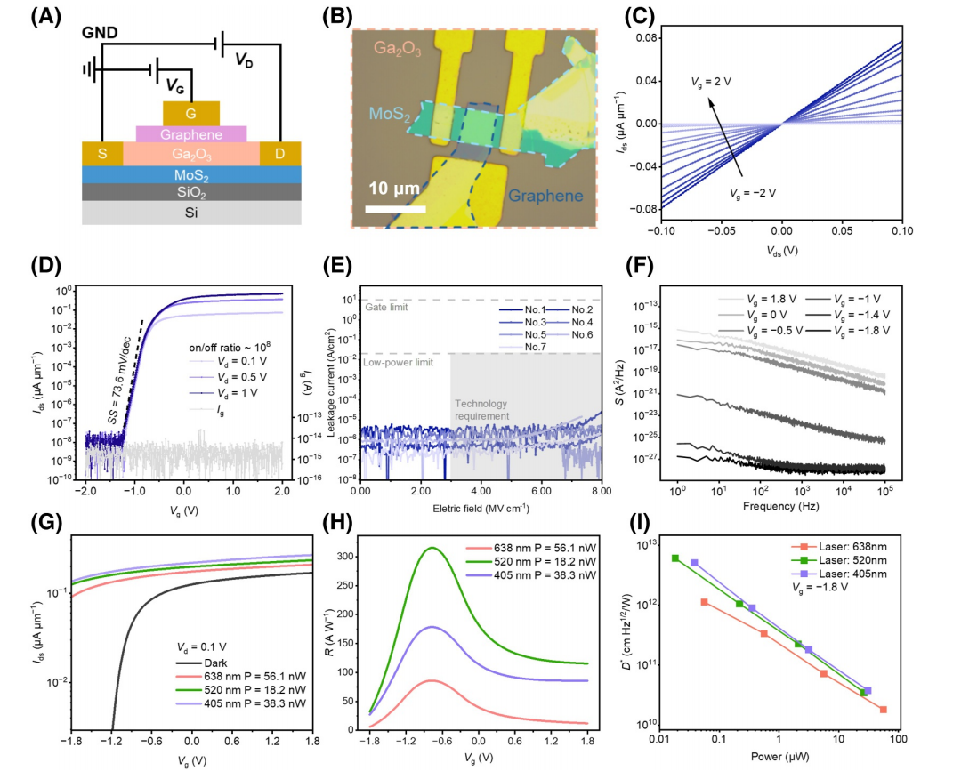
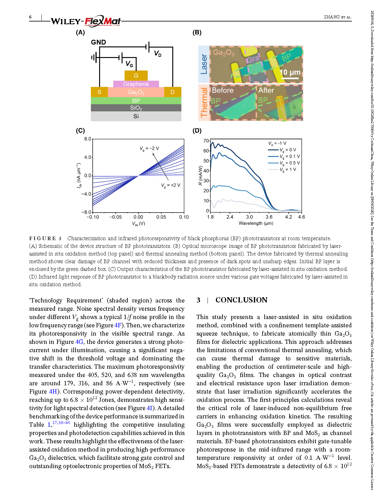
Figure 4 Characterization of the top‐gate MoS2 field‐effect transistors (FETs) with Ga2O3 dielectric fabricated by laser‐assisted oxidation method. (A) Schematic of the device structure of top-gate MoS2 FETs. (B) Optical microscope image of a fabricated top-gate MoS2 FET. (C) Output characteristics under dark condition. (D) Transfer characteristics under dark condition. (E) Current leakage of seven devices. The technology requirement, low-power limit and gate limit for the current density and breakdown field strength are from the 2022 IRDS. (F) Noise spectral density at Vds=1V under different gate voltages. (G) Transfer characteristics under various laser irradiation conditions. (H) Gate-tunable photoresponsivity under various laser irradiation conditions. (I) Power-dependent detectivity at different laser wavelengths.
DOI:
doi.org/10.1002/flm2.70064