


Discover
【Knowledge Discover】From Defect Formation Energies to Energy Level Distributions: A Graphical Interpretation of Key Semiconductor Properties
日期:2026-04-17阅读:403
Point defects are ubiquitous in materials and significantly influence their electrical, optical, and ionic transport properties, thereby playing a critical role in determining material performance in energy-related applications. First-principles calculations—particularly defect calculations based on density functional theory (DFT)—have become essential tools for predicting defect formation energies and associated electronic properties. Defect formation energy diagrams and defect level diagrams are commonly used to present these results; however, they can be difficult to interpret for researchers who are not specialists in defect physics.
Understanding defect formation energy diagrams and defect level diagrams, and learning how to extract key information from them, can be summarized as follows:
Defect and carrier concentrations
Defect formation energy diagrams can be used to predict the concentration of different defects in a material, which is crucial for understanding its electrical properties. Specifically, the formation energy of each defect varies as a function of the Fermi level (EF). By comparing the formation energies of different defects, one can identify the most stable defect under given conditions and estimate its concentration. In addition, carrier concentrations (electrons and holes) are strongly influenced by defects. Defect level diagrams provide insight into how these defects contribute to carrier concentrations, thereby affecting conductivity and other electronic properties.
Dopability
Doping is a common approach to tuning the electrical properties of semiconductors. Defect level diagrams can be used to directly evaluate whether a material is suitable for n-type or p-type doping. Dopability is closely related to defect formation energies and the positions of defect levels. Donor defects generate electrons (n-type doping), while acceptor defects generate holes (p-type doping). By analyzing the positions of defect levels at different Fermi levels, one can assess their stability and determine whether a sufficient doping window exists to achieve the desired conductivity type. This is particularly important for designing semiconductor materials for applications such as photovoltaics and electronic devices.
Mid-gap states
Mid-gap states refer to electronic levels located within the bandgap, typically introduced by defects. These states can lead to carrier recombination, reduce conductivity, or cause losses in optoelectronic performance. Defect level diagrams allow identification of these states and evaluation of their impact. If these levels lie near the center of the bandgap, they may induce significant recombination, which is detrimental to device efficiency. By comparing defect formation energies and level positions, researchers can optimize materials to minimize harmful mid-gap states.
Charge localization
Charge localization refers to the confinement of electrons or holes around defects or impurities, which can reduce conductivity and affect optical and thermal properties. Defect level diagrams help assess whether a defect induces charge localization. When defect levels lie deep within the bandgap and far from band edges, they tend to produce localized electronic states, limiting carrier mobility and resulting in low conductivity. Identifying such localized states enables further optimization of material performance, especially in sensors and electronic devices.
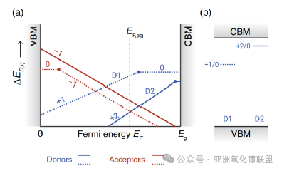
(a) Schematic of defect formation energy ED,q as a function of Fermi level EF, showing multiple defects. (b) Corresponding defect level diagram illustrating charge transition levels of defects D1 and D2 in (a).
For a given electric field (EF), the charge state with the lowest formation energy ED,q is plotted. Typically, only +1 and 0 charge states are shown, while +2 states are often omitted.
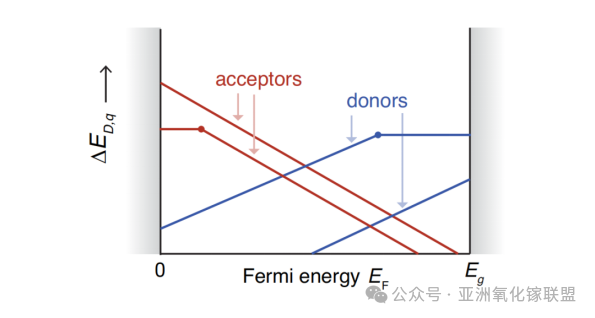
Positively charged defects (with positive slope) correspond to donor defects. Conversely, acceptor defects carry negative charge and thus exhibit negative slope lines.
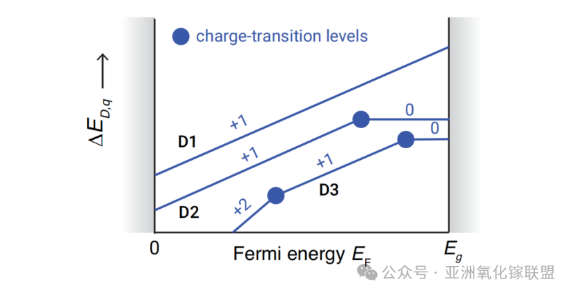
Charge transition levels of shallow and deep defects
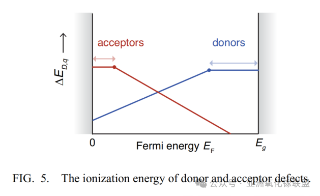
Ionization energies of donor and acceptor defects
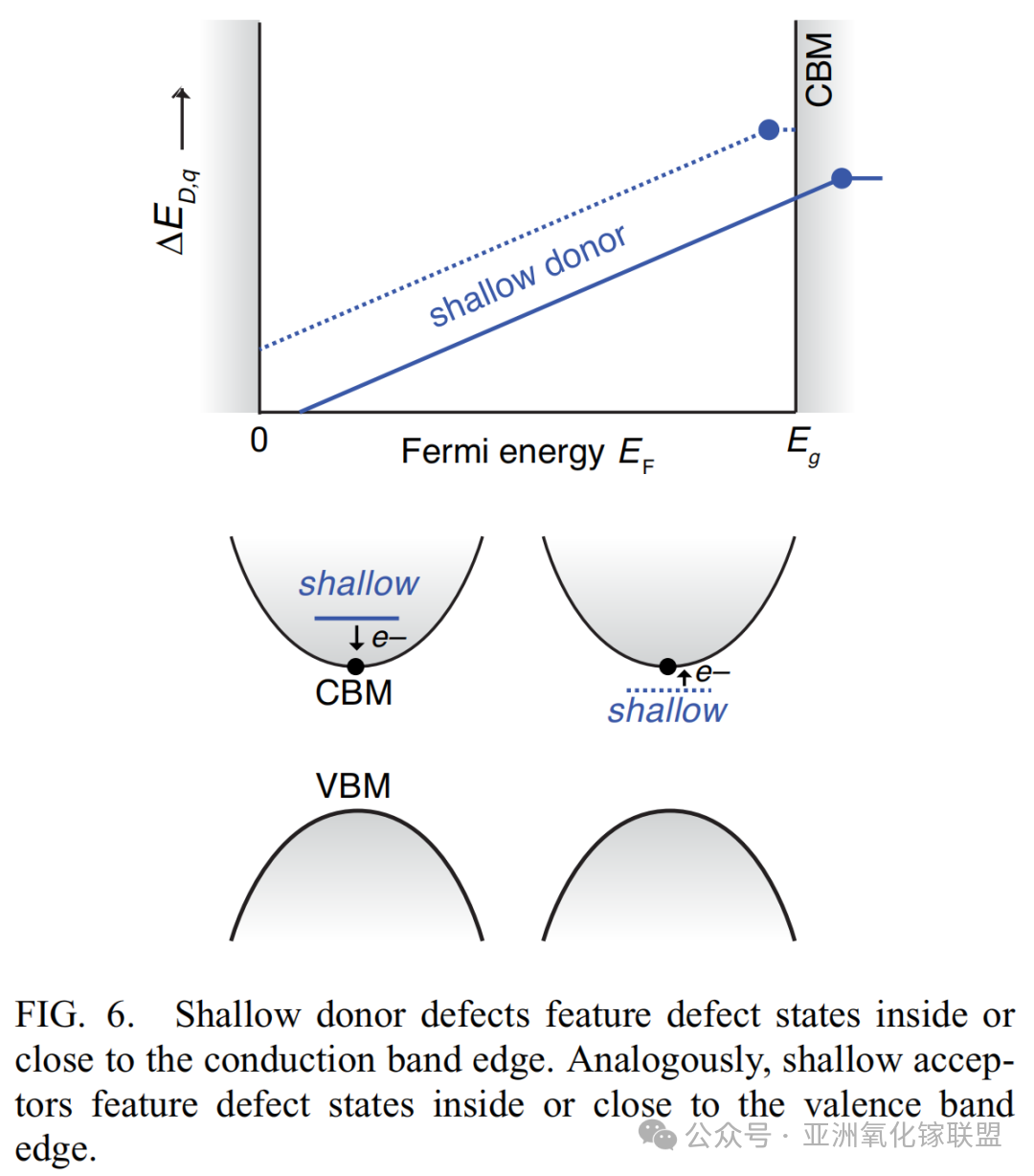
Shallow donor defects have levels located near or within the conduction band edge, while shallow acceptor defects lie near or within the valence band edge.
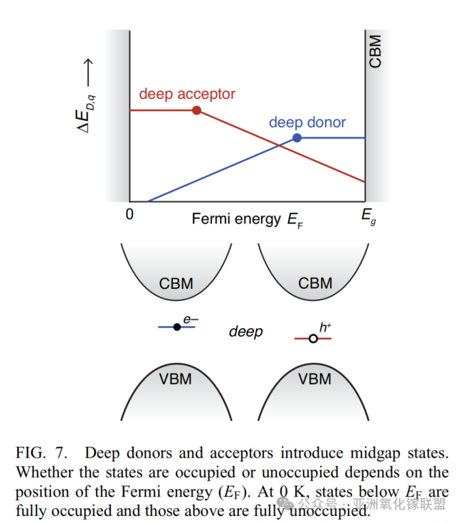
Deep donors and acceptors introduce mid-gap states. Whether these states are occupied depends on the position of the Fermi level (EF): at 0 K, all states below EF are fully occupied, while those above EF are empty.
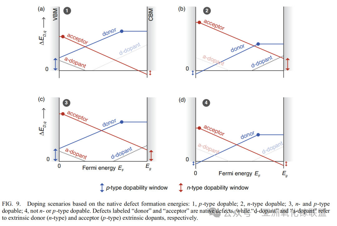
Based on intrinsic defect formation energies, doping scenarios can be categorized into four types: 1.p-type dopable 2.n-type dopable 3.both n-type and p-type dopable 4.neither n-type nor p-type dopable. Defects labeled as “donor” and “acceptor” refer to intrinsic defects, while “d-type dopants” and “a-type dopants” denote extrinsic donor (n-type) and acceptor (p-type) dopants, respectively.
Dopability and defects in β-Ga₂O₃ for power electronics
Power electronic devices require materials with high conductivity, stability, and thermal robustness. As a wide-bandgap semiconductor, β-Ga₂O₃ exhibits a high breakdown field and good high-temperature stability. Oxygen vacancies, a common defect, contribute to n-type conductivity but act as deep donor defects and therefore cannot efficiently supply free electrons. Defect formation energy diagrams reveal that these defects have relatively low formation energies, leading to high concentrations that adversely affect dopability and material stability.
Defect level analysis further shows that the observed n-type conductivity is primarily due to background impurities (such as silicon and hydrogen), rather than oxygen vacancies. Understanding these defect behaviors is crucial for the design and optimization of high-performance power electronic materials.
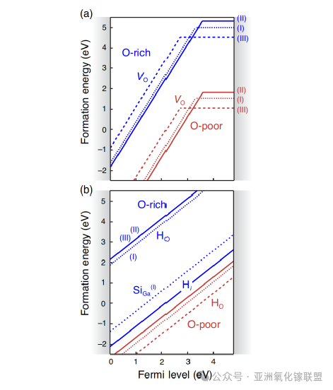
(a) Formation energies of oxygen vacancies (VO) in β-Ga₂O₃ as a function of Fermi level under oxygen-rich and oxygen-poor conditions. Labels (I), (II), and (III) correspond to three inequivalent oxygen Wyckoff sites. (b) Formation energies of hydrogen-related defects (including HO, Hi, and substitutional Si at Ga site (I)) under oxygen-rich conditions. Data reproduced from the reference.
Reference: Gorai P. Beginner’s guide to interpreting defect and defect level diagrams. PRX Energy, 2025, 4(3): 032001.
