Paper Sharing
【Member Papers】Adduct-mediated low-temperature spatial atomic layer deposition of P-type nitrogen-doped amorphous gallium oxide thin films
日期:2026-04-20阅读:48
Researchers from Xiamen University of Technology, Xiamen Institute of Measurement and Testing, Fujian Institute of Research on the Structure of Matter Chinese Academy of Sciences, National United University, National Chi Nan University and Da-Yeh University have published a dissertation titled “Adduct-mediated low-temperature spatial atomic layer deposition of P-type nitrogen-doped amorphous gallium oxide thin films” in Applied Surface Science.
Background
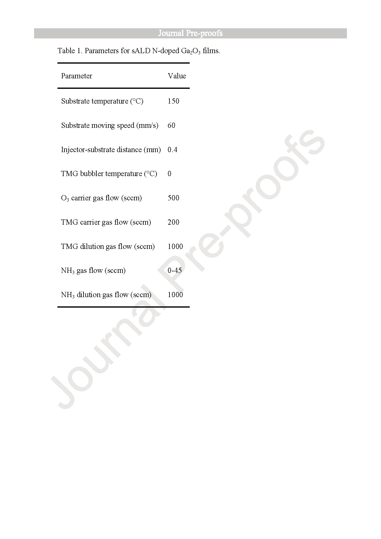
Gallium oxide (Ga₂O₃) is a promising ultra-wide bandgap semiconductor for power electronics and solar-blind optoelectronic devices, but the difficulty in realizing stable P-type conductivity limits its applications in bipolar devices and complementary circuits. Conventional N-doped Ga₂O₃ mostly relies on high-temperature processes, and effective nitrogen doping is hard to achieve at low temperatures. Spatial atomic layer deposition (sALD) enables uniform film growth at low temperatures, which is suitable for heat-sensitive and flexible devices. The team proposed an adduct-mediated strategy to prepare P-type N-doped amorphous Ga₂O₃ thin films at 150 ℃, providing a new solution for low-temperature flexible oxide electronics.
Abstract
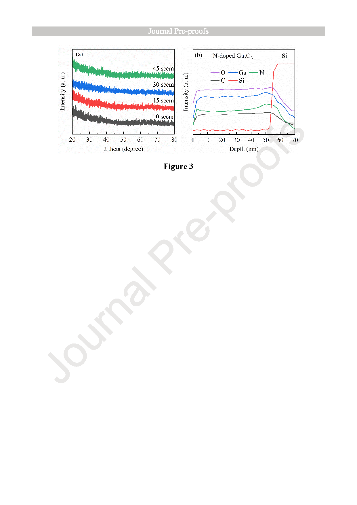
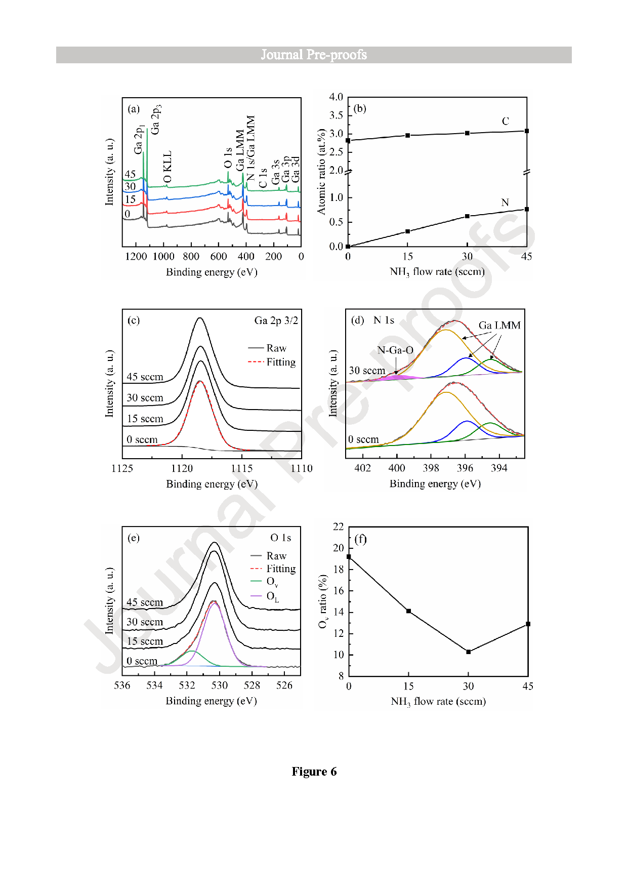
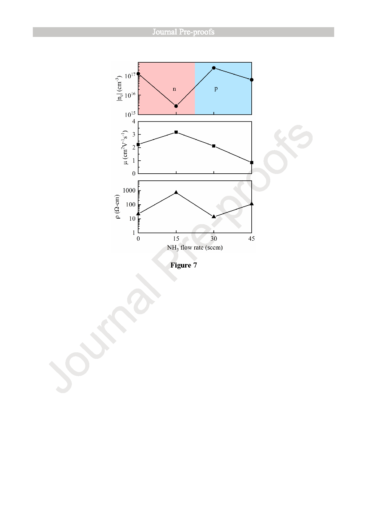
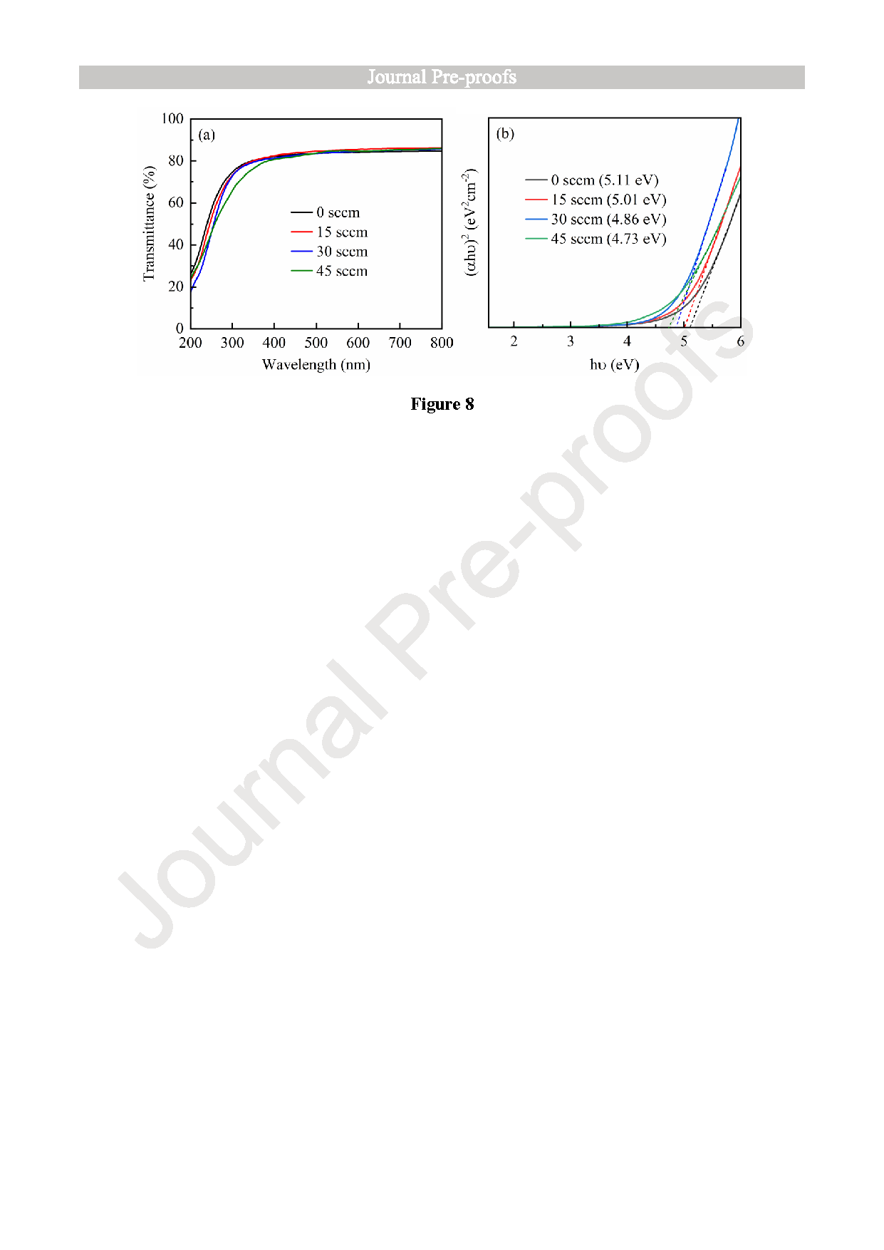
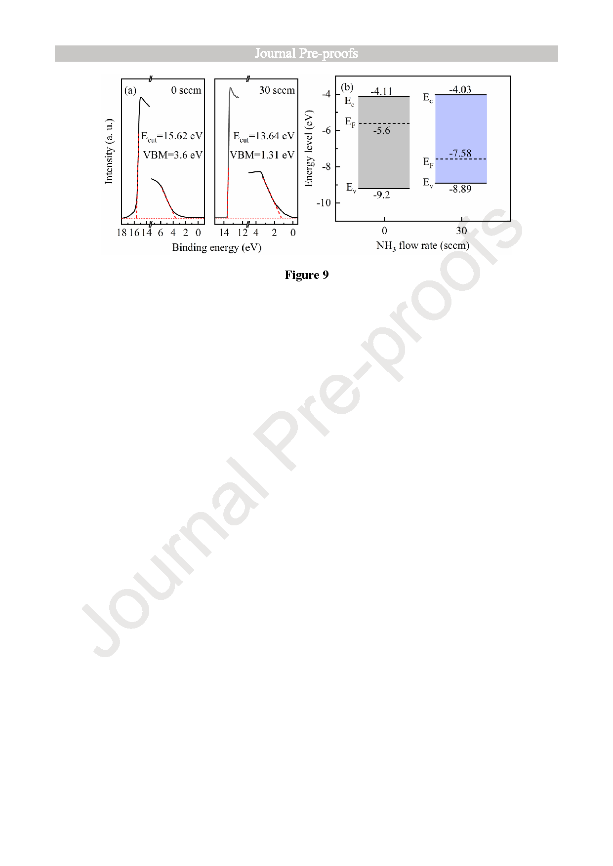
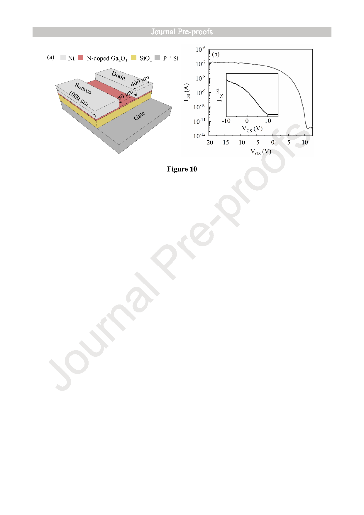
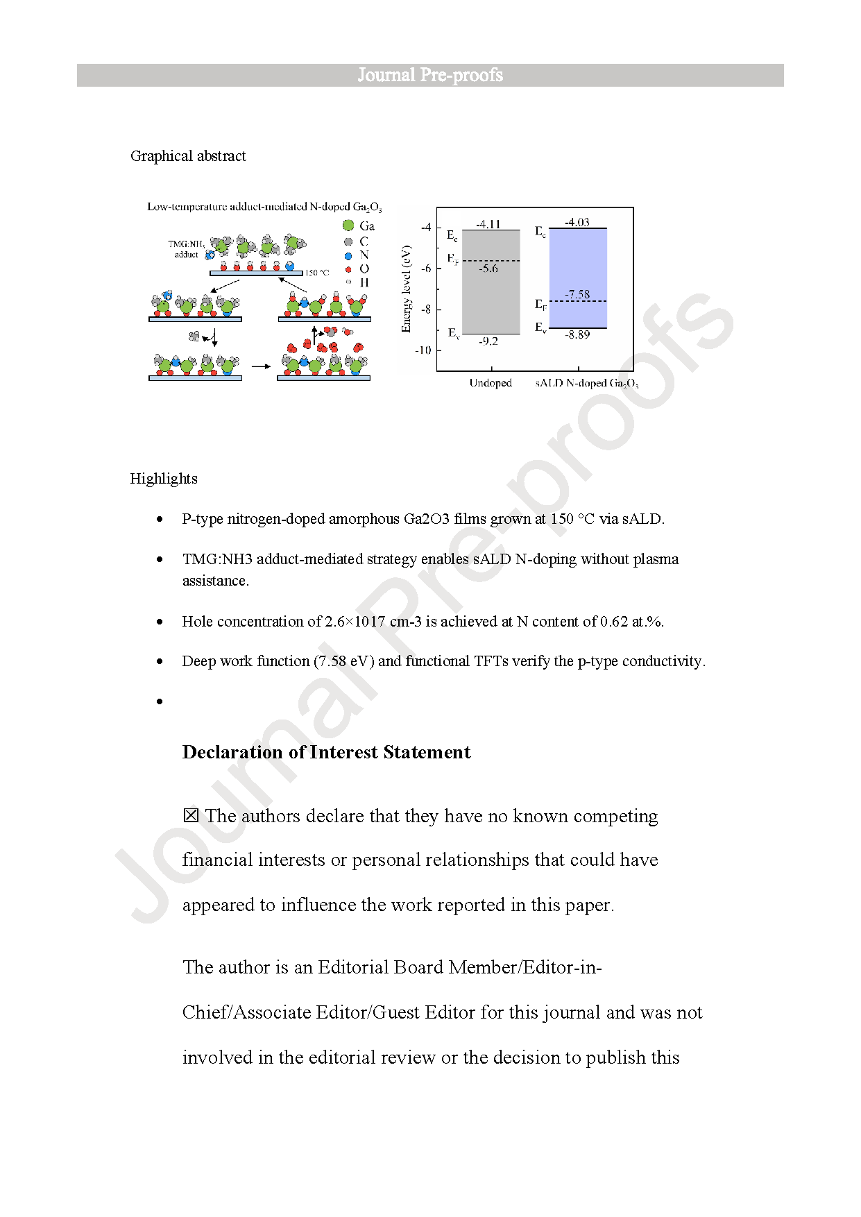
Achieving p -type conductivity in ultra-wide bandgap Ga₂O₃ under low thermal budget conditions remains a significant challenge. We report the growth of p-type nitrogen-doped amorphous Ga₂O₃ thin films at 150 °C using spatial atomic layer deposition. A precursor pre-reaction strategy utilizing Ga(CH₃)₃:NH₃ adducts is employed to overcome the high kinetic barrier of N–H bond dissociation, facilitating nitrogen incorporation without plasma assistance. Material characterization reveals that the nitrogen content increases linearly to approximately 0.62 at.% and shows slight moderation at higher precursor flows. Ultraviolet photoelectron spectra results confirm a downward shift of the Fermi level EF towards the valence band, indicating p -type electronic characteristics. Hall effect measurements identify an optimal doping window yielding a hole concentration of 2.6 ×10¹⁷ cm⁻³ and a mobility of 2.1 cm² V⁻¹ s⁻¹. This performance is attributed to the suppression of native oxygen vacancies by substitutional nitrogen. Excess precursor flow leads to mobility degradation ascribed to carrier scattering from interstitial defects induced by over-doping. A functional p-channel thin-film transistor exhibiting a current on/off ratio of 4.3 ×10⁴ is demonstrated. These results verify the feasibility of p-type conduction in amorphous oxides and provide a pathway compatible with temperature-sensitive substrates for flexible electronics.
Highlights
P-type nitrogen-doped amorphous Ga₂O₃ films grown at 150 °C via sALD.
TMG:NH₃ adduct-mediated strategy enables sALD N-doping without plasma assistance.
Hole concentration of 2.6×10¹⁷ cm⁻³ is achieved at N content of 0.62 at.%.
Deep work function (7.58 eV) and functional TFTs verify the p-type conductivity.
Conclusion
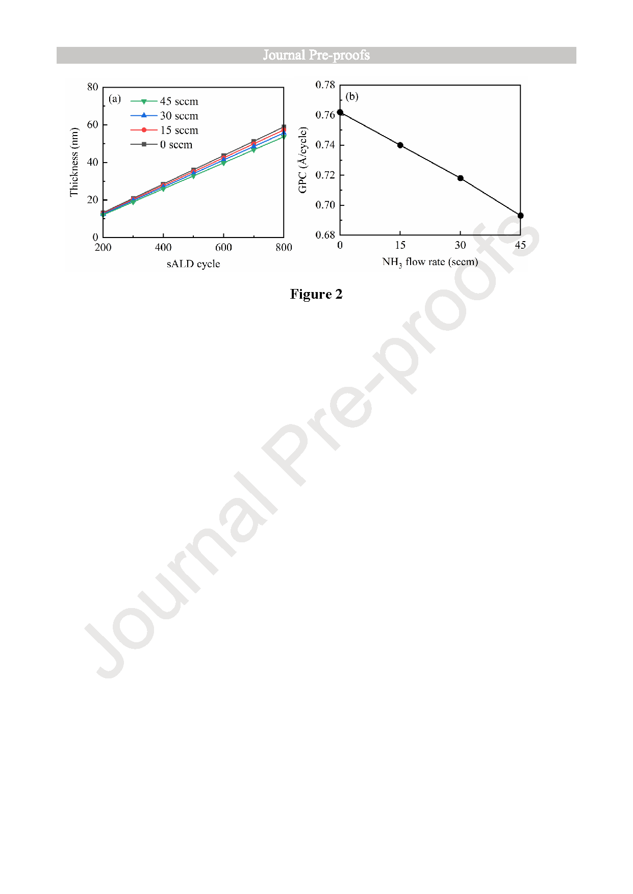
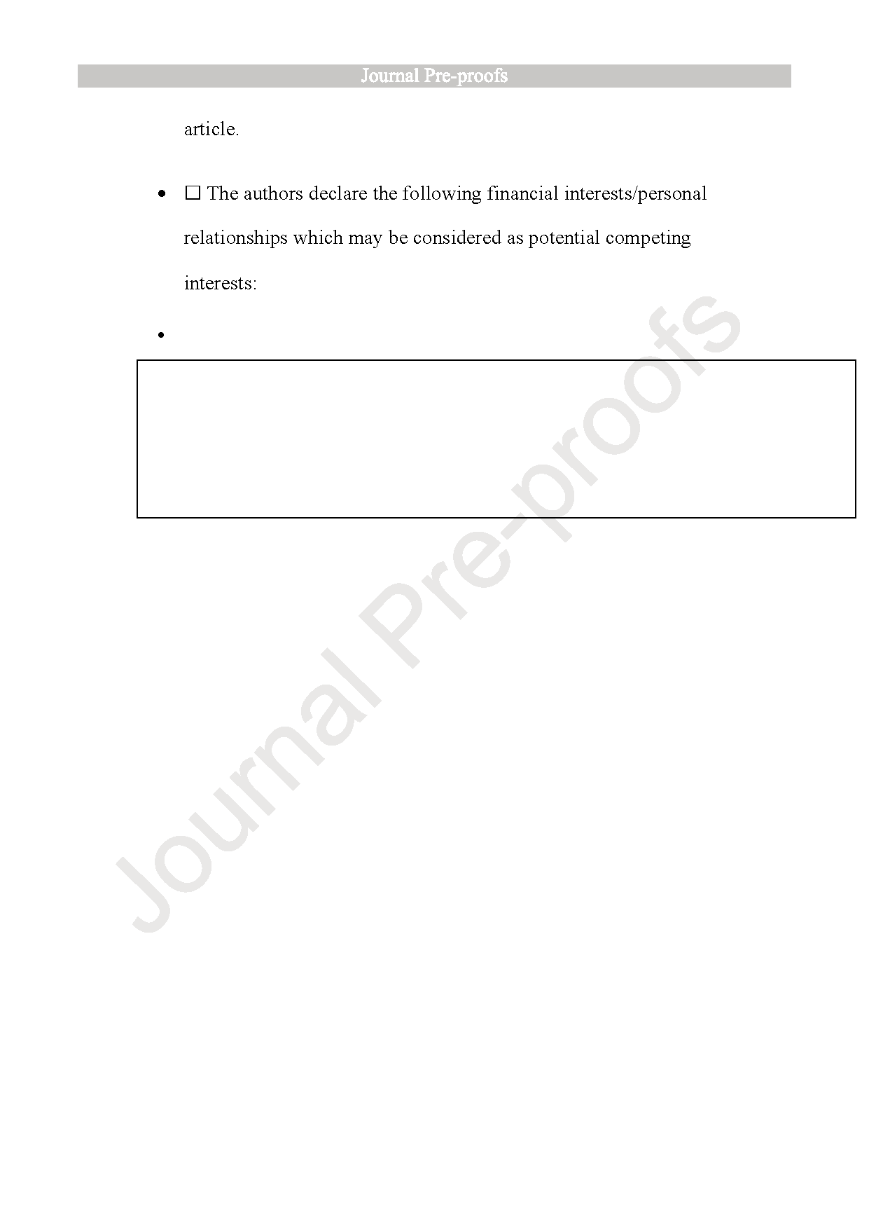
The adduct-mediated sALD is adopted for synthesizing p-type N-doped Ga₂O₃ films at 150 °C. By utilizing the pre-reaction between precursors, the thermal constraints for ammonia dissociation are successfully bypassed to enable effective doping. Growth kinetics verified a self-limiting deposition mode ideal for precise thickness control while structural characterization established that the films maintain a continuous, dense, and atomically planar amorphous morphology. Depth profiling provided definitive evidence of uniform bulk doping from the surface to the interface which rules out surface segregation effects. The optimal NH₃ flow rate of 30 sccm yields a hole concentration of 2.6 ×10¹⁷ cm⁻³ and a mobility of 2.1 cm² V⁻¹ s⁻¹, where nitrogen effectively reduce native oxygen vacancies. The systematic decrease in the oxygen-vacancy component in the O 1s spectra, the observed conductivity inversion from n-type to p-type, and the successful gate modulation of p-channel TFTs collectively indicating that the incorporated nitrogen serves as electrically active acceptors contributing to free hole generation. Higher NH₃ flow rates degrade the mobility owing to scattering from interstitial defects induced by over-doping. Electronic structure analysis revealed a distinct shift of the Fermi level towards the valence band edge which substantiates the p-type nature of the material. Finally, the successful integration of these films into a p-channel thin-film transistor with an on/off ratio of ~4.3 ×10⁴ validates the functionality of the material. This low-temperature processing route offers a robust platform for developing transparent oxide electronics on heat-sensitive polymer substrates. While in-situ spectroscopic verification (such as FTIR or mass spectrometry) would offer direct confirmation of Ga(CH₃)₃:NH₃ adduct formation and enable quantitative assessment of the kinetic barrier reduction, such experiments require specialized in-situ reaction chambers and are planned for future work.
Project Support
This work was supported by the Young and Middle-aged Teacher Education Research Project of Fujian Province (No. JAT241127); the Science and technology Project of Xiamen (No. 3502Z202373061); the National Natural Science Foundation of China (Grant No. 21975260) and the Recruitment Program of Global Experts (1000 Talents Plan) of China.
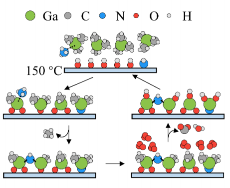
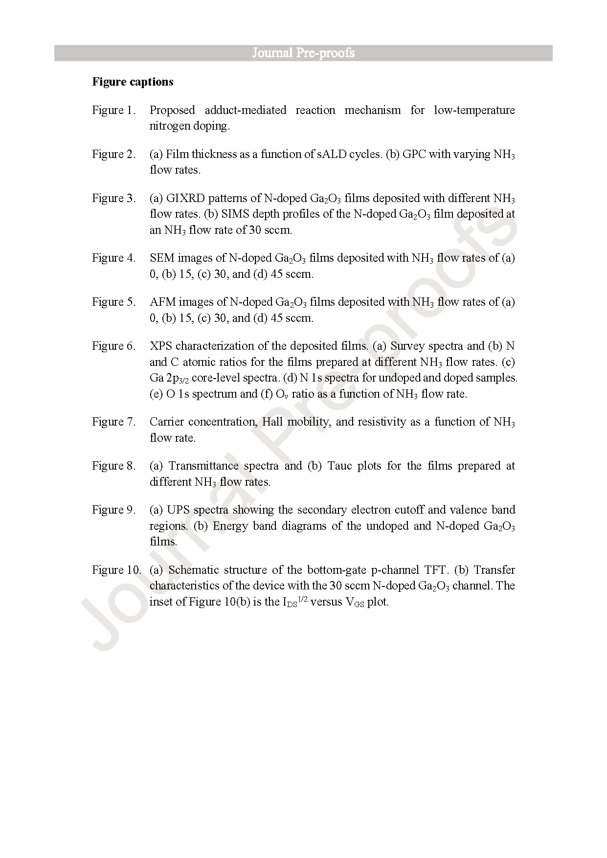
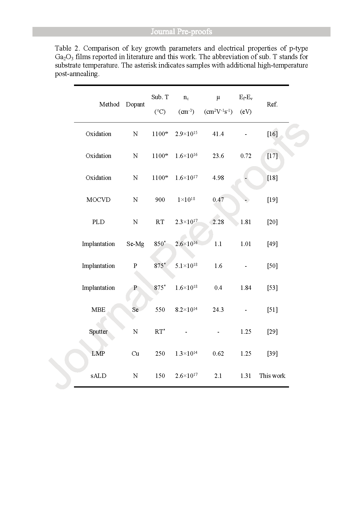
Figure 1. Proposed adduct-mediated reaction mechanism for low-temperature nitrogen doping.
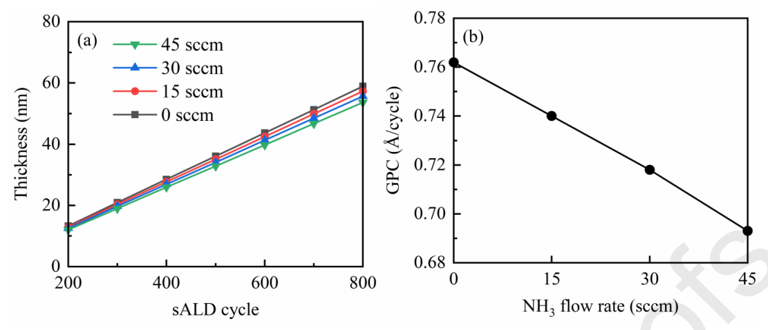
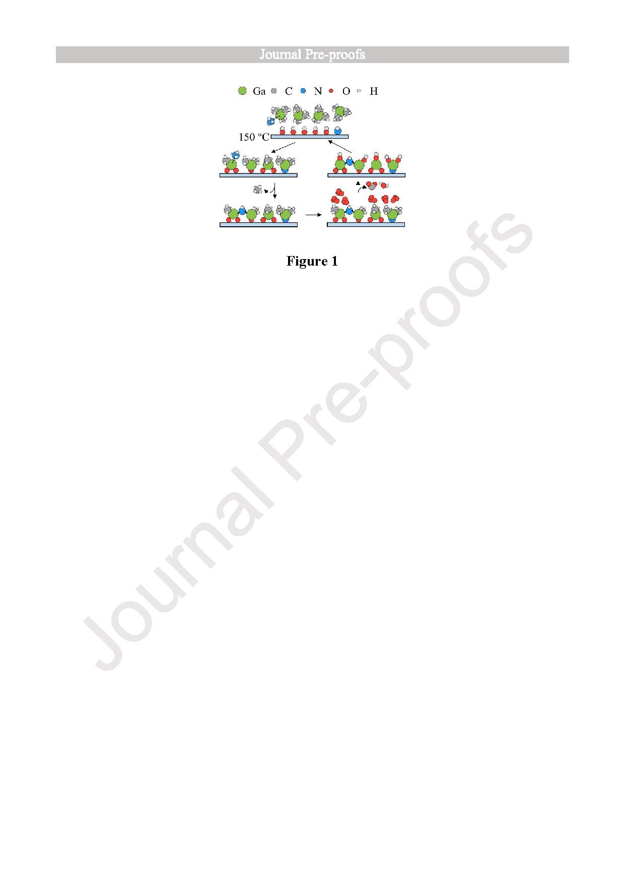
Figure 2. (a) Film thickness as a function of sALD cycles. (b) GPC with varying NH₃ flow rates.
Figure 3. (a) GIXRD patterns of N-doped Ga₂O₃ films deposited with different NH₃ flow rates. (b) SIMS depth profiles of the N-doped Ga₂O₃ film deposited at an NH₃ flow rate of 30 sccm.
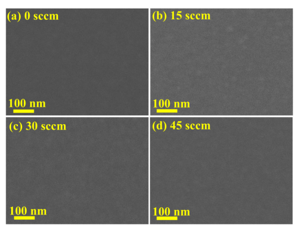
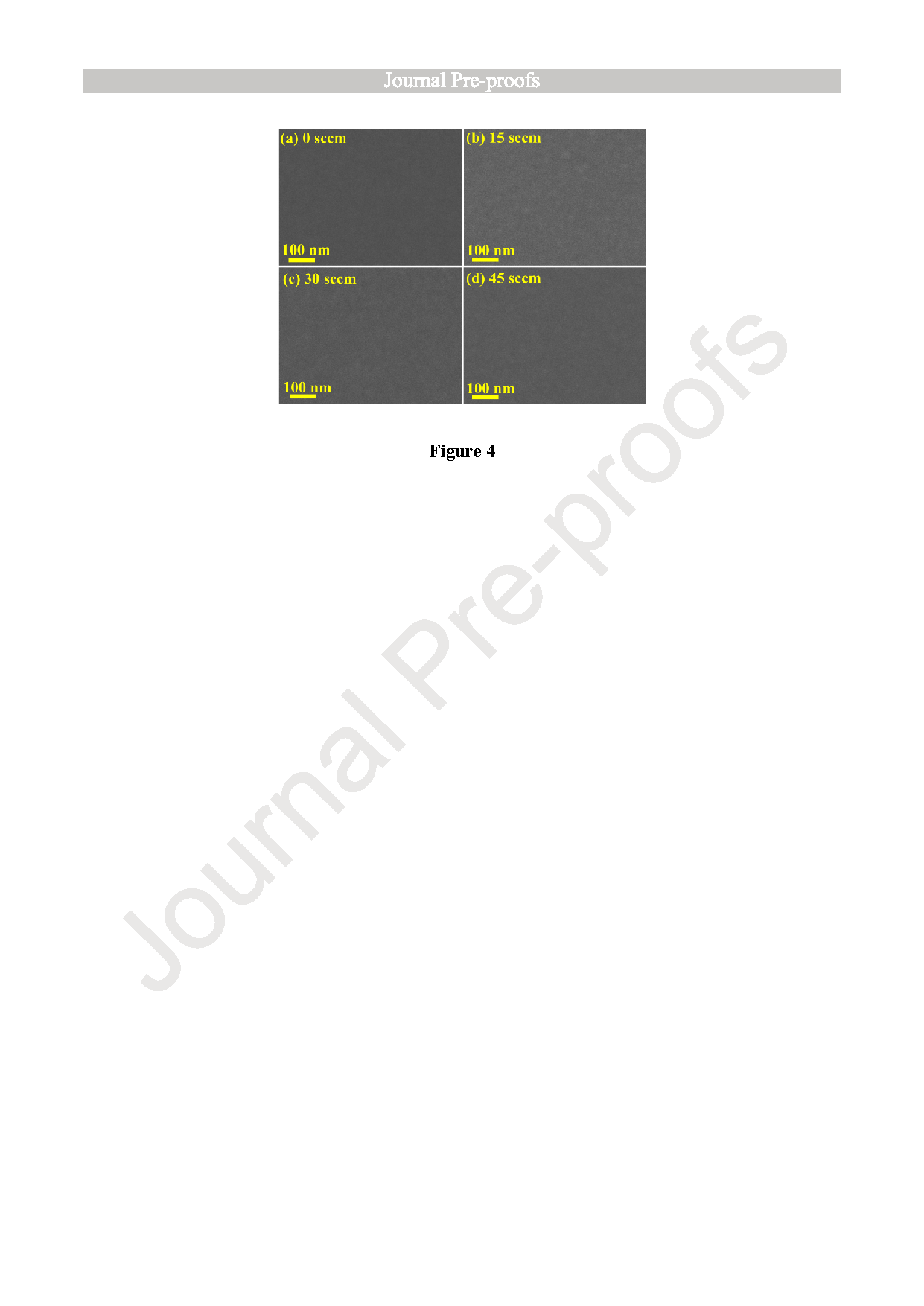
Figure 4. SEM images of N-doped Ga₂O₃ films deposited with NH₃ flow rates of (a) 0, (b) 15, (c) 30, and (d) 45 sccm.
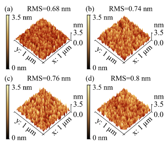
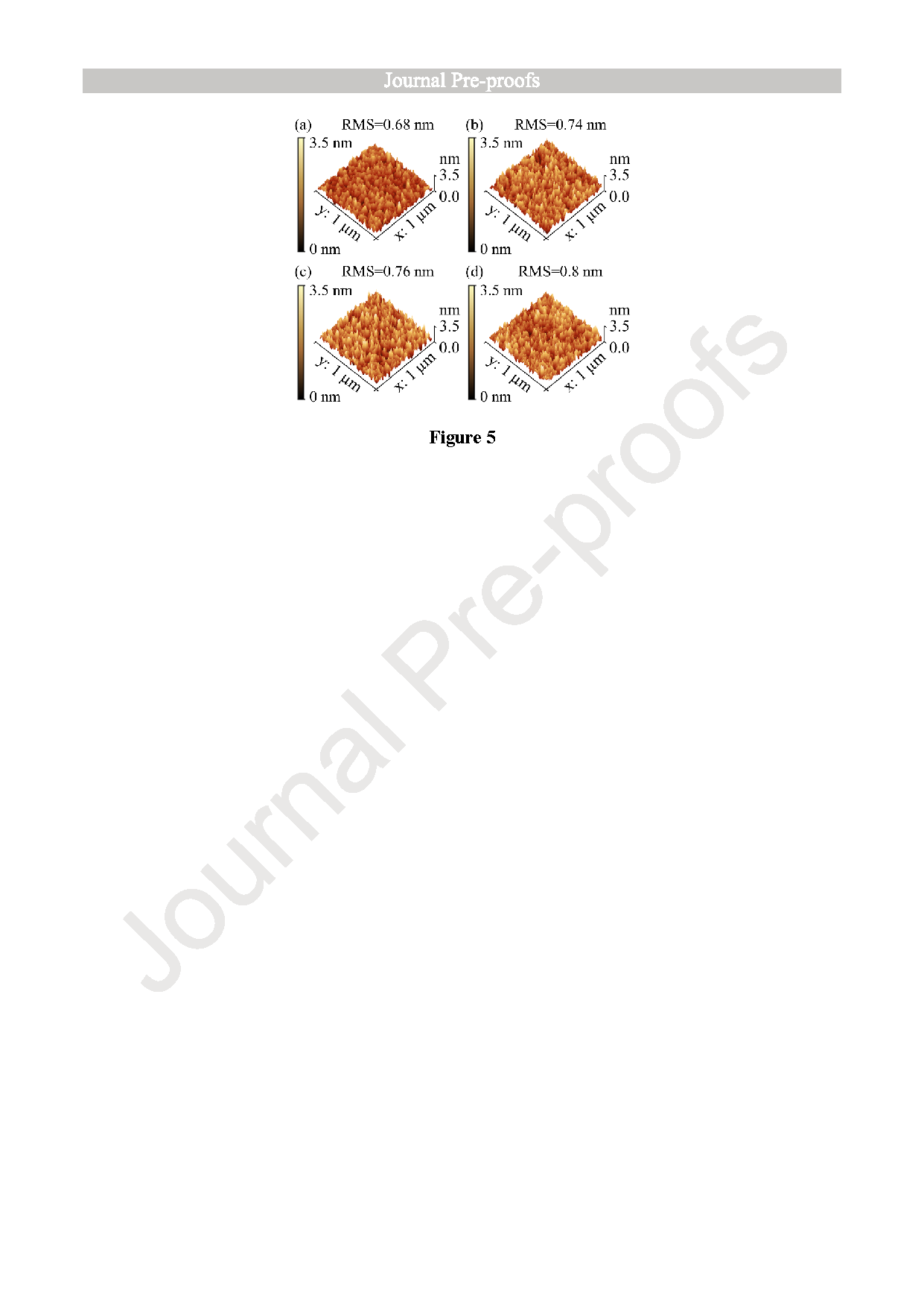
Figure 5. AFM images of N-doped Ga₂O₃ films deposited with NH₃ flow rates of (a) 0, (b) 15, (c) 30, and (d) 45 sccm.
DOI:
doi.org/10.1016/j.apsusc.2026.166803