Paper Sharing
【Member Papers】Lattice orientation preferred dual-wavelength photoresponse characteristics of β Ga₂O₃/GeO₂ heterostructures for high-performance solar-blind photodetectors
日期:2026-04-21阅读:47
Researchers from the Ningbo University, Guilin University of Electronic Technology, Beijing University of Posts and Telecommunications, Nanjing University of Posts and Telecommunications have published a dissertation titled "Lattice orientation preferred dual-wavelength photoresponse characteristics of β‑Ga₂O₃/GeO₂ heterostructures for high-performance solar-blind photodetectors" in Applied Surface Science.
Background
Solar-blind photodetectors (SBPDs) based on β‑Ga₂O₃ heterojunctions have enormous potential in next-generation multifunctional optoelectronic devices. However, the lack of bandgap-matched partners for ultra-wide bandgap β‑Ga₂O₃ leads to undesired out-of-band absorption and broadband responses in conventional heterojunction SBPDs. In this work, heterostructures combining hexagonal GeO₂ with (-201) and (310)-oriented Ga₂O₃ are used to develop high-performance dual-wavelength SBPDs.
Abstract
Solar-blind photodetectors (SBPDs) based on β‑Ga₂O₃ heterojunctions have demonstrated enormous potential applications in the development of next-generation multifunctional optoelectronic devices. However, the scarcity of bandgap-matched partners for the ultra-wide bandgap semiconductor β‑Ga₂O₃ leads to undesired out-of-band absorption and broadband responses in conventional heterojunction SBPDs. Here, heterostructures constructed by combining hexagonal GeO₂ with (-201) and (310)-oriented Ga₂O₃ have been utilized to develop high-performance dual-wavelength SBPDs. Relative to the intrinsic β‑Ga₂O₃ device, the (310)-oriented β‑Ga₂O₃/GeO₂ heterojunction SBPD exhibits significant improvement in photoresponse characteristics including 15 and 100 times increases in the photocurrent-to-dark-current ratio and over 4 orders of magnitude of enhancement in the external quantum efficiency at 254 and 213 nm, respectively. These excellent performances are primarily attributed to the more favorable type-II band alignments at the interface of Ga₂O₃ and GeO₂ films, which establishes an effective built-in electric field with a potential difference of ~42.2 meV to promote carrier separation and transport. On the foundation of (310)-oriented heterojunction SBPDs, binary encoded optical signal transmissions and reconfigurable optoelectronic logic gates with bias-voltage and optical inputs have been successfully realized at dual solar-blind wavelength. The proposed engineered β‑Ga₂O₃/GeO₂ heterostructures provides a general route to develop high-performance SBPDs for scalable solar-blind imaging/processing technologies.
Highlights
Realize (-201)/(310)-oriented β‑Ga₂O₃/GeO₂ heterostructures with dual-wavelength (213 nm/254 nm) solar-blind photoresponse.
(310)-oriented heterojunction forms type-II band alignment and strong built-in electric field, greatly improving carrier separation efficiency.
Key performances including photocurrent-to-dark-current ratio, EQE and detectivity are improved by orders of magnitude.
Successfully realize solar-blind optoelectronic logic operations and binary optical signal transmission.
Conclusion
As a summary, we have successfully designed to fabricate Ga₂O₃/GeO₂ heterojunction SBPDs and systematically described the effect of (-201) and (310) lattice planes of the β‑Ga₂O₃ films on device performances of heterojunction SBPDs in this work. The demonstrated type‑II band alignments in both Ga₂O₃/GeO₂ heterojunction SBPDs possess obvious built‑in electric fields at the G3S40 and G2S40 interfaces, corresponding to the effective charge transfer quantity of around 0.59 and 0.02 e from Ga₂O₃ to GeO₂ layers. The efficient separation photo‑generated carriers induced by the existent of built‑in electric fields in SBPDs enable boosted 254 and 213 nm photoresponses, in which the G3S40 SBPD exhibits more excellent device performances including a higher PDCR of 2.4×10⁴(1.5×10⁵), a greater EQE of 275 (538.96) %, a stronger R of 4.7×10⁻¹(0.97) A W⁻¹, and a higher D* of 2.1×10¹²(1.99×10¹³) Jones at 254 (213) nm, respectively. Based on the better photodetection capabilities, the G3S40 SBPD is employed to effectively implement reconfigurable “AND” and “OR” logic functions and also demonstrate its potential for next‑generation solar‑blind imaging and multifunctional optoelectronic systems. As a result, our findings establish the Ga₂O₃/GeO₂ heterojunction as a promising solar‑blind UV photodetector candidate and provide a foundation for the development and production of high‑performance optoelectronic devices.
Project Support
This work was supported by the Natural Science Foundation of China (Grant No. 62204130) and Yongjiang talents program with No. 2022 A‑218‑G.
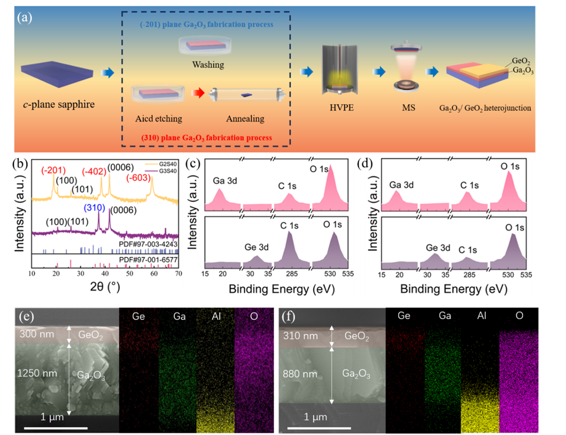
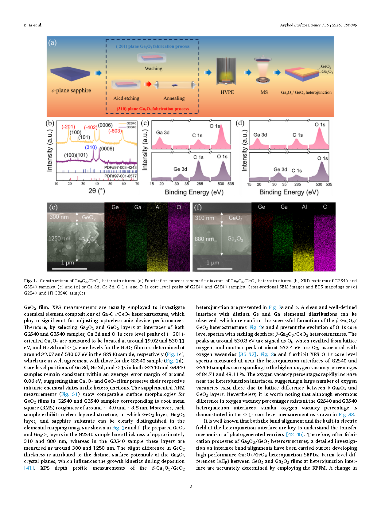
Figure 1 Constructions of Ga₂O₃/GeO₂ heterostructures. (a) Fabrication process schematic diagram of Ga₂O₃/GeO₂ heterostructures. (b) XRD patterns of G2S40 and G3S40 samples. (c) and (d) of Ga 3d, Ge 3d, C 1s, and O 1s core level peaks of G2S40 and G3S40 samples. Cross-sectional SEM images and EDS mappings of (e) G2S40 and (f) G3S40 samples.
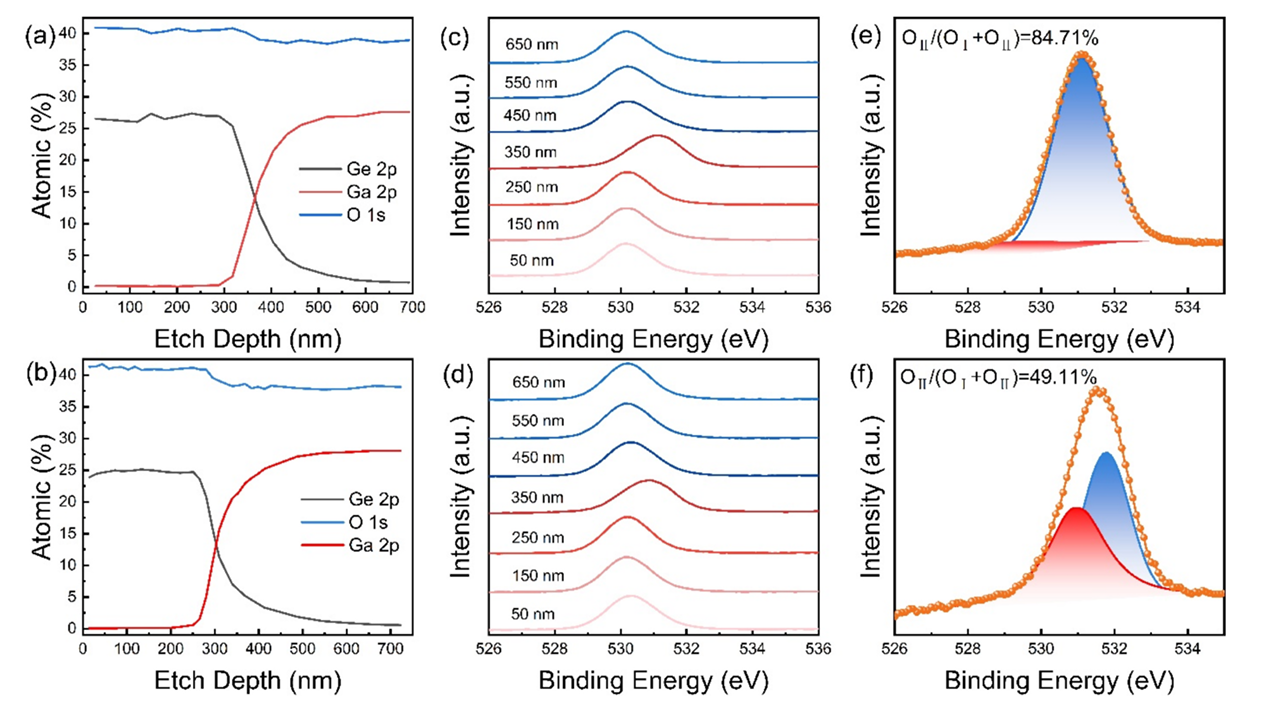
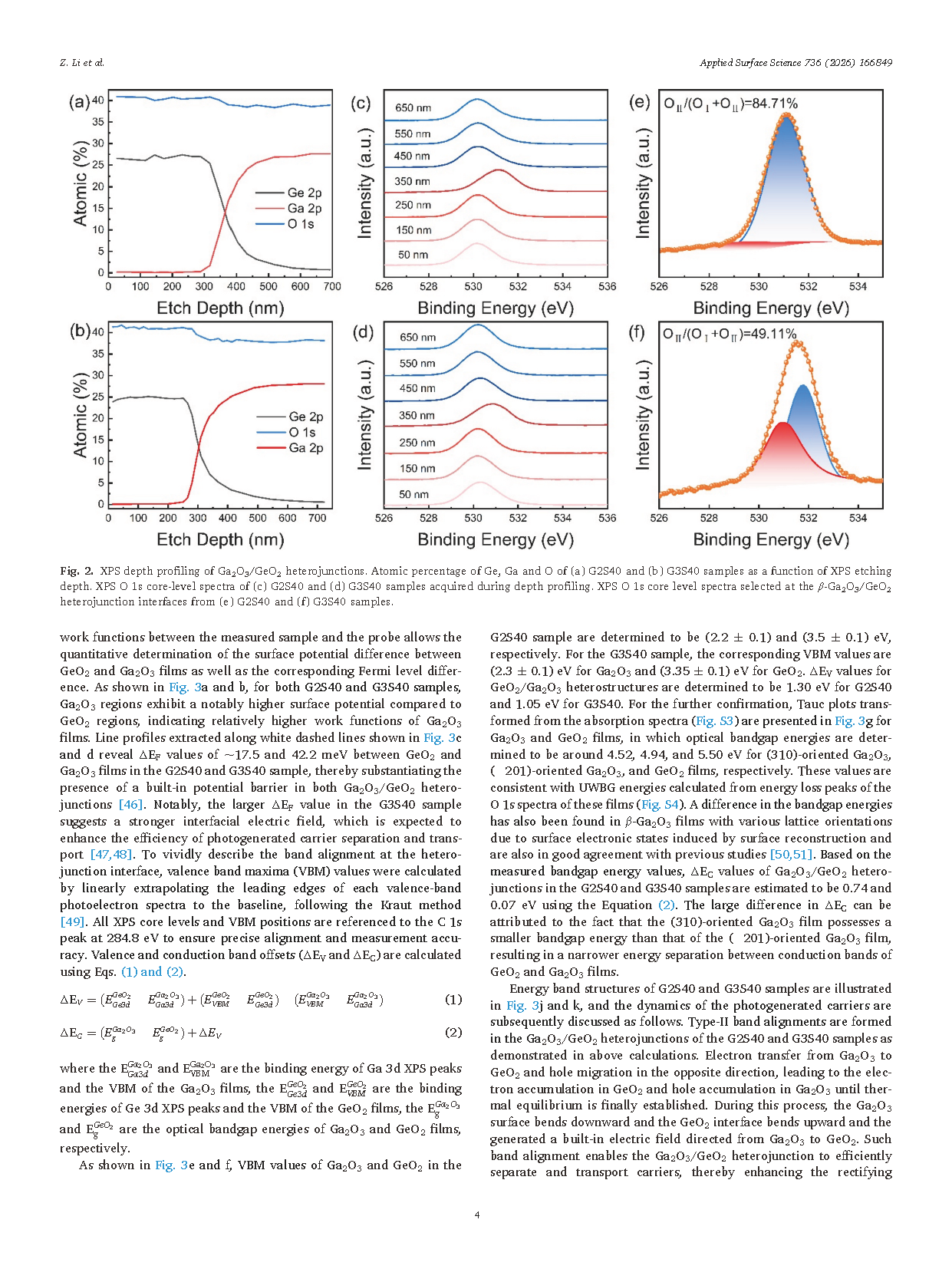
Figure 2 XPS depth profiling of Ga₂O₃/GeO₂ heterojunctions. Atomic percentage of Ge, Ga and O of (a) G2S40 and (b) G3S40 samples as a function of XPS etching depth. XPS O 1s core-level spectra of (c) G2S40 and (d) G3S40 samples acquired during depth profiling. XPS O 1s core level spectra selected at the β‑Ga₂O₃/GeO₂ heterojunction interfaces from (e) G2S40 and (f) G3S40 samples.
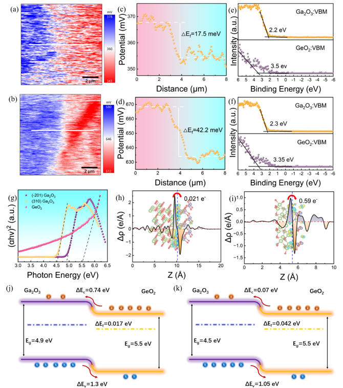
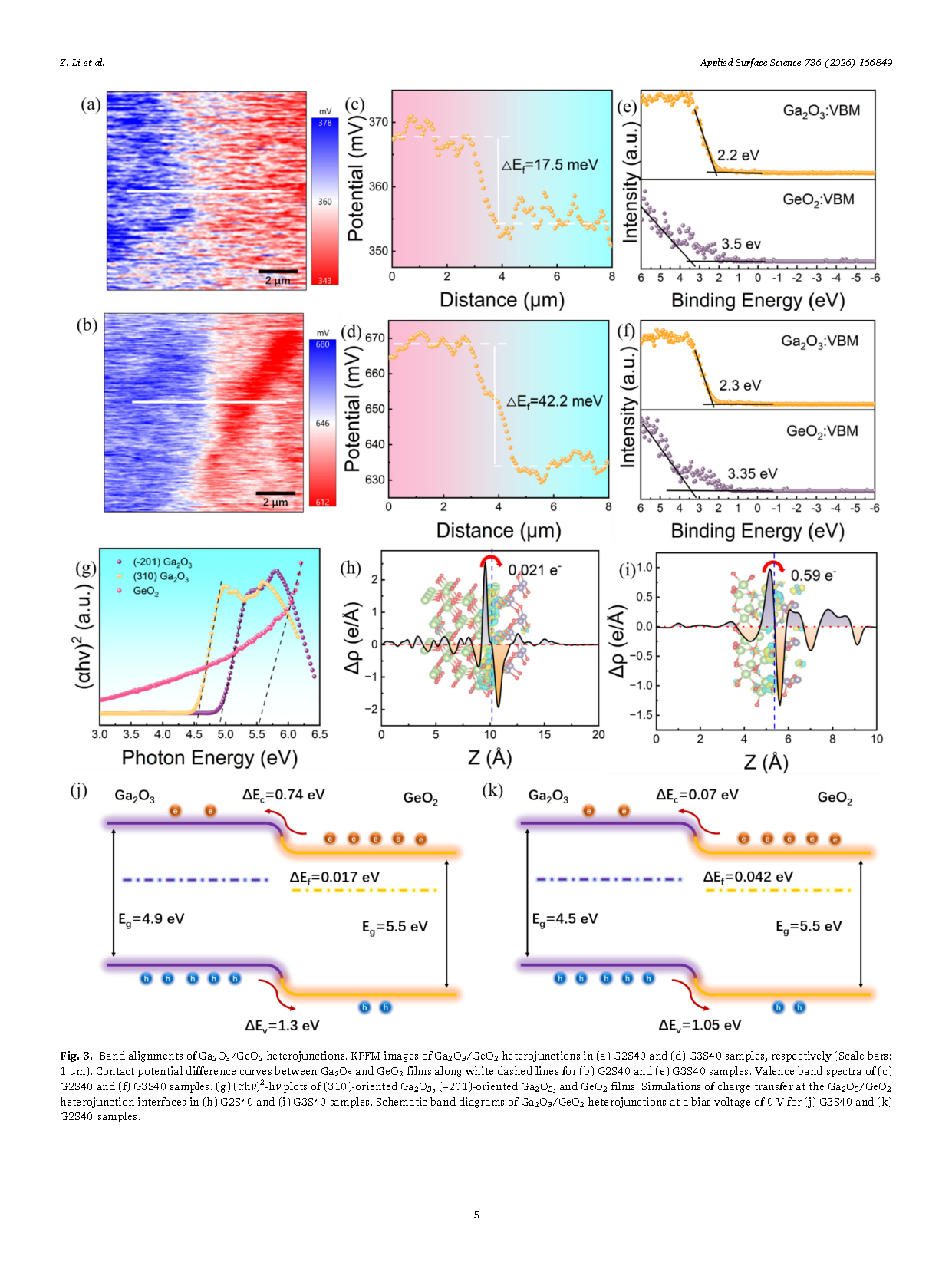
Figure 3 Band alignments of Ga₂O₃/GeO₂ heterojunctions. KPFM images of Ga₂O₃/GeO₂ heterojunctions in (a) G2S40 and (d) G3S40 samples, respectively (Scale bars: 1 μm). Contact potential difference curves between Ga₂O₃ and GeO₂ films along white dashed lines for (b) G2S40 and (e) G3S40 samples. Valence band spectra of (c) G2S40 and (f) G3S40 samples. (g) (αhν)²‑hν plots of (310)‑oriented Ga₂O₃, (-201)‑oriented Ga₂O₃, and GeO₂ films. Simulations of charge transfer at the Ga₂O₃/GeO₂ heterojunction interfaces in (h) G2S40 and (i) G3S40 samples. Schematic band diagrams of Ga₂O₃/GeO₂ heterojunctions at a bias voltage of 0 V for (j) G3S40 and (k) G2S40 samples.
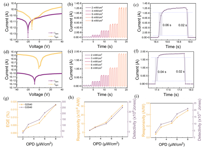
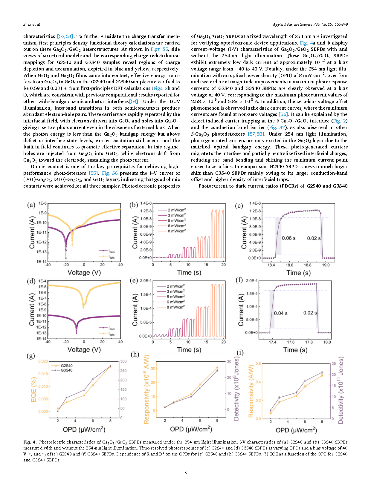
Figure 4 Photoelectric characteristics of Ga₂O₃/GeO₂ SBPDs measured under the 254 nm light illumination. I‑V characteristics of (a) G2S40 and (b) G3S40 SBPDs measured with and without the 254‑nm light illumination. Time‑resolved photoresponses of (c) G2S40 and (d) G3S40 SBPDs at varying OPDs and a bias voltage of 40 V. τᵣ and τd of (e) G2S40 and (f) G3S40 SBPDs. Dependence of R and D* on the OPDs for (g) G2S40 and (h) G3S40 SBPDs. (i) EQE as a function of the OPD for G2S40 and G3S40 SBPDs.
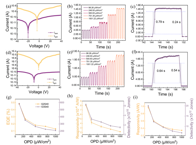
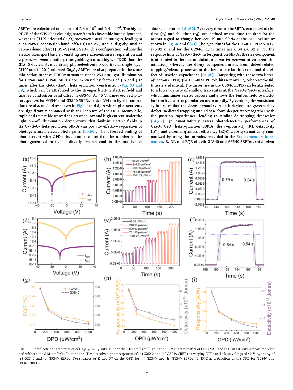
Figure 5 Photoelectric characteristics of Ga₂O₃/GeO₂ SBPDs under the 213‑nm light illumination. I‑V characteristics of (a) G2S40 and (b) G3S40 SBPDs measured with and without the 213‑nm light illumination. Time‑resolved photoresponses of (c) G2S40 and (d) G3S40 SBPDs at varying OPDs and a bias voltage of 40 V. τᵣ and τd of (e) G2S40 and (f) G3S40 SBPDs. Dependence of R and D* on the OPD for (g) G2S40 and (h) G3S40 SBPDs. (i) EQE as a function of the OPD for G2S40 and G3S40 SBPDs.
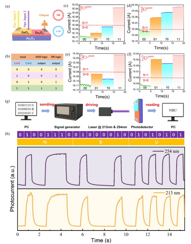
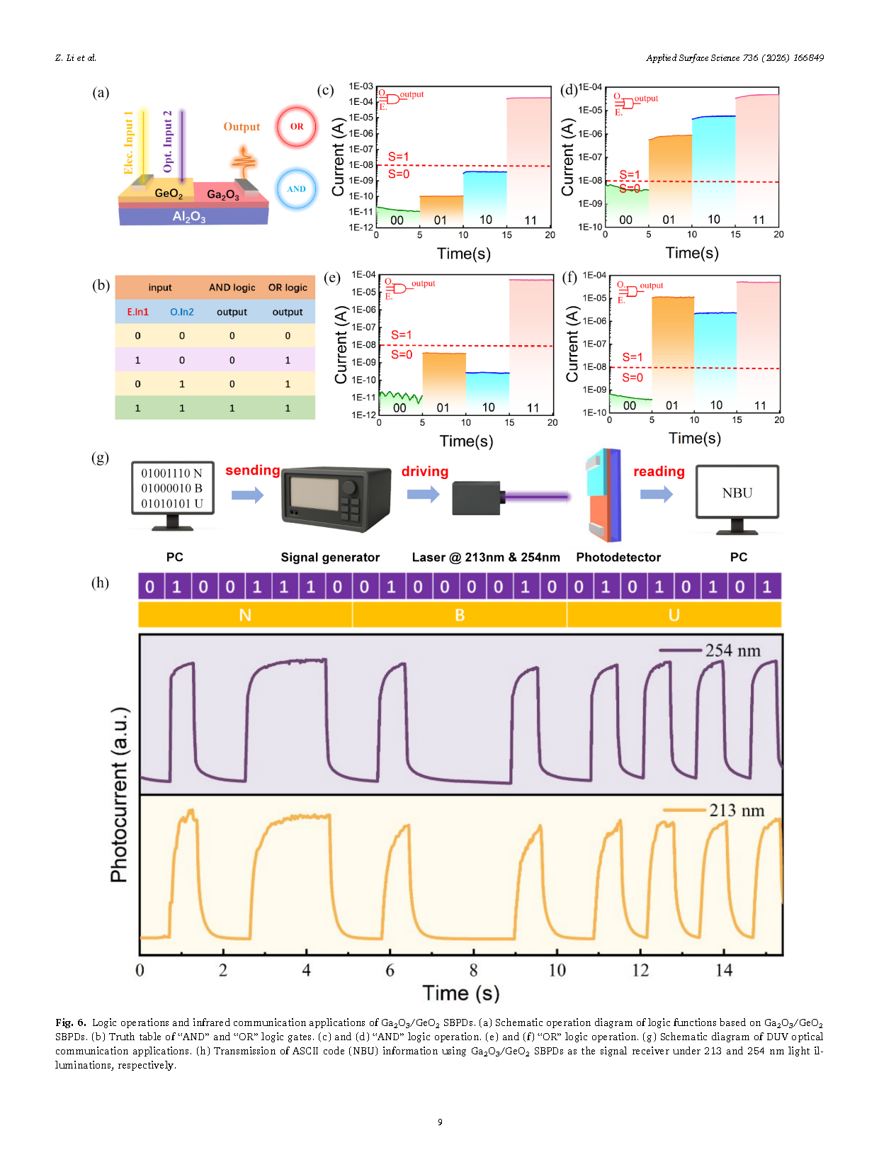
Figure 6 Logic operations and infrared communication applications of Ga₂O₃/GeO₂ SBPDs. (a) Schematic operation diagram of logic functions based on Ga₂O₃/GeO₂ SBPDs. (b) Truth table of “AND” and “OR” logic gates. (c) and (d) “AND” logic operation. (e) and (f) “OR” logic operation. (g) Schematic diagram of DUV optical communication applications. (h) Transmission of ASCII code (NBU) information using Ga₂O₃/GeO₂ SBPDs as the signal receiver under 213 and 254 nm light illuminations, respectively.
DOI:
doi. org/10.1016/j.apsusc.2026.166849