Paper Sharing
【International Papers】Morphology investigation of metalorganic vapor phase epitaxy homoepitaxial (001) β-Ga₂O₃ growth on on-axis and 6° off-axis substrates
日期:2026-04-22阅读:133
Researchers from Leibniz-Institut für Kristallzüchtung (IKZ) have published a dissertation titled “Morphology investigation of metalorganic vapor phase epitaxy homoepitaxial (001) β‑Ga₂O₃ growth on on-axis and 6° off-axis substrates” in Journal of Vacuum Science & Technology A.
Background
As power electronics advance, β-Ga₂O₃ (gallium oxide) has emerged as a potential fourth-generation semiconductor due to its ultrawide bandgap (4.85 eV) and high electric breakdown field (8 MV/cm). Unlike other wide-bandgap materials like SiC and GaN, β-Ga₂O₃ can be produced using cost-effective, high-volume melt-growth methods such as Czochralski and edge-defined film-fed growth (EFG). Among various growth techniques, Metalorganic Vapor Phase Epitaxy (MOVPE) stands out for its scalability in commercial applications. While research has progressed on (100) and (010) crystal planes, systematic studies on the (001) plane remain limited due to challenges like twin formation, limited adatom diffusivity, and surface roughness. Since the (001) orientation supports large-diameter wafers and shares cleavage properties with the (100) plane, this study applies successful (100) growth strategies—specifically introducing substrate miscuts and fine-tuning Ga supersaturation—to investigate and optimize the morphology of homoepitaxial (001) β-Ga₂O₃ layers.
Abstract
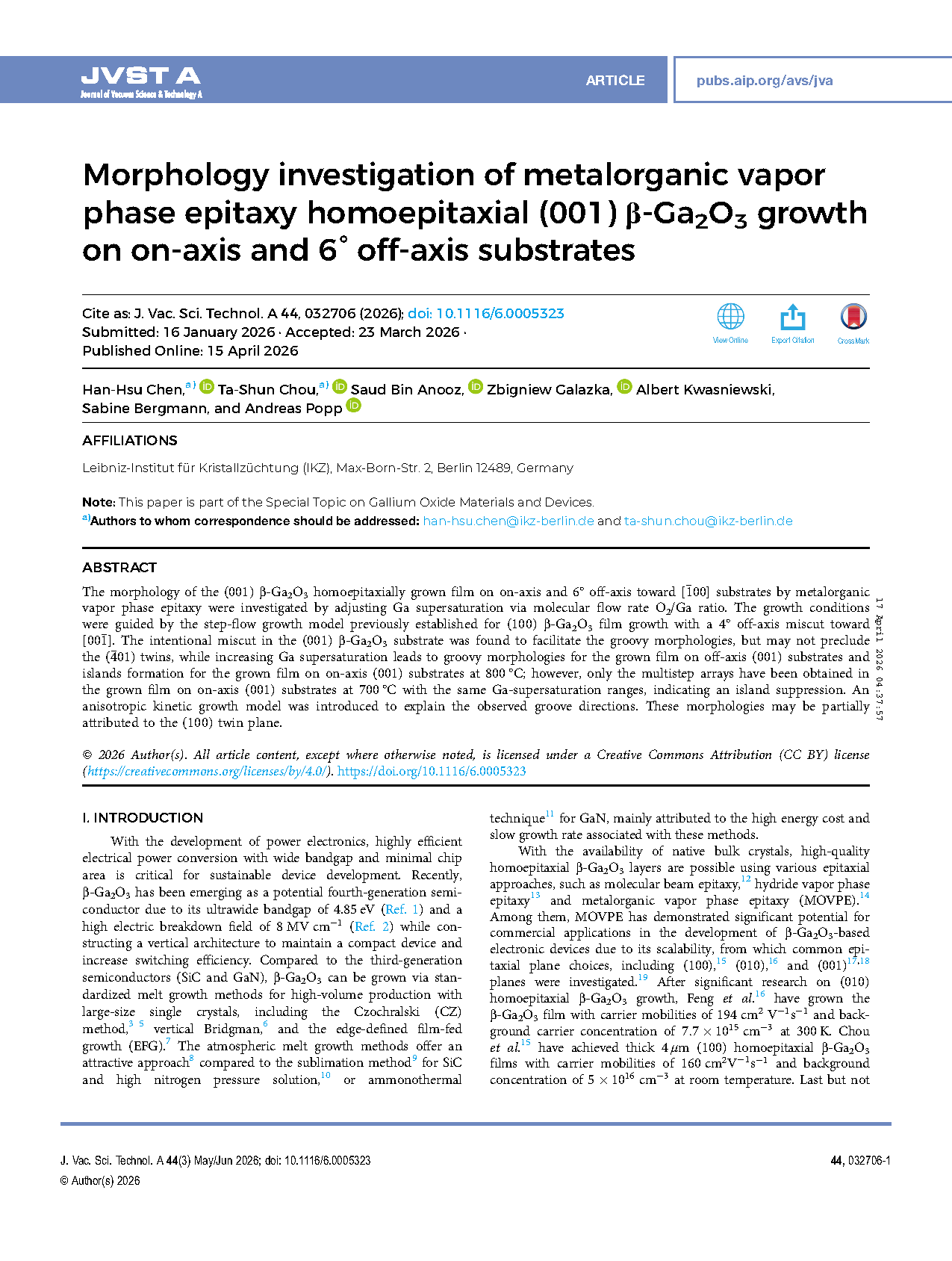
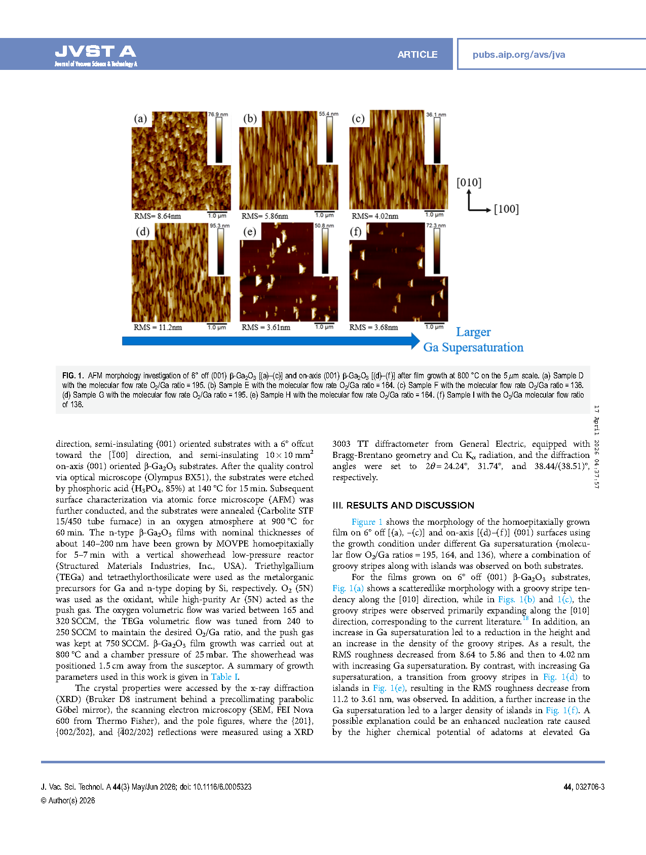
The morphology of the (001) β‑Ga₂O₃ homoepitaxially grown film on on-axis and 6° off-axis toward [-100] substrates by metalorganic vapor phase epitaxy were investigated by adjusting Ga supersaturation via molecular flow rate O₂/Ga ratio. The growth conditions were guided by the step-flow growth model previously established for (100) β‑Ga₂O₃ film growth with a 4° off-axis miscut toward [00-1]. The intentional miscut in the (001) β‑Ga₂O₃ substrate was found to facilitate the groovy morphologies, but may not preclude the (-401) twins, while increasing Ga supersaturation leads to groovy morphologies for the grown film on off-axis (001) substrates and islands formation for the grown film on on-axis (001) substrates at 800 °C; however, only the multistep arrays have been obtained in the grown film on on-axis (001) substrates at 700 °C with the same Ga-supersaturation ranges, indicating an island suppression. An anisotropic kinetic growth model was introduced to explain the observed groove directions. These morphologies may be partially attributed to the (100) twin plane.
Highlights
Investigated the surface morphology of (001) β‑Ga₂O₃ homoepitaxy on on-axis and 6° off-axis substrates toward [-100] by MOVPE.
Found that substrate miscut promotes groove morphology but cannot eliminate (-401) twins.
Observed groove formation on off-axis (001) substrates and island formation on on-axis (001) substrates at 800 °C with increased Ga supersaturation.
Suppressed island formation and obtained multistep arrays on on-axis (001) substrates by reducing growth temperature to 700 °C.
Proposed an anisotropic kinetic growth model to explain the groove orientation along [010].
Conclusion
This study applied the MOVPE growth conditions established for the step-flow growth mode of β‑Ga₂O₃ layers on (100) 4° off-oriented β‑Ga₂O₃ substrates to the homoepitaxial growth on (001) β‑Ga₂O₃ with a 6° offcut along [-100] in order to examine the surface morphology with preferential groove directions along the (010) plane. A substrate miscut in (001) β‑Ga₂O₃ was found to promote groovelike step morphologies but may not avoid (-401) twins. Under higher Ga supersaturation (molecular flow rate O₂/Ga ratio = 164, 136), these grooved morphologies formed on 6° off (001) substrates, whereas on-axis (001) substrates developed island structures at 800 °C; however, a lower growth temperature at 700 °C seemed to suppress the island formations, forming multistep arrays, implying a step-flow growth mode on the on-axis (001) substrates. An anisotropic kinetic model, incorporating surface energy and adatom mobility considerations, was proposed to explain the preferential groove directions along the (010) plane. The resulting morphologies may be attributed to the existence of (100) twin planes as well.
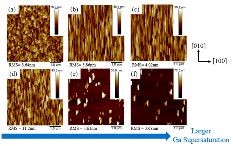
Figure 1. AFM morphology investigation of 6° off (001) β‑Ga₂O₃ [(a)–(c)] and on-axis (001) β‑Ga₂O₃ [(d)–(f)] after film growth at 800 °C on the 5 μm scale. (a) Sample D with the molecular flow rate O₂/Ga ratio = 195. (b) Sample E with the molecular flow rate O₂/Ga ratio = 164. (c) Sample F with the molecular flow rate O₂/Ga ratio = 136. (d) Sample G with the molecular flow rate O₂/Ga ratio = 195. (e) Sample H with the molecular flow rate O₂/Ga ratio = 164. (f) Sample I with the O₂/Ga molecular flow ratio of 136.
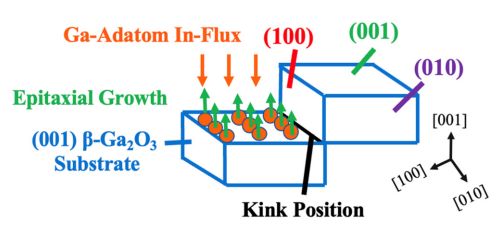
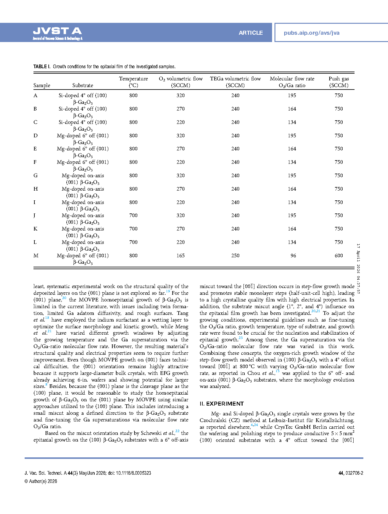
Figure 2. Illustration of the possible formation mechanism of groovy stripes and islands feature on the surface of homoepitaxially grown (001) β‑Ga₂O₃.
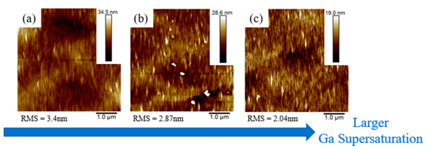
Figure 3. Morphology investigation via AFM of β‑Ga₂O₃ thin films homoepitaxially grown at 700 °C on on-axis (001) orientated substrates. (a) Sample J with the molecular flow rate O₂/Ga ratio = 195. (b) Sample K with the molecular flow rate O₂/Ga ratio = 164. (c) Sample L with the molecular flow rate O₂/Ga ratio = 136.
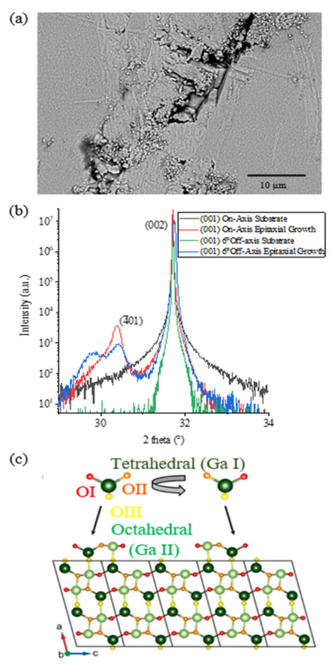
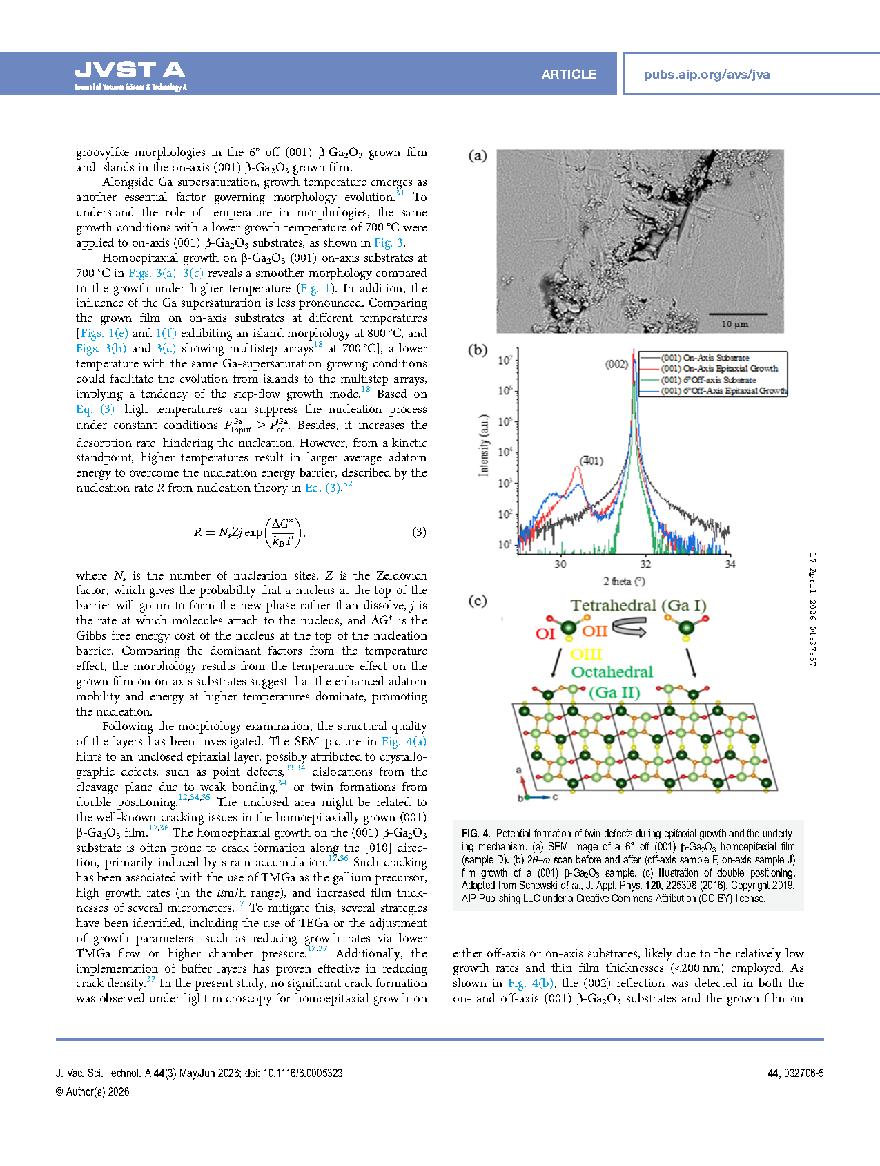
Figure 4. Potential formation of twin defects during epitaxial growth and the underlying mechanism. (a) SEM image of a 6° off (001) β‑Ga₂O₃ homoepitaxial film (sample D). (b) 2θ–ω scan before and after (off-axis sample F, on-axis sample J) film growth of a (001) β‑Ga₂O₃ sample. (c) Illustration of double positioning.
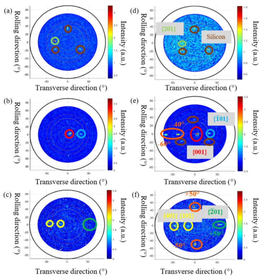
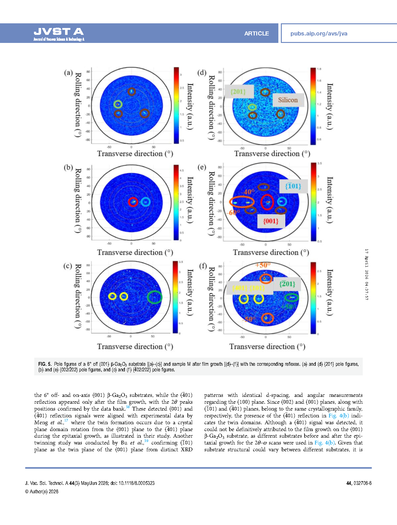
Figure 5. Pole figures of a 6° off (001) β‑Ga₂O₃ substrate [(a)–(c)] and sample M after film growth [(d)–(f)] with the corresponding reflexes. (a) and (d) {201} pole figures, (b) and (e) {002/-202} pole figures, and (c) and (f) {-402/202} pole figure
DOI:
doi.org/10.1116/6.0005323