Paper Sharing
【Member Papers】The Growth and Characterization of 6‑inch (100) β‑Ga₂O₃ Single Crystals Grown by a Casting Method
日期:2026-04-22阅读:296
Researchers from the State Key Laboratory of Silicon and Advanced Semiconductor Materials, Shangyu Institute of Semiconductor Materials, ZJU‑Hangzhou Global Scientific and Technological Innovation Center, Hangzhou Garen Semiconductor Co., Ltd. have published a dissertation titled “The Growth and Characterization of 6‑inch (100) β‑Ga₂O₃ Single Crystals Grown by a Casting Method” in Journal of Alloys and Compounds.
Background
β‑Ga₂O₃ is an ultra‑wide bandgap semiconductor with a bandgap of ~4.8 eV, featuring high critical breakdown field, intrinsic solar‑blind detection capability, and excellent physicochemical stability, making it highly promising for high‑power electronics and extreme‑environment devices. Compared with AlN and diamond, its melt growth offers advantages in cost and rate. With mature defect‑selective etching, defect density can be precisely controlled to improve device voltage resistance. Scaling β‑Ga₂O₃ wafers from 4‑inch to 6‑inch is critical for industrialization, as a 50% diameter increase expands area by 2.25× for compatibility with Si lines. However, VB tends to crack, and EFG is limited by die geometry, hindering high‑quality (100) substrates. The casting method, evolved from VGF, is seedless and mold‑free, enabling fast scaling of (100) with low stress and scalability. Based on this method, the team optimized thermal field and spontaneous crystallization, realizing the first 6‑inch (100) Sn‑doped and UID β‑Ga₂O₃ single crystals, and fabricated on‑axis and 4° off‑cut substrates with systematic characterizations.
Abstract
β‑Ga₂O₃ has emerged as a transformative ultra‑wide bandgap semiconductor (Eg ~ 4.8 eV) for high‑power and extreme‑environment electronic applications, where scaling from 4‑ to 6‑inch wafer dimensions is critical for industrial adoption. This work demonstrates a breakthrough in large‑scale β‑Ga₂O₃ crystal growth through an optimized casting method, achieving the first successful fabrication of 6‑inch 0.05 mol% (169 ppm wt) Sn‑doped wafers with both on‑axis and 4° off‑cut (100)‑oriented. Comprehensive characterization reveals excellent crystal quality with FWHM < 60 arcsec, smooth surface morphology Ra < 0.2 nm, and low defect density ≤ 4×103 cm⁻², meeting all requirements for high‑performance homoepitaxial growth. The casting method overcomes size‑limitation by controlling spontaneous crystallization while maintaining excellent reproducibility and scalability. These features address key barriers in β‑Ga₂O₃ commercialization by enabling wafer‑scale production of epitaxy and device‑ready substrates suitable for high‑performance MOSFETs and Schottky barrier diodes.
Highlights
Size Breakthrough:The casting method was adopted for the first time to successfully grow 6-inch (100) β-Ga₂O₃ single crystals, realizing the fabrication of on-axis and 4° off-cut substrates.
Excellent Crystal Quality:The full width at half maximum (FWHM) of the crystal rocking curve is < 60 arcsec, the surface roughness Ra is < 0.2 nm, and the dislocation density is ≤ 4×10³ cm⁻², which meets the requirements for epitaxy.
Significant Process Advantages:The seedless and mold-free casting method reduces structural stress and has high repeatability and industrial scalability.
Uniform Optoelectronic Performance:Sn doping achieves low resistivity and uniform carrier concentration, which is suitable for the preparation of MOSFET and SBD devices.
Conclusion
In this work, Sn doped 6‑inch β‑Ga₂O₃ single crystals were successfully grown through the casting method. The as‑grown ingot exhibited excellent quality, devoid of macroscopic defects such as stray crystals or cracks. Both on‑axis and precisely controlled 4° off‑cut (100) β‑Ga₂O₃ wafers are yielded processed, representing a significant advancement in large‑diameter wafer production. Comprehensive characterization demonstrated that both 6‑inch wafer types possess superior surface quality, thickness uniformity, and remarkable flatness, meeting the rigorous demands of high‑quality homoepitaxy growth. Electrical evaluation revealed consistently low resistivity (2×10⁻³ Ω·cm) across both entire wafers, highlighting their suitability for power device applications. Wet chemical etching analysis revealed comparable dislocation densities (4×10³ cm⁻²) and morphologies between on‑axis and off‑cut wafers, confirming the negligible influence of the 4° off‑cut on defect formation. However, Sn doping was found to increase void defect density compared to UID crystals, suggesting the need for further optimization of doping protocols during crystal growth. These findings underscore the advantages of the casting method for scalable producing of large‑diameter β‑Ga₂O₃. The high‑quality epitaxy‑ready wafers developed in this work establish a critical foundation for advancing β‑Ga₂O₃ based power electronics and optoelectronic devices toward commercial viability.
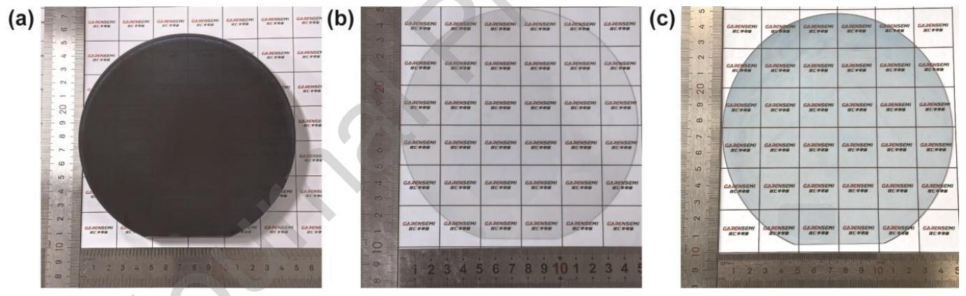
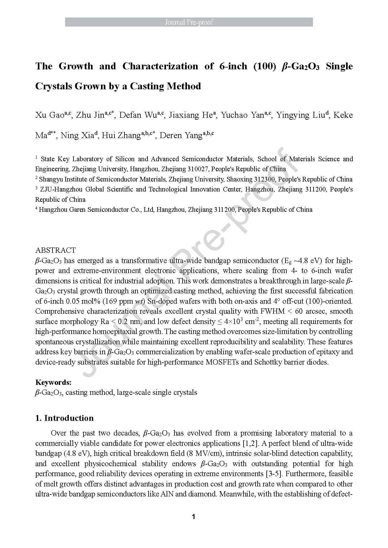
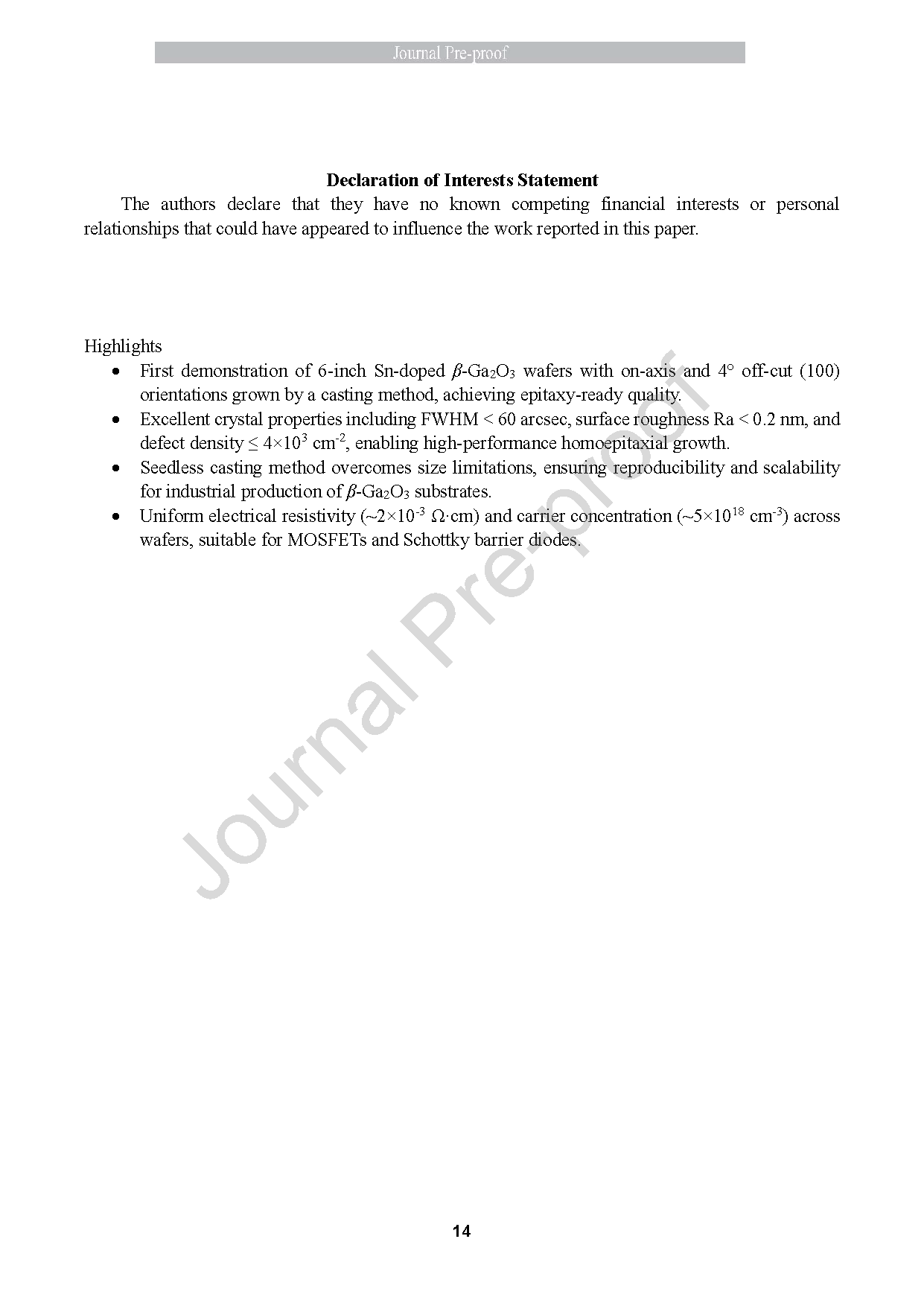
Fig.1. 6‑inch diameter β‑Ga₂O₃ of (a) ingot grown by a casting method, (b) on‑axis and (c) 4° off‑cut (100) mirror‑polished wafer.
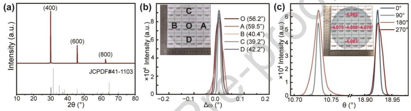
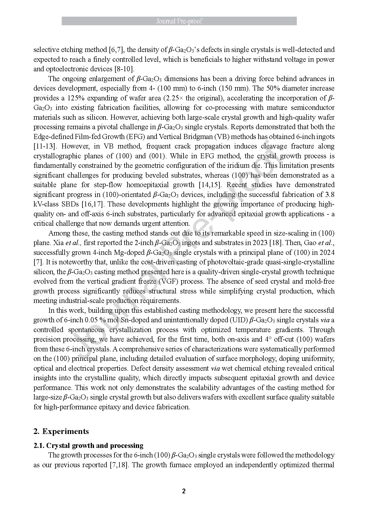
Fig. 2. (a) HRXRD patterns of Sn‑doped β‑Ga₂O₃ crystals, (b) X‑ray rocking curves (ω‑scan) of the (400) reflection for the Sn‑doped 6‑inch on‑axis (100) wafer, and (c) HRXRD θ‑2θ scan at the point O in four different in‑plane directions (Φ) separated by 90° of the 4° off‑cut (100) wafer.
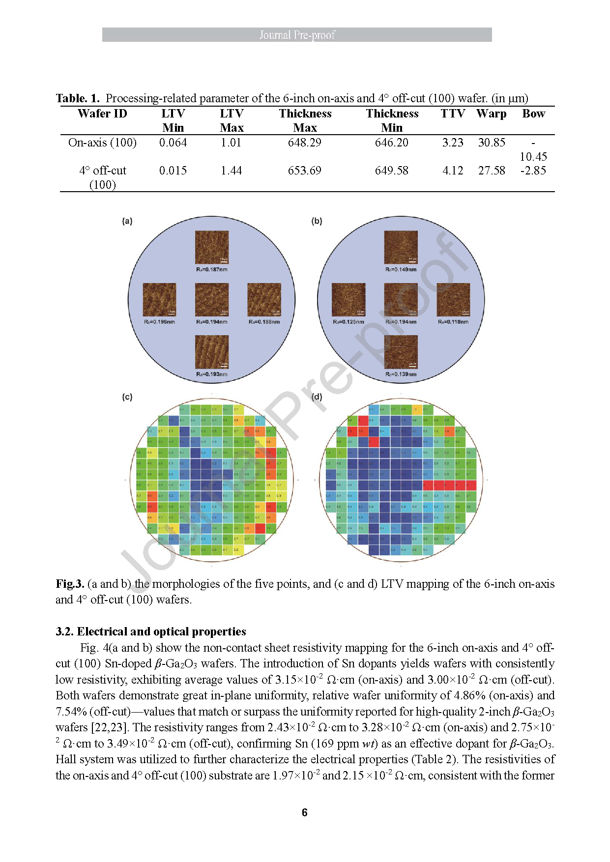
Fig.3. (a and b) the morphologies of the five points, and (c and d) LTV mapping of the 6‑inch on‑axis and 4° off‑cut (100) wafers.
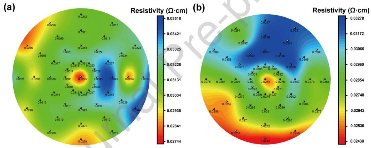
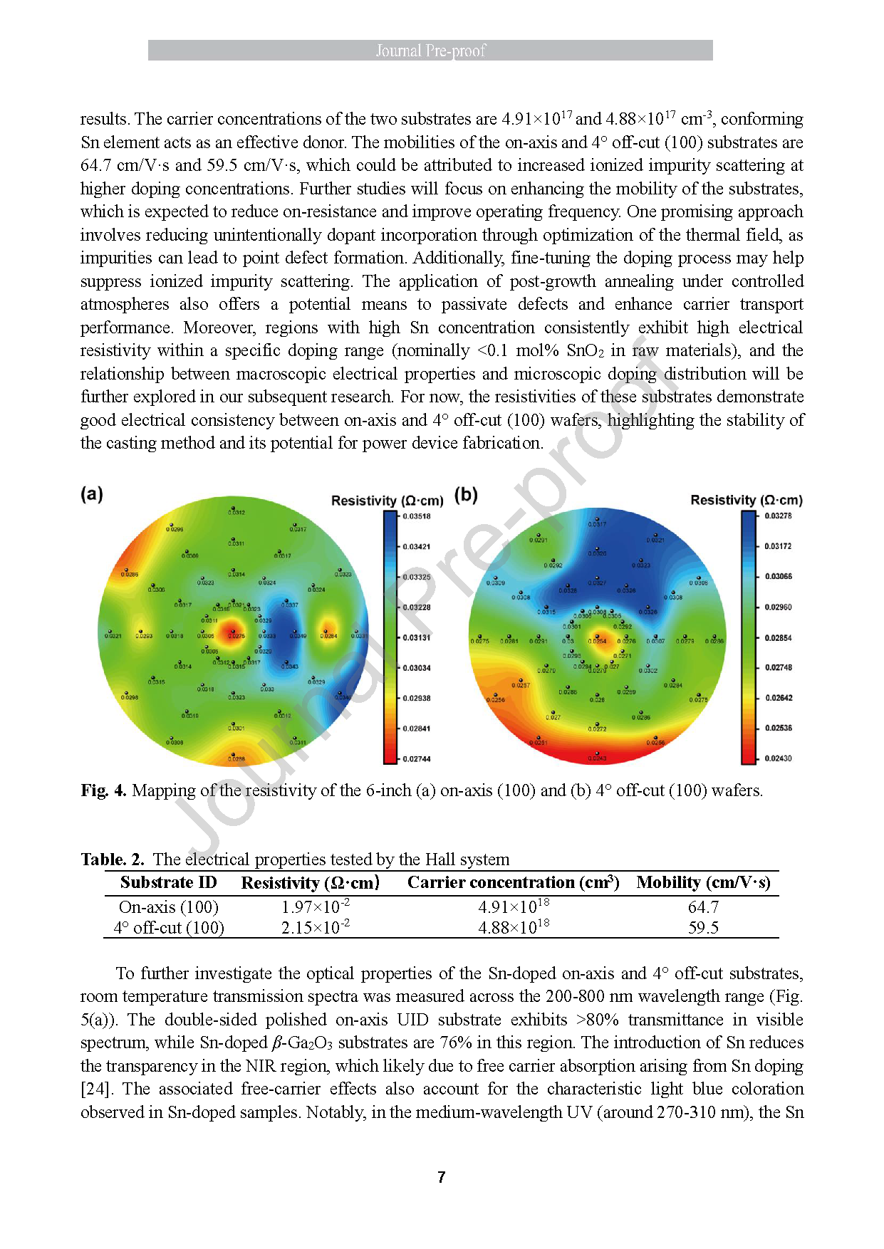
Fig. 4. Mapping of the resistivity of the 6‑inch (a) on‑axis (100) and (b) 4° off‑cut (100) wafers.
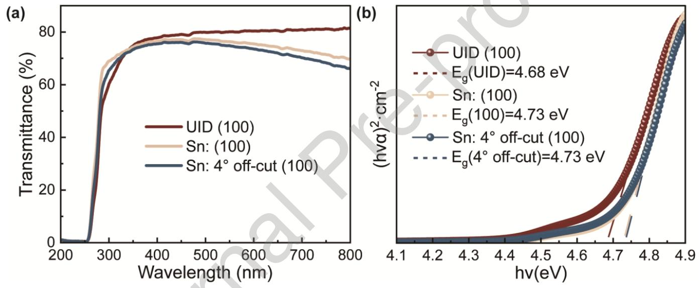
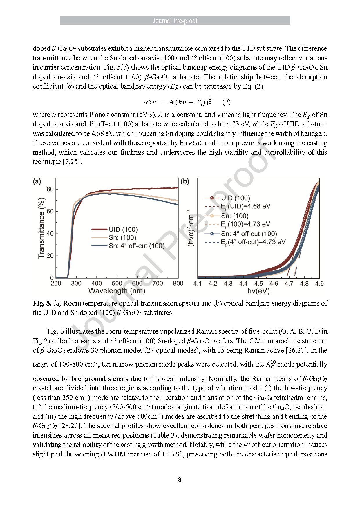
Fig. 5. (a) Room temperature optical transmission spectra and (b) optical bandgap energy diagrams of the UID and Sn doped (100) β‑Ga₂O₃ substrates.
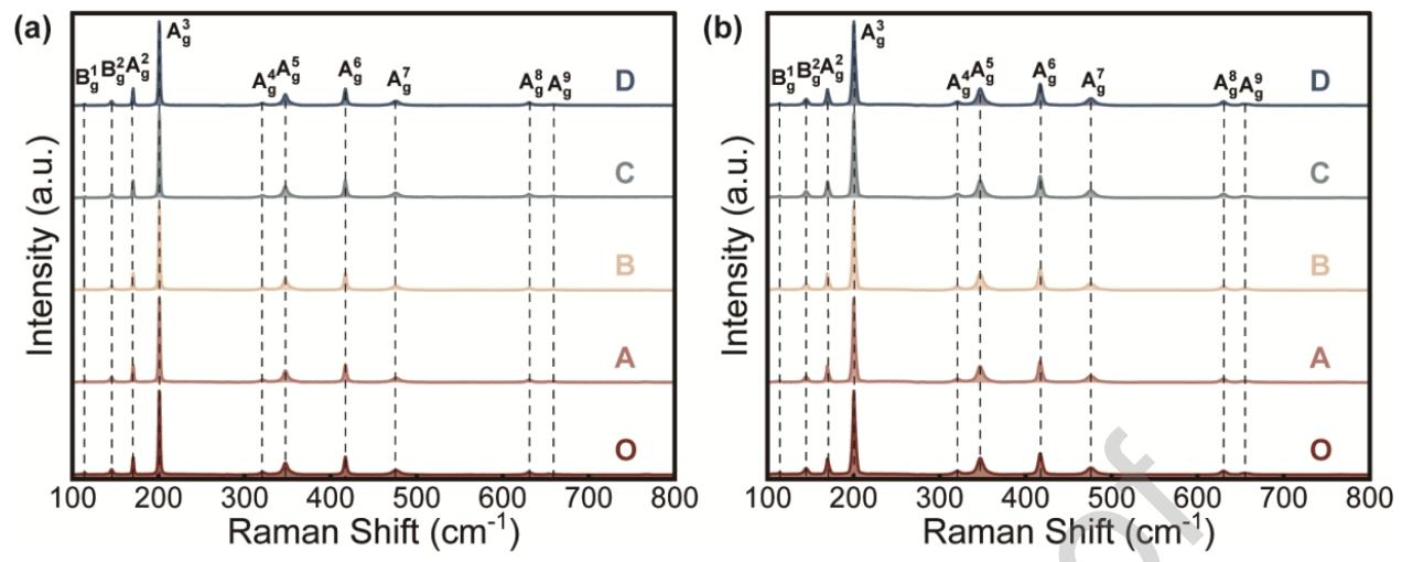
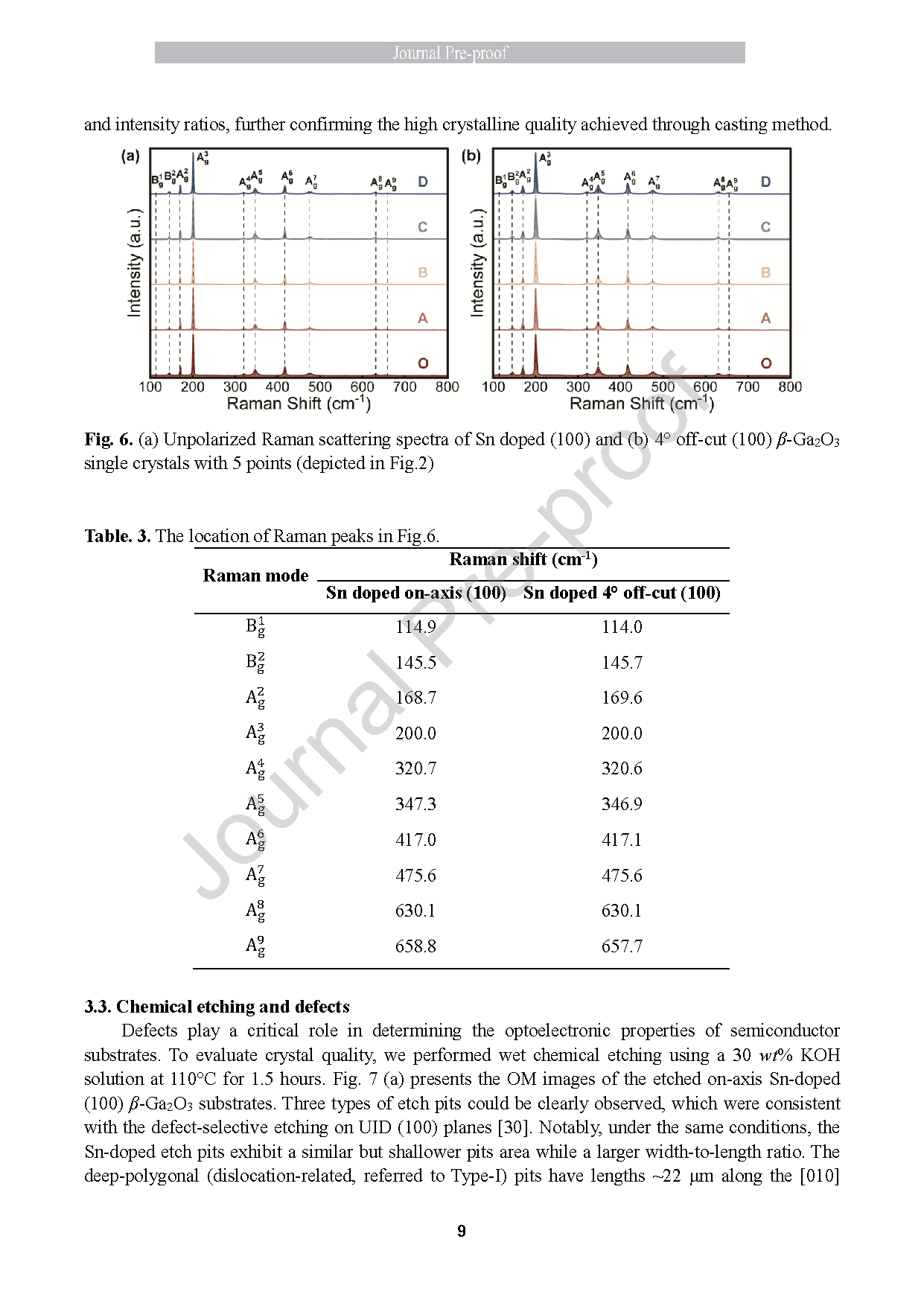
Fig. 6. (a) Unpolarized Raman scattering spectra of Sn doped (100) and (b) 4° off‑cut (100) β‑Ga₂O₃ single crystals with 5 points (depicted in Fig.2).
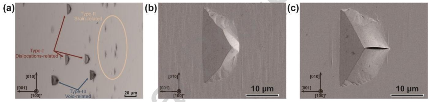
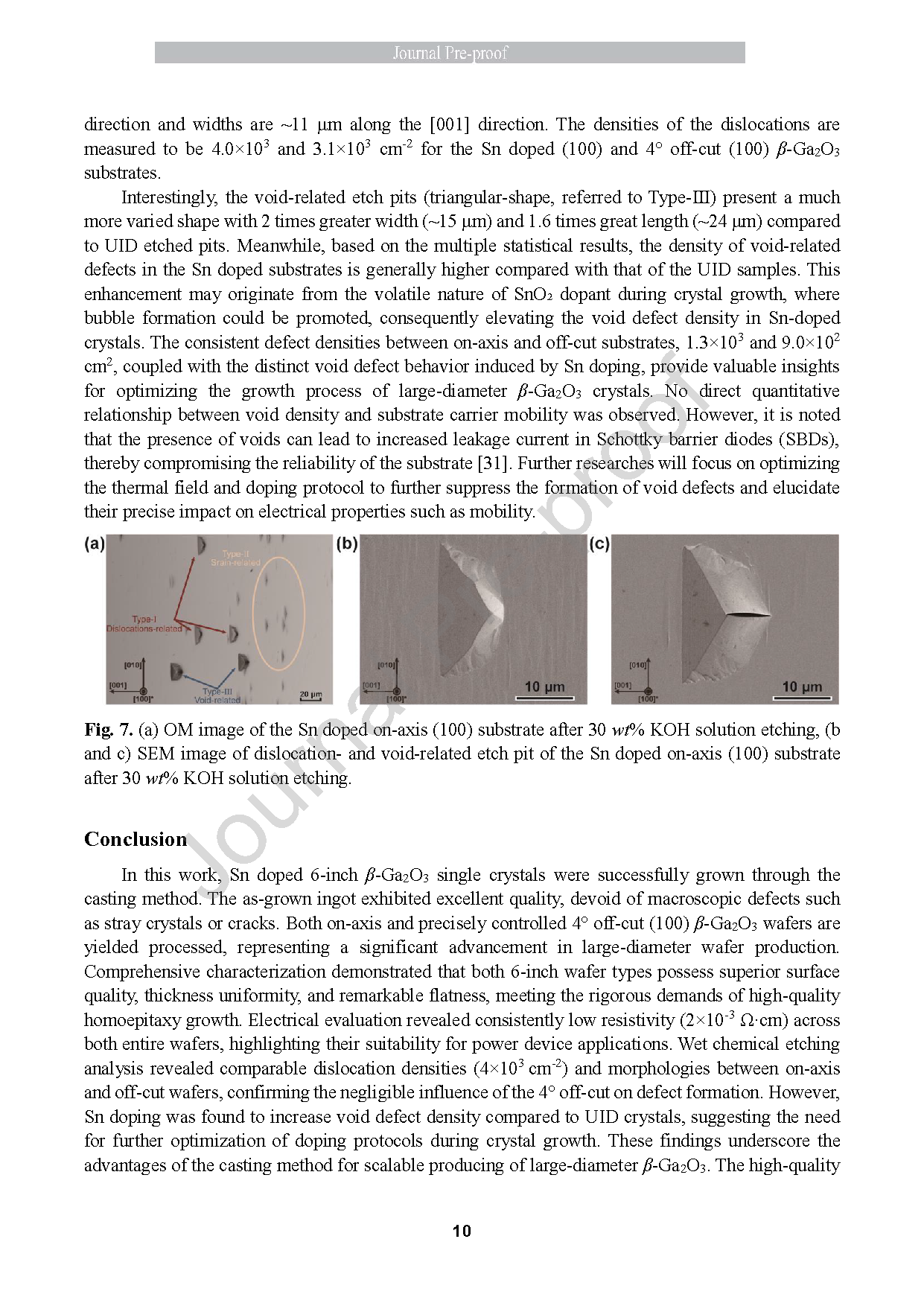
Fig. 7. (a) OM image of the Sn doped on‑axis (100) substrate after 30 wt% KOH solution etching, (b and c) SEM image of dislocation‑ and void‑related etch pit of the Sn doped on‑axis (100) substrate after 30 wt% KOH solution etching.
DOI:
doi.org/10.1016/j.jallcom.2026.187699