Paper Sharing
【International Papers】High-yield fabrication of high-performance β-Ga₂O₃ MOSFETs on a (010) 2″ substrate
日期:2026-04-23阅读:197
Researchers from the Air Force Research Laboratory, Cornell University, and KBR, Inc. have published a dissertation titled "High-yield fabrication of high-performance β-Ga₂O₃ MOSFETs on a (010) 2″ substrate" in APL Electronic Devices.
Background
β-Ga₂O₃ is an ultra-wide bandgap (UWBG) semiconductor with a bandgap of 4.8 eV, high critical electric field strength, and a Baliga’s figure of merit far exceeding GaN and SiC. It has two key advantages: shallow n-type dopants and large-area native substrates, with melt-grown wafers scaled to 6 inches commercially. Lateral β-Ga₂O₃ MOSFETs are promising for RF and power switching, but prior 2″ demonstrations focused on single-device performance rather than aggregate yield and performance, and used (−201) substrates incompatible with fast epitaxy. This work fabricates devices on 2″ (010) substrates to validate scalable manufacturing.
Abstract
We have fabricated lateral β-Ga₂O₃ MOSFETs on a 2″ (010) substrate with peripheries ranging from 100 μm to 2 mm and an overall yield of 84.5% (over 95% excluding edge dies). Devices featured source–drain spacings of 1, 2, and 5 μm with regrown ohmic contacts and scaled T-gates. 1 μm devices had Ron as low as 24 Ω·mm and 5 μm devices showed Vbk as high as 863 V. Average fT and fmax for 1, 2 and 5 μm devices were 7 ± 2, 6 ± 1, and 3.7 ± 0.7 and 22 ± 4, 17 ± 3, and 9 ± 0.9 GHz, respectively. Under large-signal operation, a 2 mm-periphery, 2 μm device demonstrated a Pout value of 467 mW (26.7 dB) at 5 GHz, the highest reported net RF power for a Ga₂O₃ transistor. Aggregate device performance was analyzed and sources of device failure and performance degradation were identified, including short-channel effects and gate leakage. These results demonstrate the viability of β-Ga₂O₃ MOSFET fabrication on large-area substrates and provide insight into technical barriers in manufacturability.
Highlights
First high-yield fabrication of high-performance β-Ga₂O₃ MOSFETs on 2″ (010) substrates, with 84.5% overall yield and >95% yield excluding edge dies.
5 μm devices reach 863 V breakdown voltage with power figure of merit comparable to commercial SiC; 1 μm devices have R_on as low as 24 Ω·mm.
Achieve the highest reported net RF power for Ga₂O₃ transistors: 467 mW at 5 GHz for a 2 mm-periphery device.
Systematically identify manufacturing limits: gate leakage, air-bridge plating failure, and parasitic Si channel at the substrate-epitaxy interface.
Conclusion
β-Ga₂O₃ MOSFETs were successfully fabricated on a 2″ (010) wafer, including regrown Ohmic contacts, with high yield and good performance metrics. Device performance was shown to be in-class with other state-of-the-art transistors; the best devices had a Baliga’s figure of merit in class with previously published devices and higher than the Si unipolar limit. Device performance was analyzed individually and collectively. Failure mechanisms included poor channel modulation, gate leakage, electroplating failure, and parasitic Si at the substrate–epitaxy interface; possible mitigations were proposed. These results provide a snapshot of the current state of manufacturability of lateral β-Ga₂O₃ MOSFETs and highlight paths toward the continued improvement of materials, processes, and devices in the β-Ga₂O₃ system.
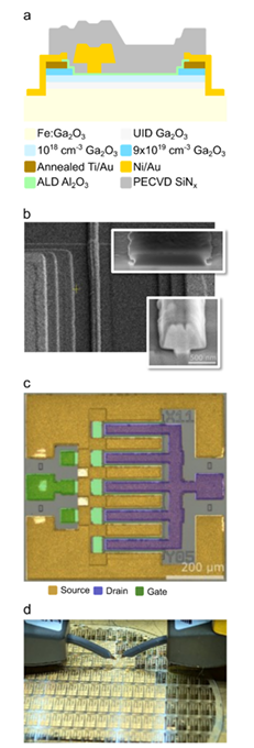
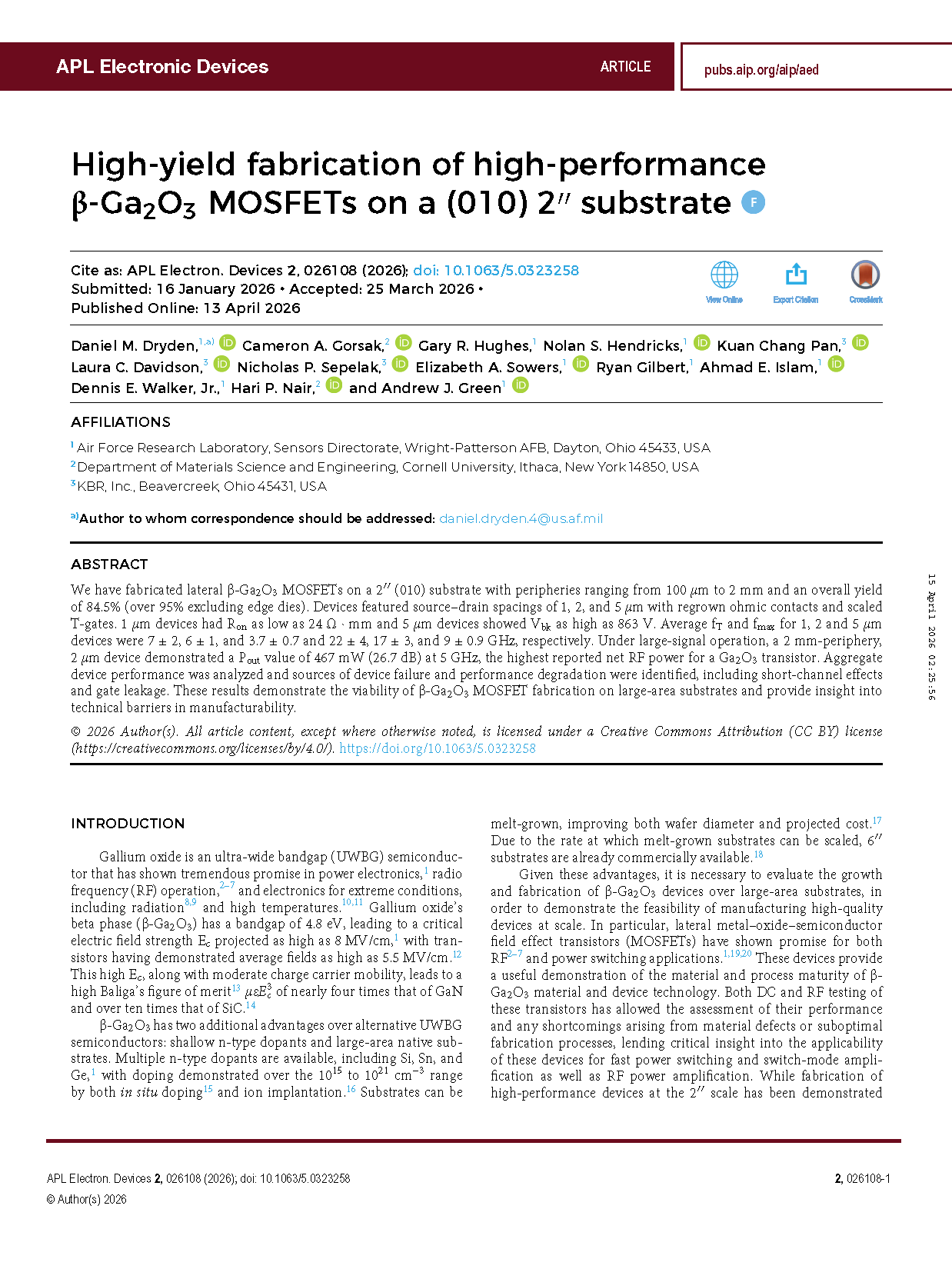
Figure 1 (a) Cross-sectional schematic of the MOSFETs. (b) SEM micrograph of the device active channel; top inset: the regrowth mask after β-Ga₂O₃ regrowth but before liftoff; bottom inset: cross section of the T-gate. (c) Colorized SEM of a 10 × 200 μm air-bridged device. (d) The 2″ wafer on the RF test bench.
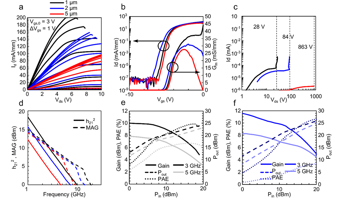
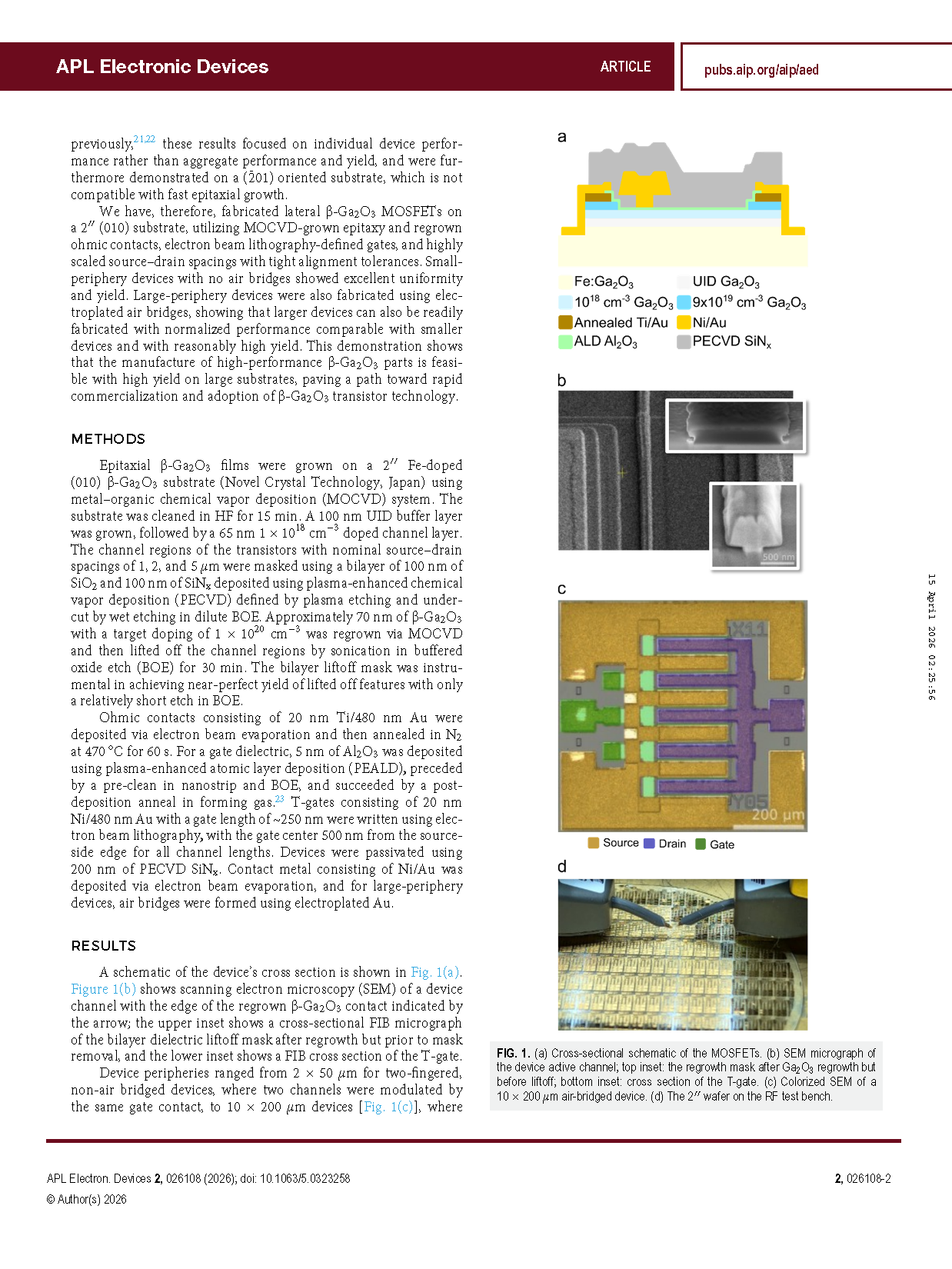
Figure 2 Individual device results for the 1 μm (black), 2 μm (blue), and 5 μm (red) source–drain devices: (a) family of curves, (b) transfer curves, (c) off-state breakdown, (d) forward current gain h₂₁, (e) load-pull of the 1 μm LSD device, and (f) load-pull of the 2 μm LSD device.
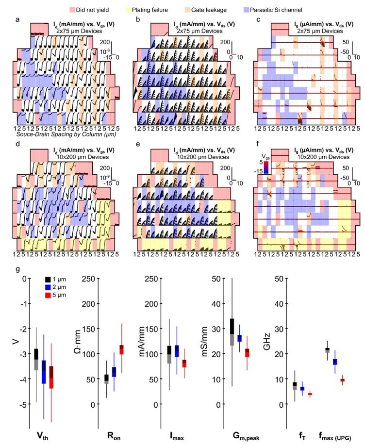
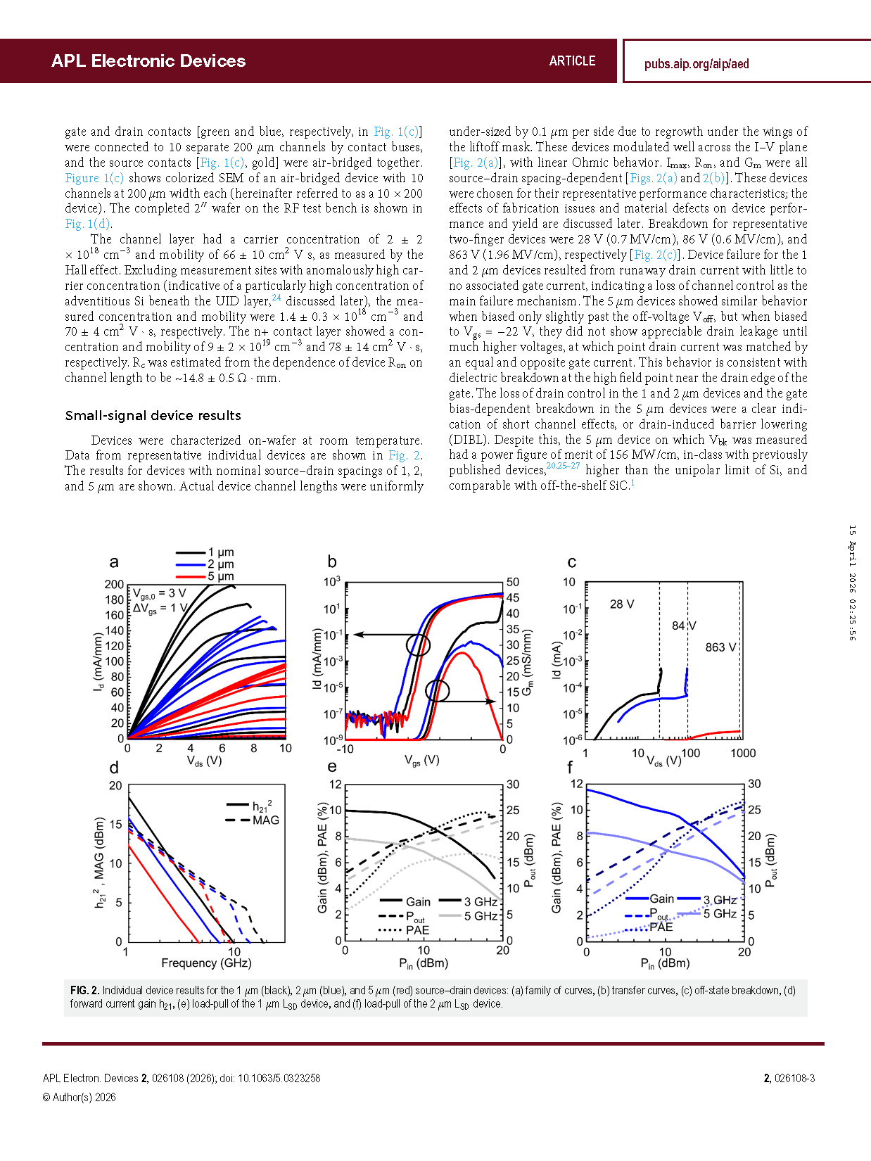
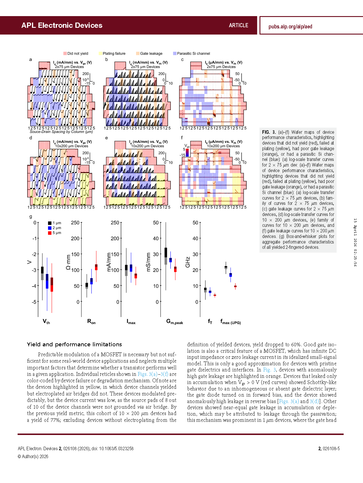
Figure 3 (a)–(f) Wafer maps of device performance characteristics, highlighting devices that did not yield (red), failed at plating (yellow), had poor gate leakage (orange), or had a parasitic Si channel (blue): (a) log-scale transfer curves for 2 × 75 μm devices, (b) family of curves for 2 × 75 μm devices, (c) gate leakage curves for 2 × 75 μm devices, (d) log-scale transfer curves for 10 × 200 μm devices, (e) family of curves for 10 × 200 μm devices, and (f) gate leakage curves for 10 × 200 μm devices. (g) Box-and-whisker plots for aggregate performance characteristics of all yielded two-fingered devices.
DOI:
doi.org/10.1063/5.0323258