Paper Sharing
【Domestic Papers】High-performance solar-blind ultraviolet photodetector based on β-Ga₂O₃/SnO₂ heterojunction and its corona discharge detection performance
日期:2026-04-23阅读:198
Researchers from the Chongqing University of Technology, Changchun University of Science and Technology, and Chongqing Institute of Green and Intelligent Technology, Chinese Academy of Sciences have published a dissertation titled "High-performance solar-blind ultraviolet photodetector based on β‑Ga₂O₃/SnO₂ heterojunction and its corona discharge detection performance" in Journal of Alloys and Compounds.
Background
Solar‑blind ultraviolet photodetectors (SBUV‑PDs) have advantages of high sensitivity, low noise and strong anti‑interference ability, showing great application potential in missile identification and tracking, space communication, environmental monitoring and corona detection. Traditional SBUV‑PDs based on narrow‑bandgap semiconductors suffer from performance degradation at high temperatures and requirement of optical filters, leading to high dark current, slow response and poor high‑temperature performance. β‑Ga₂O₃ is an ideal material for high‑performance SBUV‑PDs due to its ultra‑wide bandgap, excellent crystal stability and high absorption coefficient in the solar‑blind band. However, p‑type doping of β‑Ga₂O₃ is difficult, making it challenging to fabricate homojunction devices. Therefore, heterojunctions are usually constructed with wide‑bandgap semiconductors such as GaN, ZnO and SnO₂. SnO₂ has a wide bandgap, high room‑temperature electron mobility and low carrier recombination rate, and exhibits good lattice matching with β‑Ga₂O₃, which can suppress interface defects and improve device photoelectric performance.
Abstract
β‑Ga₂O₃, with its ultra‑wide bandgap, is an ideal material for solar‑blind ultraviolet photodetectors (SBUV‑PDs). In this work, high‑quality β‑Ga₂O₃ thin films were prepared via the mist‑assisted chemical vapor deposition (Mist‑CVD) method, a cost‑effective and non‑vacuum method. Under 245 nm light irradiation, the β‑Ga₂O₃/SnO₂ PD exhibits excellent photoelectric response and detection performance, including a responsivity (R) of 53.22 A/W, a photo‑to‑dark current ratio (PDCR) of 1.28 × 10⁶, and a specific detectivity (D*) of 2.43 × 10¹³ Jones. The detection capability of the heterojunction SBUV‑PD for weak deep‑ultraviolet signals (NEP of 3.92 ×10⁻¹⁵ W/Hz¹ᐟ²) is significantly superior to that of the reported heterojunction SBUV‑PDs. These superior characteristics are attributed to the low oxygen vacancy defect density and high film crystallinity, which reduces the carrier recombination. Furthermore, the type‑I band alignment formed between β‑Ga₂O₃ and SnO₂ enables efficient separation of photogenerated electron‑hole pairs under bias voltage, significantly improving carrier migration. Simultaneously, the theoretical simulation of Crosslight APSYS is used to clarify the physical mechanism of the device. Additionally, in a corona discharge simulation experiment, the detector can effectively detect extremely weak SBUV signals (~11 nW/cm²). This study combines experiments and simulations, which is expected to promote further exploration of high‑performance β‑Ga₂O₃ SBUV‑PDs.
Highlights
Low‑cost and non‑vacuum Mist‑CVD method is adopted to fabricate β‑Ga₂O₃/SnO₂ heterojunction solar‑blind UV photodetectors with high crystallinity and low oxygen vacancy defect density.
The device achieves high responsivity of 53.22 A/W, high specific detectivity of 2.43×10¹³ Jones, and ultra‑low NEP of 3.92×10⁻¹⁵ W/Hz¹ᐟ², showing better comprehensive performance than most reported heterojunction devices.
The β‑Ga₂O₃/SnO₂ heterojunction is confirmed to be type‑I band alignment, and the built‑in electric field efficiently separates photogenerated carriers; the working mechanism is revealed by theoretical simulation.
The detector successfully detects weak corona discharge signals down to 11 nW/cm², showing promising application in high‑voltage power equipment monitoring.
Conclusion
In summary, we have successfully fabricated high‑performance β‑Ga₂O₃/SnO₂ heterojunction SBUV‑PD using a cost‑effective Mist‑CVD process. The heterojunction device demonstrated significantly enhanced photoelectric performance compared to a β‑Ga₂O₃ PD, exhibiting a R of 53.22 A/W, a D* of 2.43 × 10¹³ Jones, and an EQE of 2.70 × 10⁴%. The NEP was also significantly reduced, reaching 3.92 × 10⁻¹⁵ W/Hz¹ᐟ², demonstrating the device’s ability to detect extremely weak signals. Furthermore, the theoretical simulations provided valuable insights into the device’s underlying physical mechanisms, which were consistent with the experimental results. Finally, the heterojunction PD was successfully integrated into a simulated high‑voltage corona discharge detection system, where it could detect SBUV signals as low as 11 nW/cm². These results demonstrate the potential of our work to facilitate the fabrication of high‑performance, low‑cost SBUV‑PDs with practical applications for high‑sensitivity corona detection.
Project Support
This work was financially supported by the National Natural Science Foundation of China (51574054), Chongqing Science and Technology Bureau (CSTB2025TIAD‑STX0017), Joint Fund of Chongqing Municipal Education Commission and Science and Technology Bureau (CSTB2025NSCQ‑LZX0071, CSTB2024NSCQ‑LZX0022), Chongqing University of Technology (gzIcx20243305).
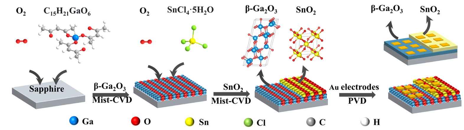
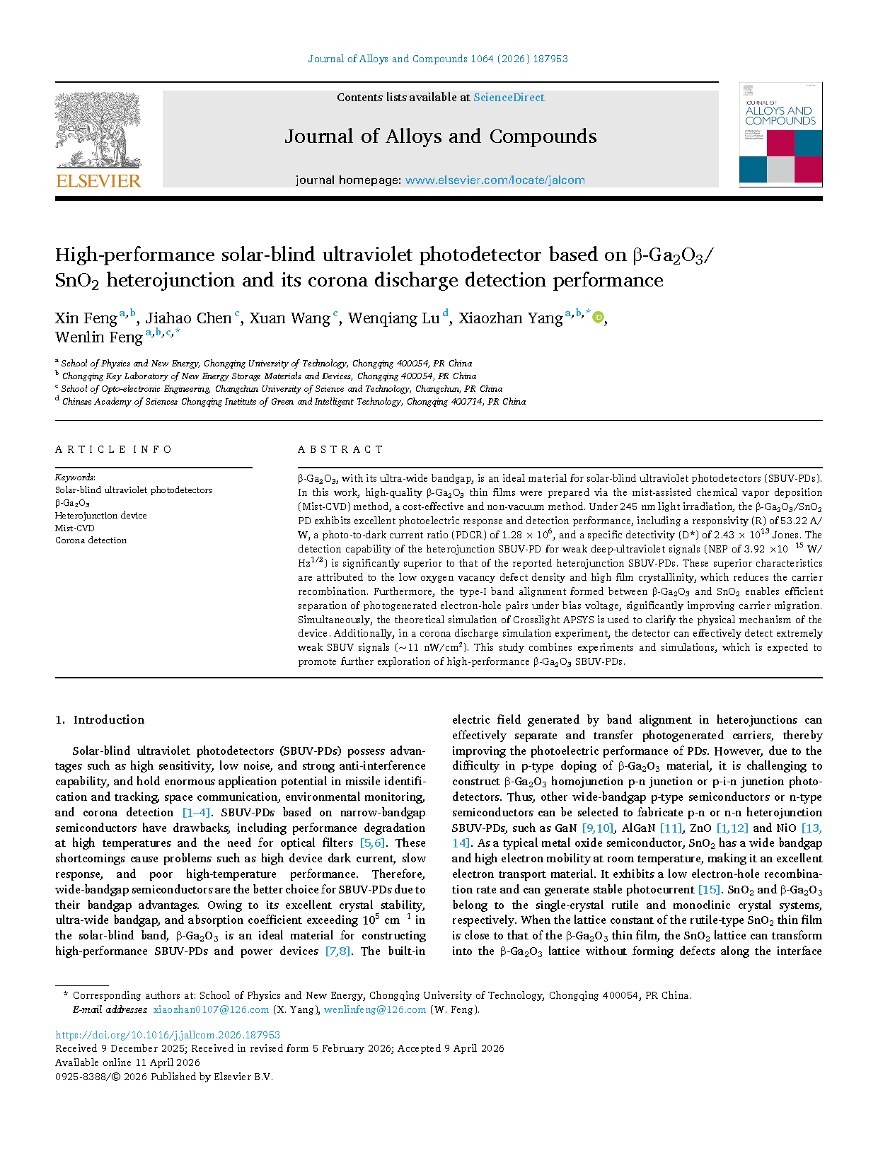
Figure 1 Preparation process of the thin film and fabrication process of the device.
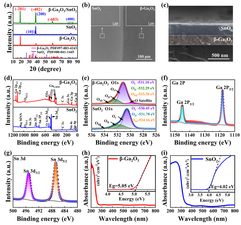
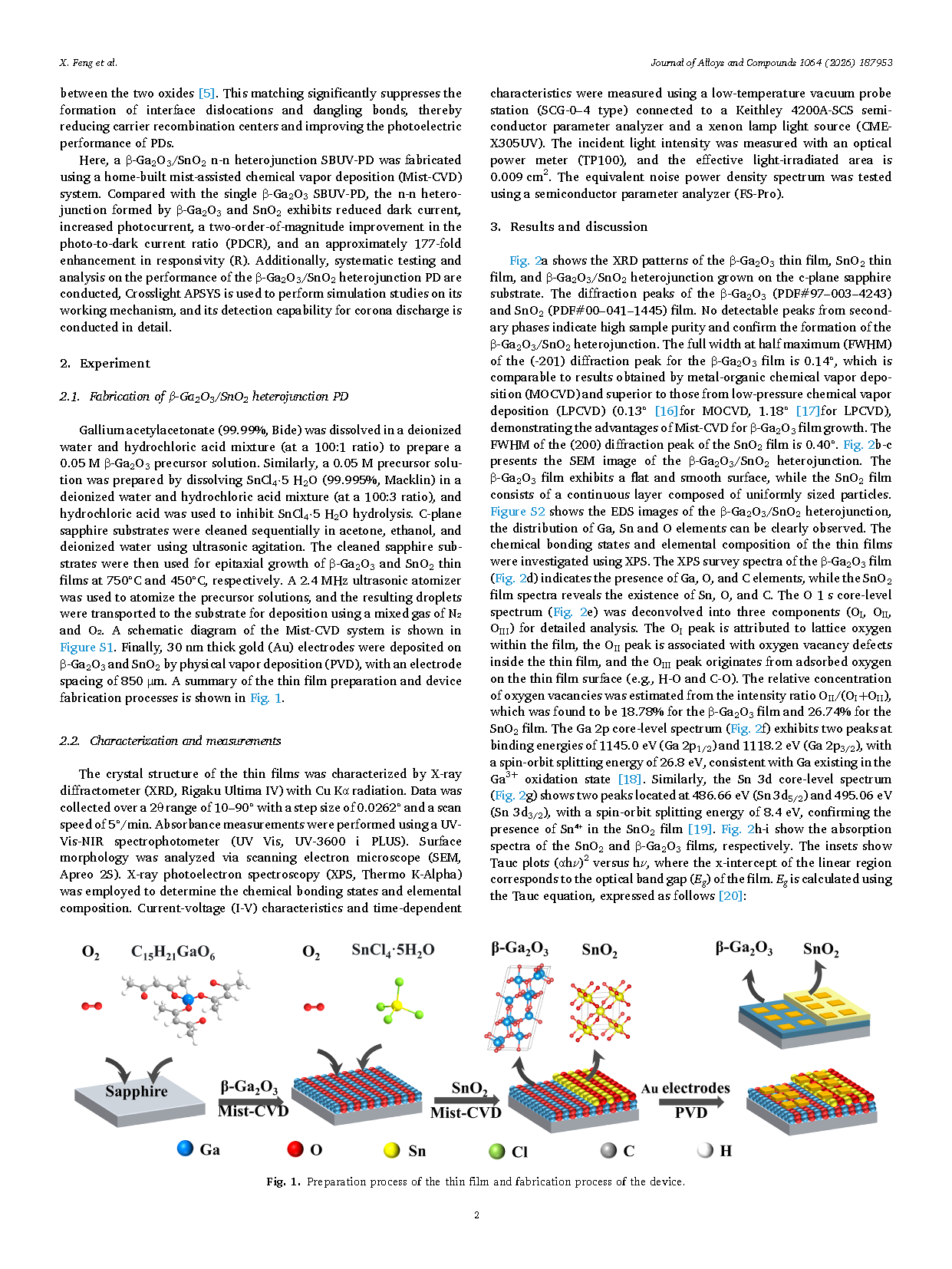
Figure 2 (a) XRD patterns of β-Ga₂O₃, SnO₂, and β-Ga₂O₃/SnO₂ heterojunction. (b) Top-view SEM images of the SnO₂ and β-Ga₂O₃ thin films. (c) Cross-sectional SEM images of β-Ga₂O₃/SnO₂ heterojunction. XPS spectra (d) Survey spectrum of β-Ga₂O₃ and SnO₂, (e) O 1s spectra of β-Ga₂O₃ and SnO₂, (f) Ga 2p spectrum, (g) Sn 3d spectrum. UV-Vis absorption spectra of (h) β-Ga₂O₃ thin film, (i) SnO₂ thin film, the inset in each spectrum shows the plot of (αhν)² versus hν.
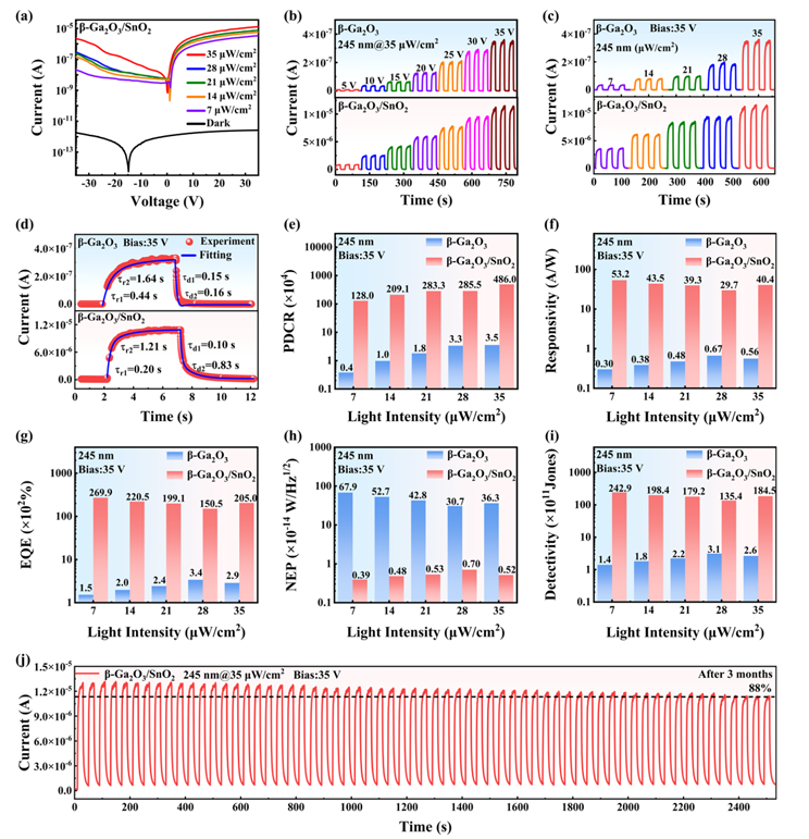
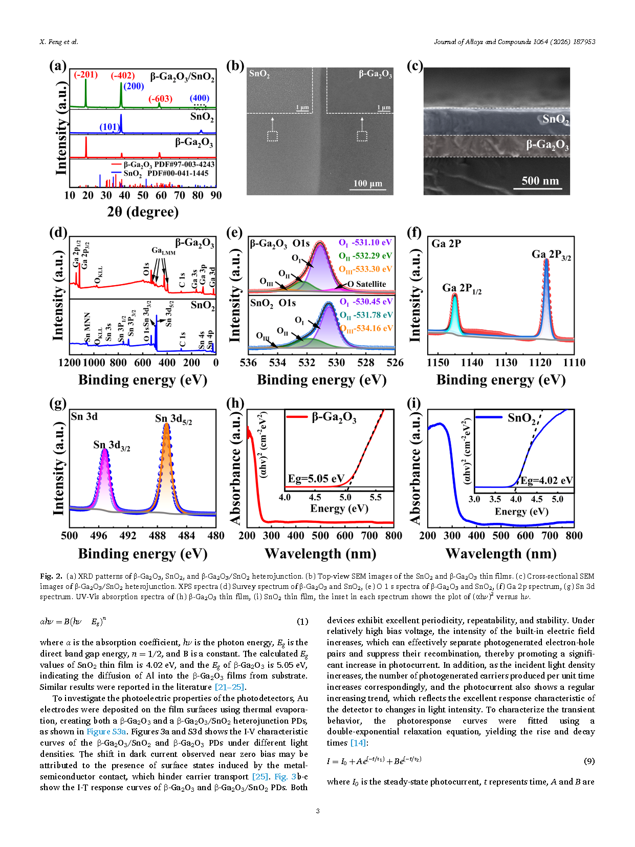
Figure 3 (a) I-V curves under different light intensities. (b) I-T curves under different bias voltages. (c) I-T curves under different light intensities. (d) Experimental and fitted curves of current rise and decay processes at a bias voltage of 35 V. Under different light intensities (e) PDCR, (f) R, (g) EQE, (h) NEP, (i) D*. (j) Long-term stability test.
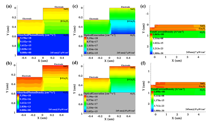
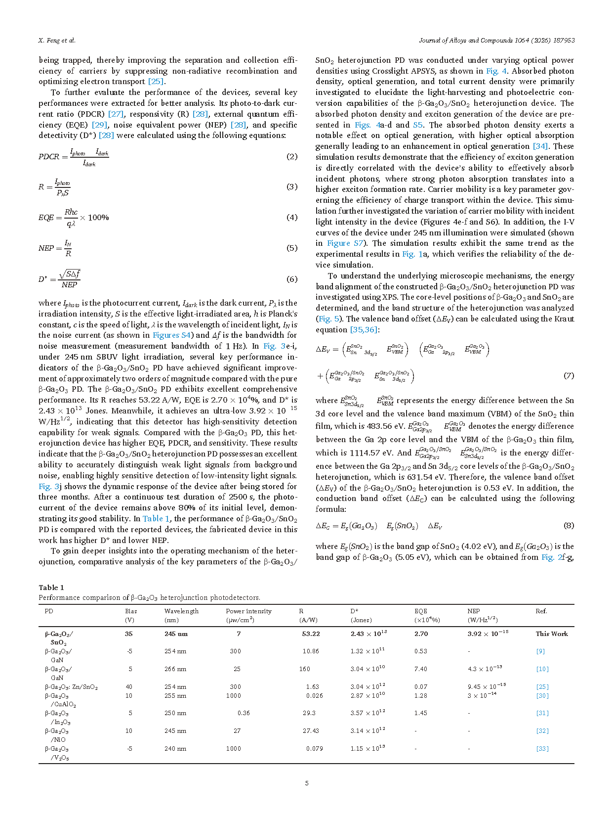
Figure 4 Theoretical simulation of β-Ga₂O₃/SnO₂ PD under 245 nm illumination with different optical power densities. Absorbed photon density (a) 7 μW/cm², (b) 35 μW/cm². Optical generation (c) 7 μW/cm² (d) 35 μW/cm². Total current density (e) 7 μW/cm², (f) 35 μW/cm²
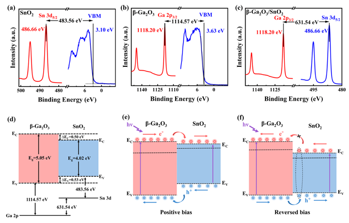
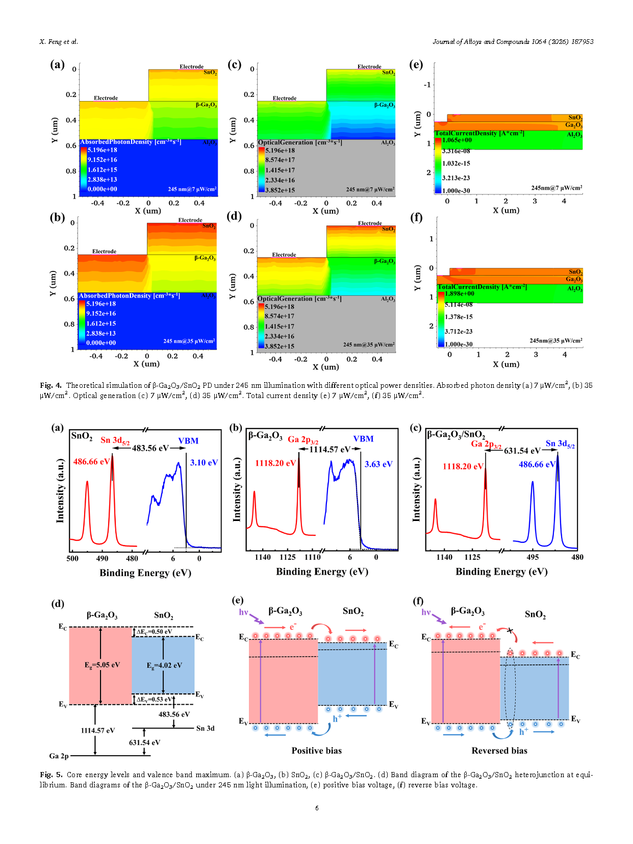
Figure 5 Core energy levels and valence band maximum. (a) β-Ga₂O₃ (b) SnO₂ (c) β-Ga₂O₃/SnO₂. (d) Band diagram of the β-Ga₂O₃/SnO₂ heterojunction at equilibrium. Band diagrams of the β-Ga₂O₃/SnO₂ under 245 nm light illumination, (e) positive bias voltage, (f) reverse bias voltage.
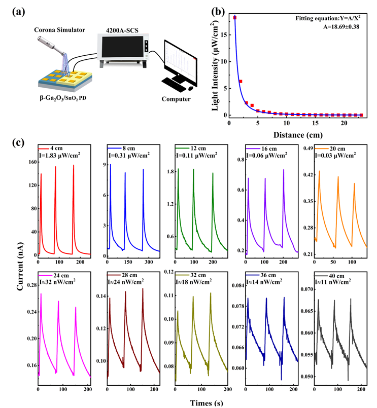
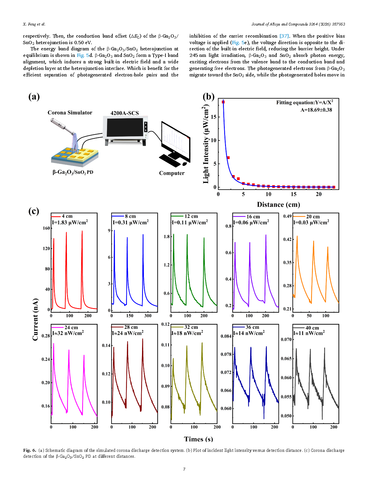
Figure 6 (a) Schematic diagram of the simulated corona discharge detection system. (b) Plot of incident light intensity versus detection distance. (c) Corona discharge detection of the β-Ga₂O₃/SnO₂ PD at different distances.
DOI:
doi.org/10.1016/j.jallcom.2026.187953