Paper Sharing
【Member Papers】A β-Ga₂O₃ DUV/X-ray detector with high sensitivity and rapid response fabricated by Mist-CVD
日期:2026-04-23阅读:234
Background and Work Overview
Precise detection of high-energy photons plays an irreplaceable role in frontier applications such as deep-space exploration, medical CT diagnostics, and industrial nondestructive testing. However, mainstream commercial semiconductor detectors still face critical challenges, including complex fabrication processes, heavy reliance on expensive vacuum equipment, and limited stability under extreme conditions.
To reduce manufacturing costs while breaking through existing performance limits, the research team led by Prof. Hao Yue from Xidian University proposed a highly promising and industrially viable approach. By adopting a cost-effective and environmentally tolerant mist chemical vapor deposition (Mist-CVD) technique, the team successfully “grew” high-crystallinity gallium oxide thin films on sapphire substrates.
Based on these films, a dual-mode deep-ultraviolet (DUV) and X-ray photodetector was fabricated. The device not only leverages intrinsic defect physics to achieve substantial photoconductive gain, effectively balancing the long-standing trade-off between high sensitivity and fast response, but also demonstrates unprecedented detection sensitivity and baseline stability under extremely weak X-ray irradiation.
This work opens a new pathway toward next-generation low-cost, radiation-resistant optoelectronic devices. The results, titled “A β-Ga₂O₃ DUV/X-ray detector with high sensitivity and rapid response fabricated by Mist-CVD”, were recently published in the journal Chinese Journal of Electronics.
Breaking Dependence on Expensive Vacuum Systems: High-Quality Films via Low-Cost Processing
In conventional epitaxial growth of ultra-wide bandgap semiconductors, processes typically rely on ultra-high vacuum environments and costly deposition systems, creating significant barriers to commercialization.
The key innovation of this work lies in the introduction of Mist-CVD, a low-cost and highly tolerant technique. By precisely controlling parameters such as precursor solution concentration and carrier gas flow under atmospheric pressure, the team successfully guided the microscopic crystallization process.
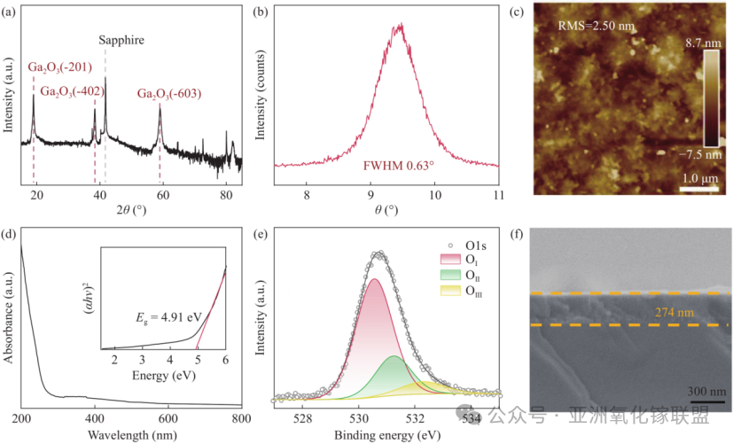
Characterization results confirm that the resulting Ga₂O₃ thin films are free from secondary phases, exhibit controllable oxygen vacancy concentrations, and possess dense and smooth surface morphologies comparable to those achieved by state-of-the-art vacuum-based methods.
This process advancement significantly reduces carrier scattering at the electrode interface, providing a solid material foundation for achieving ultralow dark current in high-performance detectors.
Engineering Defect Dynamics: Achieving High Gain and Fast Response in the DUV Region
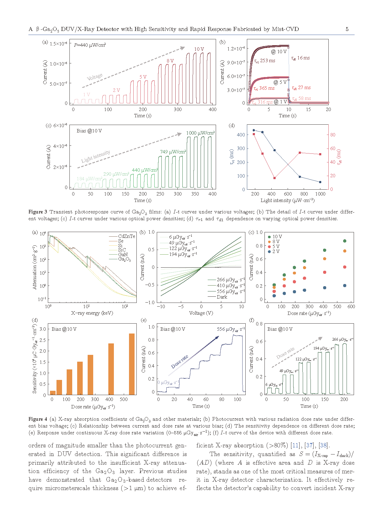
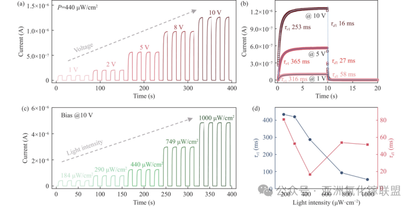
In photodetectors, “high sensitivity” and “fast response” are typically contradictory: high gain often relies on long carrier trapping times, which inevitably lead to slow recovery (persistent photoconductivity).
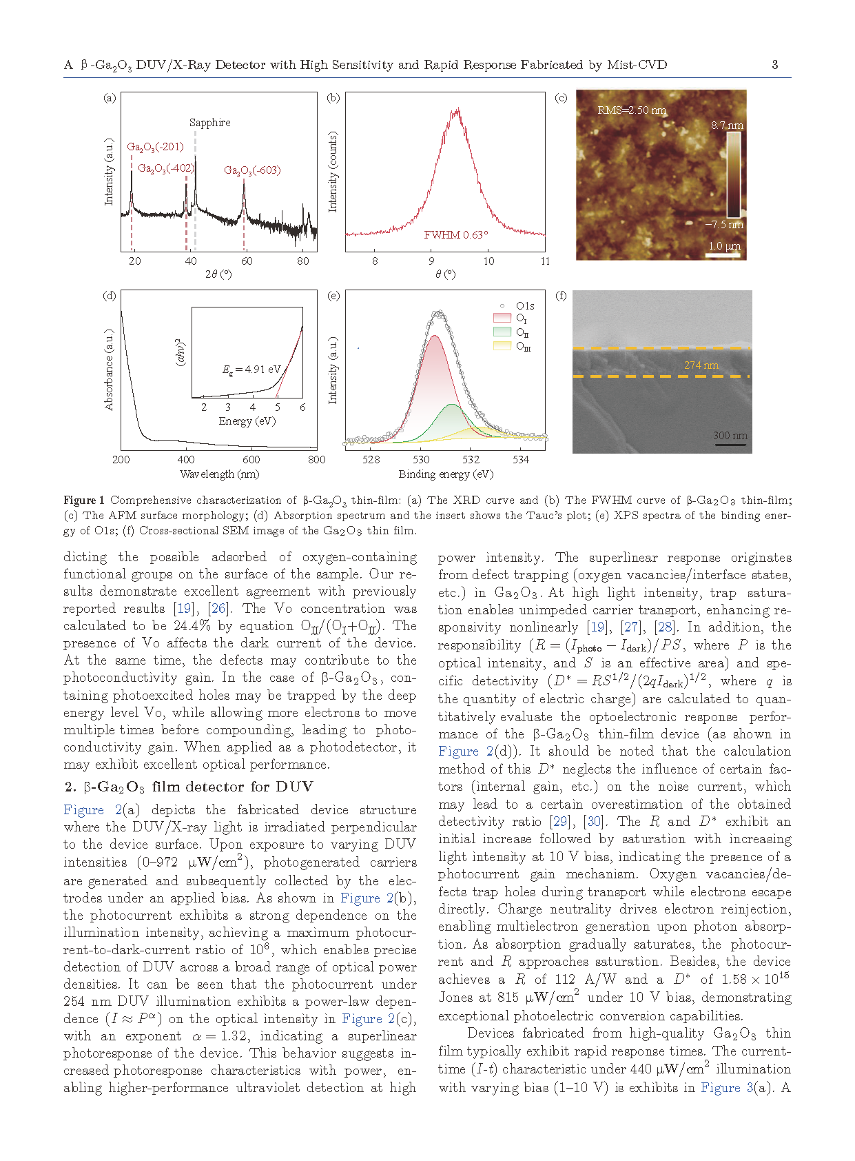
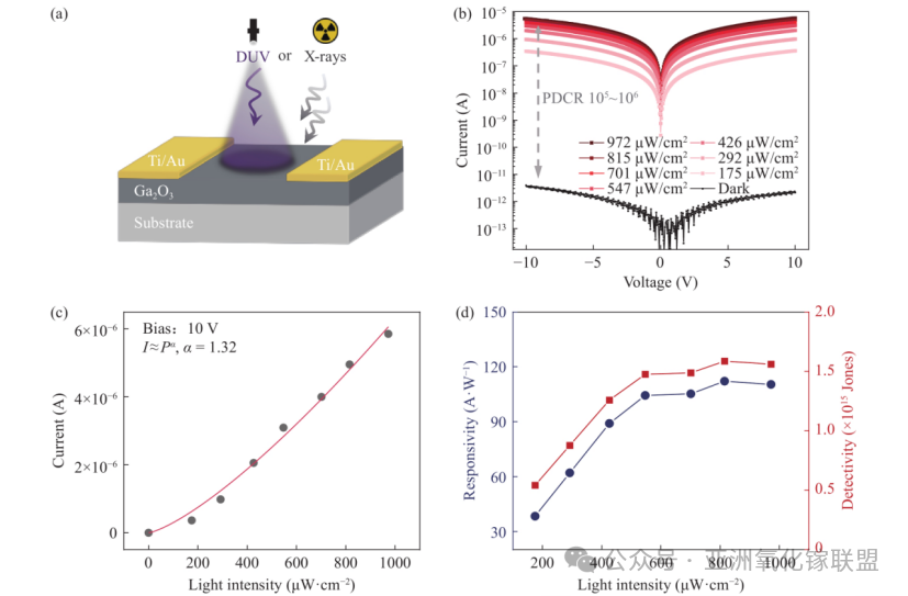
In DUV testing, the team observed a superlinear dependence of photocurrent on incident الضوء intensity—indicating that a small number of photons can trigger massive carrier transport across the device. This large photoconductive gain originates from moderate concentrations of deep-level defects (oxygen vacancies), which effectively trap holes.
More importantly, the Mist-CVD process enables precise control of defect density, maintaining oxygen vacancies within an optimal “sweet spot.” This balance ensures sufficient gain while preventing excessive carrier trapping.
As a result, the device achieves both high responsivity under solar-blind UV illumination and an ultrafast recovery time as short as 16 ms, overcoming the long-standing slow-response limitation of Ga₂O₃ detectors and enabling potential applications in real-time high-speed imaging.
Exceptional X-ray Sensitivity from Micron-Scale Films
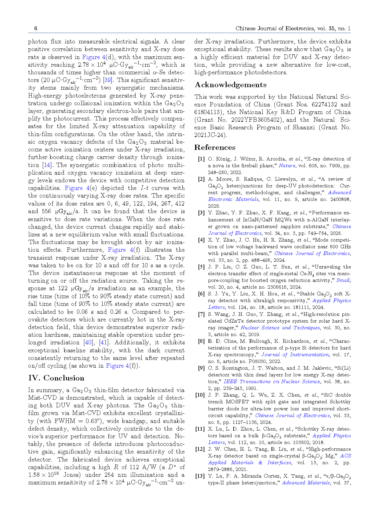
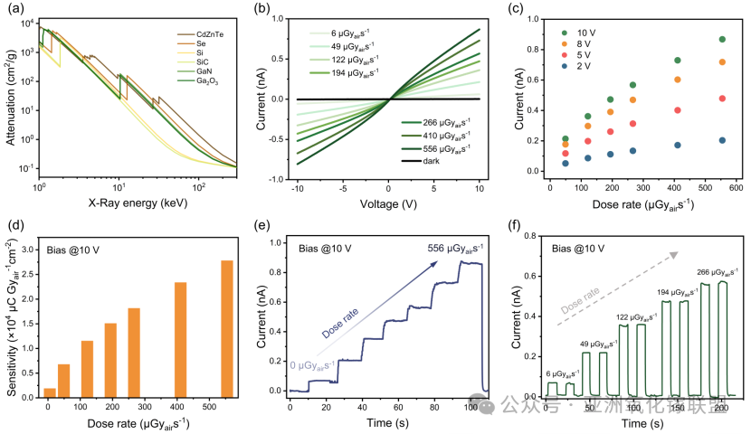
For applications such as medical imaging and nuclear inspection, efficient detection of high-energy radiation is critical. Owing to its high density and ultra-wide bandgap, Ga₂O₃ exhibits intrinsic advantages for X-ray detection.
Remarkably, despite using only micron-scale thin films, the fabricated detector produces highly consistent and sensitive linear photocurrent responses under extremely low X-ray doses.
Mechanistically, high-energy X-ray photons induce strong secondary electron avalanche ionization within the lattice. Combined with the activation of deep-level defects under radiation, these effects synergistically enhance device sensitivity, achieving values orders of magnitude higher than those of commercial amorphous selenium detectors used in medical imaging.
Moreover, under prolonged high-dose irradiation and repeated switching cycles, the device maintains an exceptionally stable dark current baseline without degradation or drift, demonstrating outstanding radiation hardness and long-term stability.
Application Prospects
The Mist-CVD process proposed in this work not only verifies the synergistic amplification effects of defect engineering on semiconductor optoelectronic behavior at the fundamental level, but also provides a practical route toward scalable fabrication of high-gain, fast-response dual-mode detectors.
Compared with traditional vacuum-based epitaxy, this approach offers a potentially disruptive cost advantage. In the future, this low-cost and high-stability DUV/X-ray detection technology is expected to enable large-scale solar-blind imaging systems, portable low-dose medical CT devices, and aerospace detection under extreme environments, contributing to the development of next-generation high-performance optoelectronic components.
Conclusion
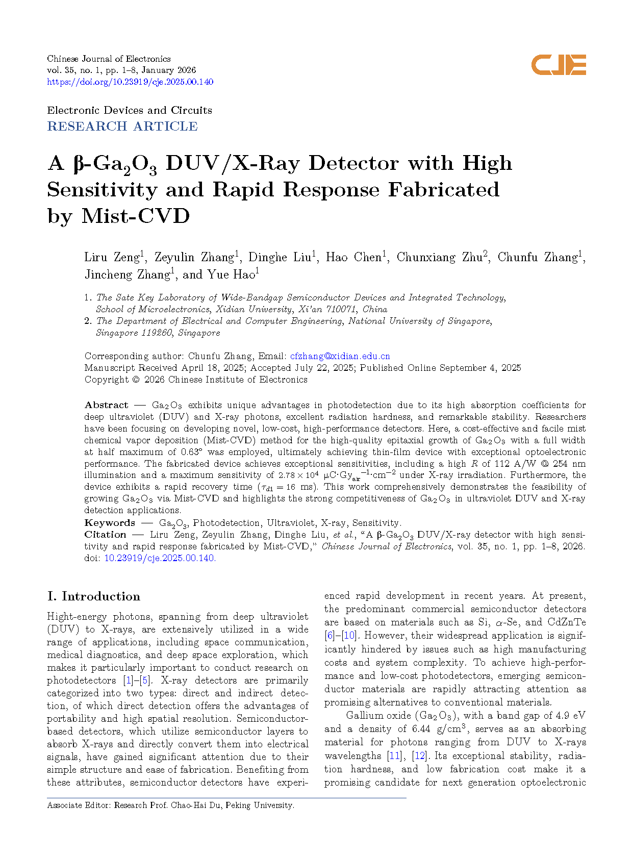
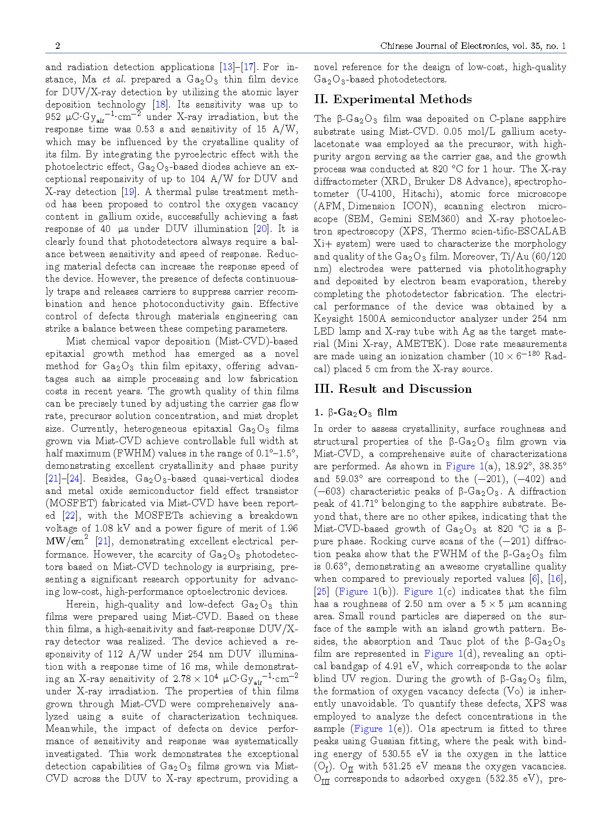
In summary, a Ga₂O₃ thin-film detector fabricated via Mist-CVD is demonstrated, which is capable of detecting both DUV and X-ray photons. The Ga₂O₃ thin film grown via Mist-CVD exhibits excellent crystallinity (FWHM = 0.63°), a wide bandgap, and a suitable defect density, which collectively contribute to the device’s superior performance in UV and X-ray detection.
Notably, the presence of defects introduces photoconductive gain, significantly enhancing the sensitivity of the detector. The fabricated device achieves outstanding performance, including a high responsivity (R) of 112 A/W and a specific detectivity (D*) of 1.58 × 10¹⁵ Jones under 254 nm illumination, as well as a maximum sensitivity of 2.78 × 10⁴ μC·Gyair⁻¹·cm⁻² under X-ray irradiation.
Furthermore, the device exhibits excellent stability. These results demonstrate that Ga₂O₃ is a highly efficient material for DUV and X-ray detection, providing a promising pathway toward low-cost, high-performance photodetectors.
DOI:
10.23919/cje.2025.00.140