Paper Sharing
【International Papers】Epitaxial β-Ga₂O₃/GaN Heterojunction Based UV C/UV A Photodetectors with Superior Responsivity and Stability Under Vertical and Lateral Mode Operations
日期:2026-04-24阅读:221
Researchers from the CSIR-National Physical Laboratory, Academy of Scientific and Innovative Research, Birla Institute of Technology and Science, Tamkang University, University of Petroleum and Energy Studies have published a dissertation titled ”Epitaxial β‑Ga₂O₃/GaN Heterojunction Based UV‑C/UV‑A Photodetectors with Superior Responsivity and Stability Under Vertical and Lateral Mode Operations” in Small.
Background
Conventional semiconductors (Si, GaAs) have relatively narrow bandgaps, requiring optical filters for deep UV detection, leading to system complexity. Among ultra-wide-bandgap semiconductors, β‑Ga₂O₃ (~4.9 eV) is suitable for solar-blind UV detection but suffers from low carrier mobility and defect-induced recombination. GaN exhibits high electron mobility and excellent near-UV responsivity. The n‑n type‑I β‑Ga₂O₃/GaN heterojunction enables dual-band UV detection, suppresses dark current, and improves responsivity and speed, showing great value in flame detection, space monitoring, environmental safety, and secure communications.
Abstract
We report the development of a high-performance, bias-tunable dual-band ultraviolet photodetector based on a type‑I β‑Ga₂O₃/GaN heterojunction fabricated by pulsed laser deposition (PLD). The device enables detection of 255 nm and 347 nm through bias control, exhibiting high responsivity and stable performance. Reflection high-energy electron diffraction, synchrotron X-ray diffraction, and X-ray photoelectron spectroscopy confirm the formation of a high-quality epitaxial β‑Ga₂O₃/GaN interface with favorable conduction‑ and valence-band offsets that enhance carrier generation and suppress recombination. The UV detection performance was evaluated in both vertical photodetector (VPD) and lateral photodetector (LPD) configurations. The VPD demonstrates responsivities of 19.8 A/W at 255 nm and 923.6 A/W at 347 nm under a low bias of 5 V, while the LPD achieves 365.7 A/W at 255 nm and 455.1 A/W at 347 nm under 40 V. The enhanced near-UV response arises from a synergistic mechanism combining photoconductive gain in β‑Ga₂O₃ and band-edge absorption in GaN, enabled by engineered band alignment. This work establishes a generalizable design strategy for next-generation dual-band UV photodetectors for flame detection, space-based monitoring, environmental safety, and secure communications.
Highlights
High-quality epitaxial type‑I β‑Ga₂O₃/GaN n‑n heterojunction fabricated by PLD with low interface defects and favorable band offsets;
Realizes bias-tunable dual-band UV detection covering UV‑C (255 nm) and UV‑A (347 nm);
Ultra-high responsivity: 923.6 A/W at 347 nm (VPD, 5 V) and 365.7 A/W at 255 nm (LPD, 40 V);
Low dark current, fast switching speed, and excellent stability over 100 ON/OFF cycles;
Reveals carrier separation and transport mechanism in type‑I heterojunction, with high electron mobility of GaN greatly boosting photoconductive gain.
Conclusion
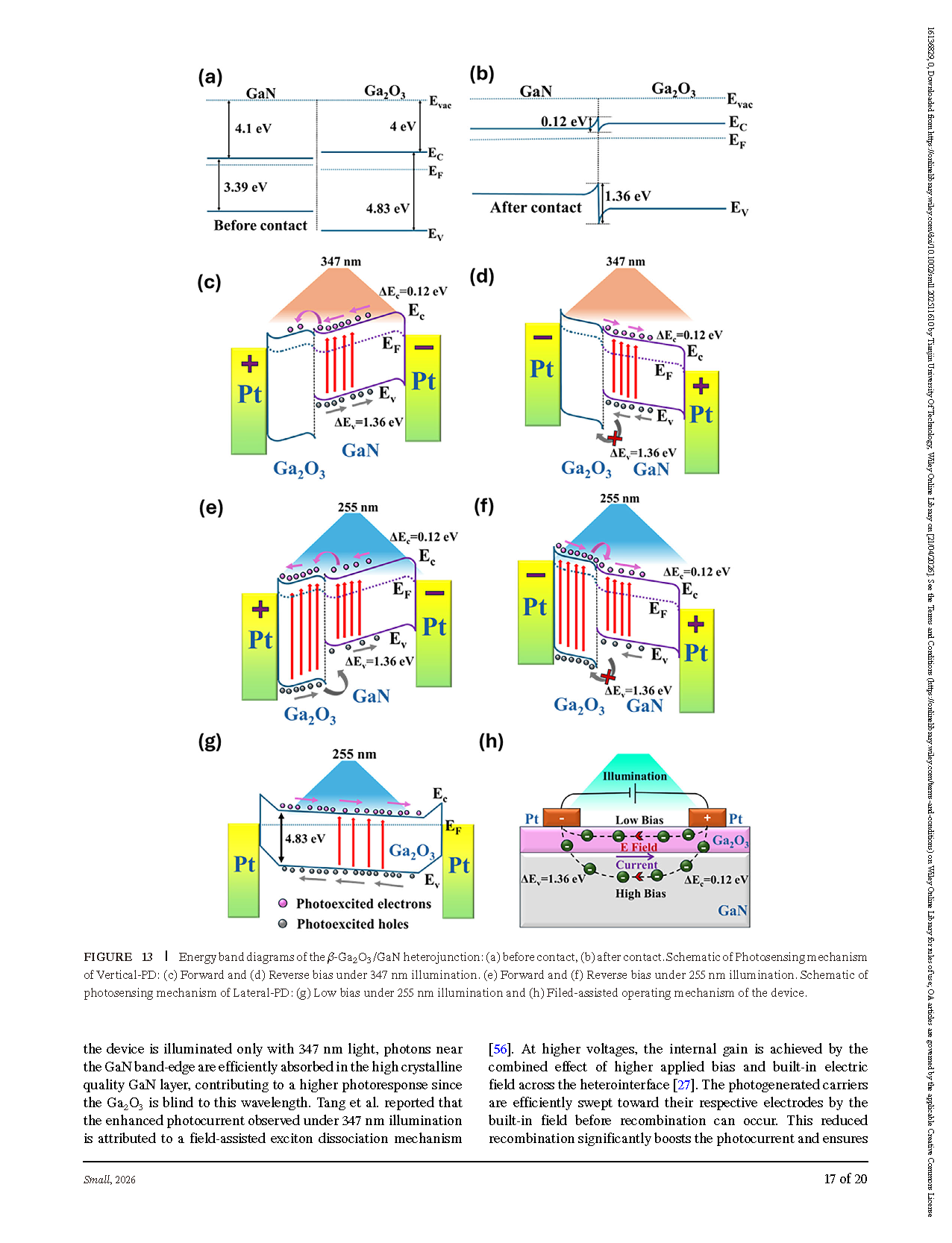
We have developed and systematically characterized a high-performance dual-band ultraviolet photodetector based on a type‑I β‑Ga₂O₃/GaN heterojunction, grown via pulsed laser deposition. The device architecture leverages the ultra-wide bandgap and high breakdown strength of β‑Ga₂O₃, integrated with the superior electron mobility of GaN, to achieve a synergistically enhanced optoelectronic response. Through comprehensive structural and interfacial analyses, we confirm the formation of a high-quality, epitaxial oxide–nitride interface with a favourable type‑I band alignment that facilitates efficient carrier generation, separation, and collection. The fabricated β‑Ga₂O₃/GaN heterostructure photodetector demonstrates excellent performance across both the UV‑C (255 nm) and UV‑A (347 nm) regimes. Under a moderate bias of 5 V, the responsivity reaches 19.8 A/W at 255 nm and a remarkably high value of 923.6 A/W at 347 nm, indicating a significantly enhanced photoresponse near the GaN band edge. These results confirm that while the deep-UV response is dominated by photoconductive generation in β‑Ga₂O₃, the near-UV response benefits from the band-edge absorption in the GaN layer, yielding substantially higher gain due to strong internal photoconductive amplification and suppressed dark current enabled by the engineered band offsets and interfacial charge dynamics. Moreover, the device maintains robust operational stability under prolonged UV exposure, further validating its viability for real-world deployment. Overall, the device exhibits strong dual-band UV detectivity, bias-tunable photoresponse, and high responsivity, making it a promising candidate for both solar-blind and near-UV photodetection applications. This work not only establishes the β‑Ga₂O₃/GaN platform as a competitive and scalable solution for next-generation ultraviolet photodetection but also provides a generalizable design strategy for band-aligned heterostructures that transcend the limitations of conventional wide-bandgap semiconductors. The demonstrated performance and stability position this architecture as a strong candidate for critical applications in flame sensing, space-based UV monitoring, biological sterilization, and other environments requiring fast, sensitive, and reliable UV detection.
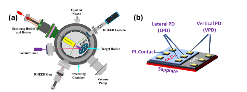
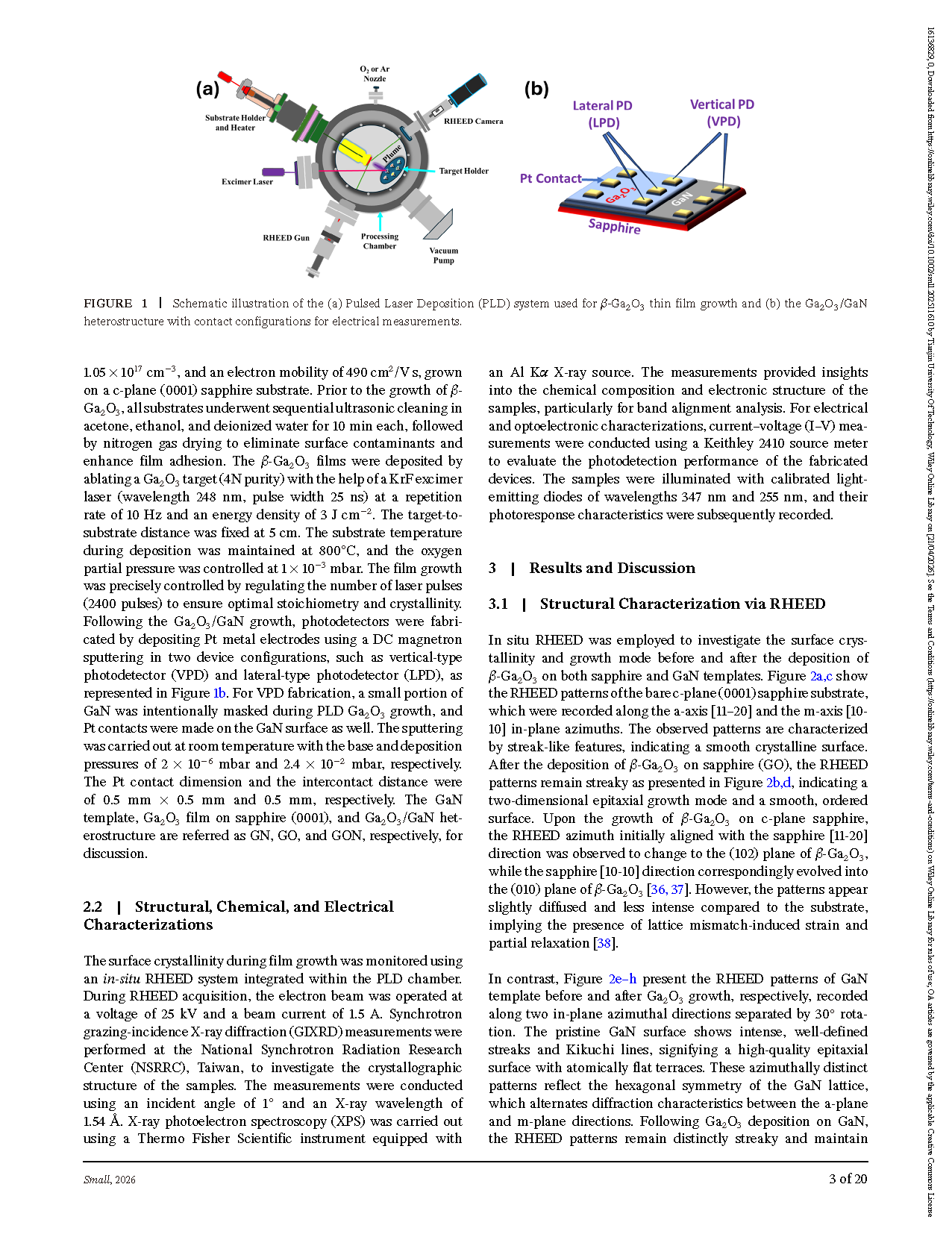
Figure 1 Schematic illustration of the (a) Pulsed Laser Deposition (PLD) system used for β-Ga₂O₃ thin film growth and (b) the Ga₂O₃/GaN heterostructure with contact configurations for electrical measurements.
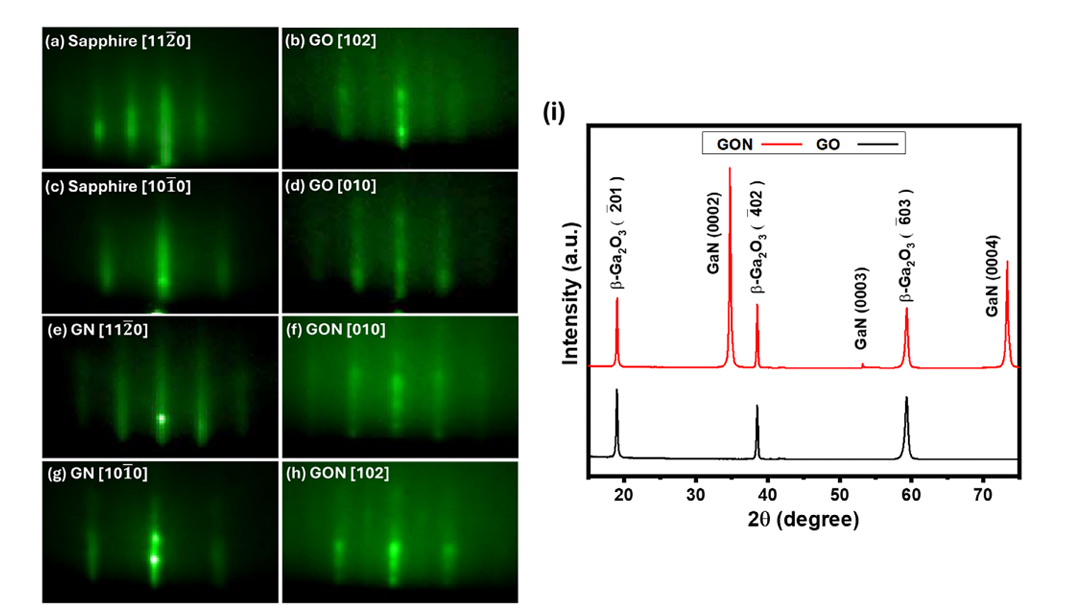
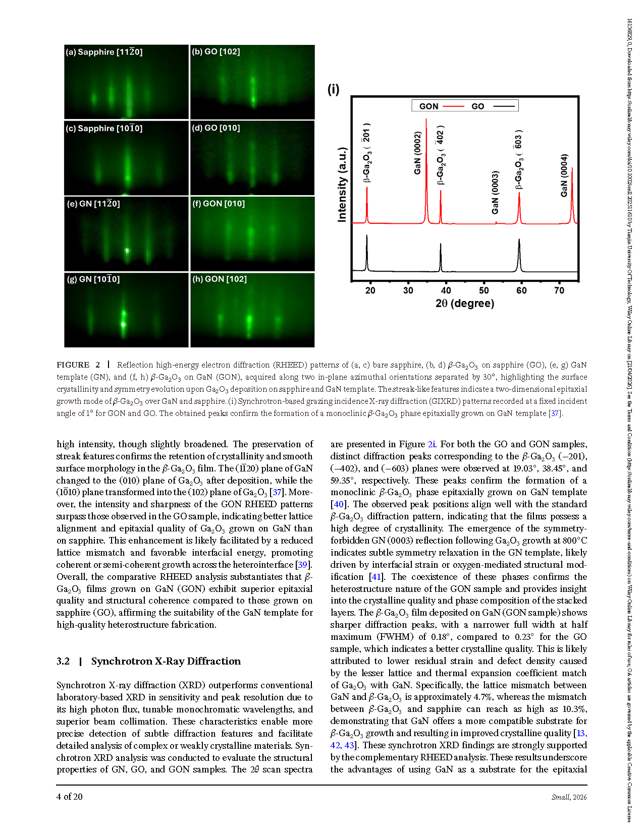
Figure 2 Reflection high-energy electron diffraction (RHEED) patterns of (a, c) bare sapphire, (b, d) β-Ga₂O₃ on sapphire (GO), (e, g) GaN template (GN), and (f, h) β-Ga₂O₃ on GaN (GON), acquired along two in-plane azimuthal orientations separated by 30°, highlighting the surface crystallinity and symmetry evolution upon Ga₂O₃ deposition on sapphire and GaN template. The streak-like features indicate a two-dimensional epitaxial growth mode of β-Ga₂O₃ over GaN and sapphire. (i) Synchrotron-based grazing incidence X-ray diffraction (GIXRD) patterns recorded at a fixed incident angle of 1° for GON and GO. The obtained peaks confirm the formation of a monoclinic β-Ga₂O₃ phase epitaxially grown on GaN template.
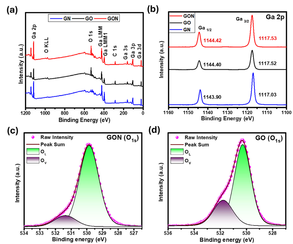
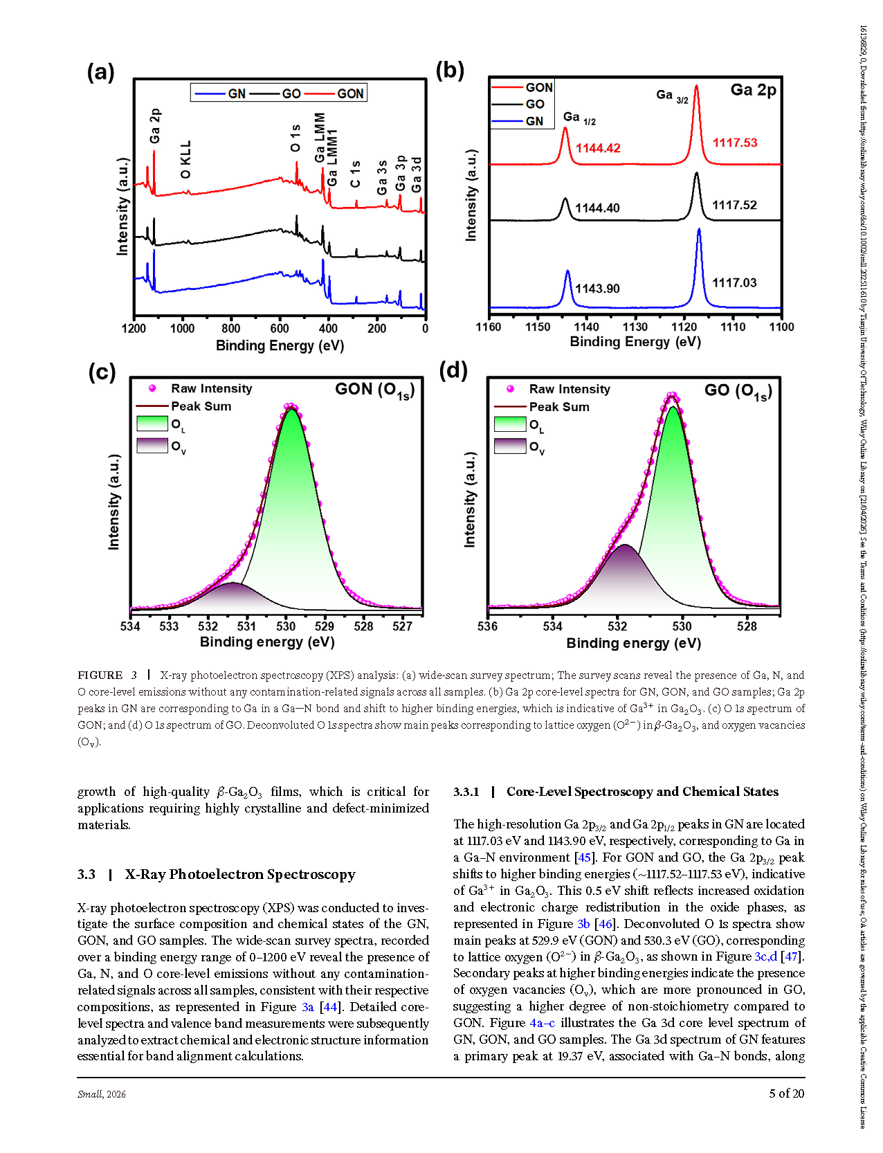
Figure 3 X-ray photoelectron spectroscopy (XPS) analysis: (a) wide-scan survey spectrum; The survey scans reveal the presence of Ga, N, and O core-level emissions without any contamination-related signals across all samples. (b) Ga 2p core-level spectra for GN, GON, and GO samples; Ga 2p peaks in GN are corresponding to Ga in a Ga─N bond and shift to higher binding energies, which is indicative of Ga³⁺ in Ga₂O₃. (c) O 1s spectrum of GON; and (d) O 1s spectrum of GO. Deconvoluted O 1s spectra show main peaks corresponding to lattice oxygen (O²⁻) in β-Ga₂O₃, and oxygen vacancies (Oᵥ).
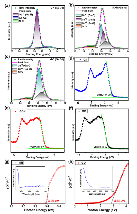
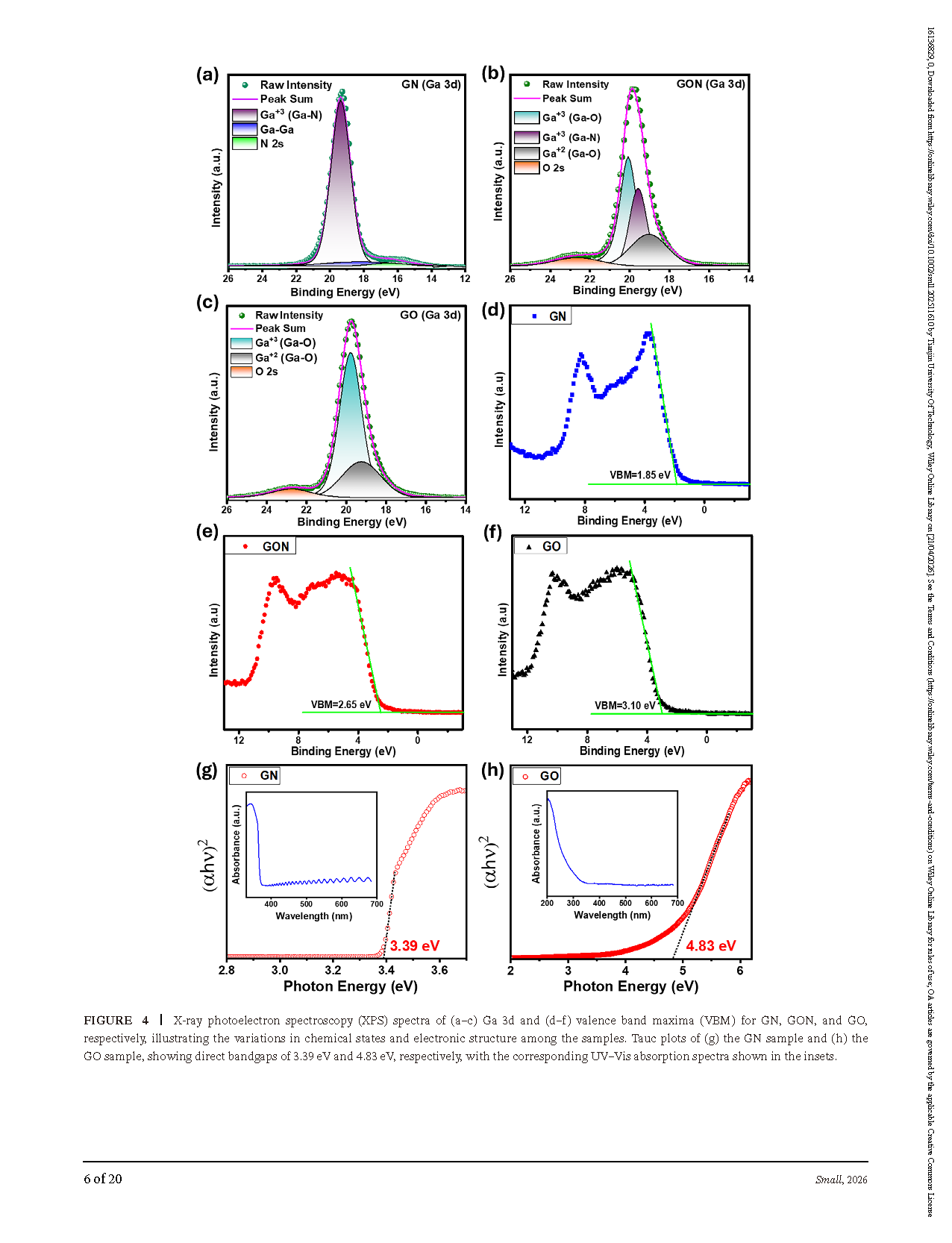
Figure 4 X-ray photoelectron spectroscopy (XPS) spectra of (a–c) Ga 3d and (d–f) valence band maxima (VBM) for GN, GON, and GO, respectively, illustrating the variations in chemical states and electronic structure among the samples. Tauc plots of (g) the GN sample and (h) the GO sample, showing direct bandgaps of 3.39 eV and 4.83 eV, respectively, with the corresponding UV–Vis absorption spectra shown in the insets.
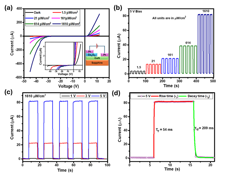
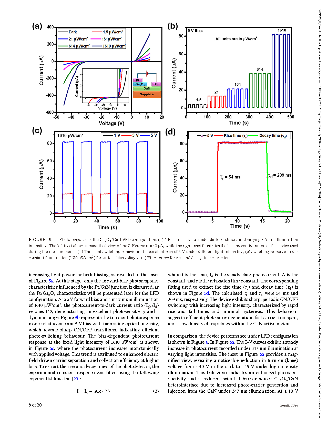
Figure 5 Photo-response of the Ga₂O₃/GaN VPD configuration: (a) I–V characteristics under dark conditions and varying 347 nm illumination intensities. The left inset shows a magnified view of the I–V curve near 0 µA, while the right inset illustrates the biasing configuration of the device used during the measurements. (b) Transient switching behaviour at a constant bias of 5 V under different light intensities, (c) switching response under constant illumination (1610 µW/cm²) for various bias voltages. (d) Fitted curve for rise and decay time.
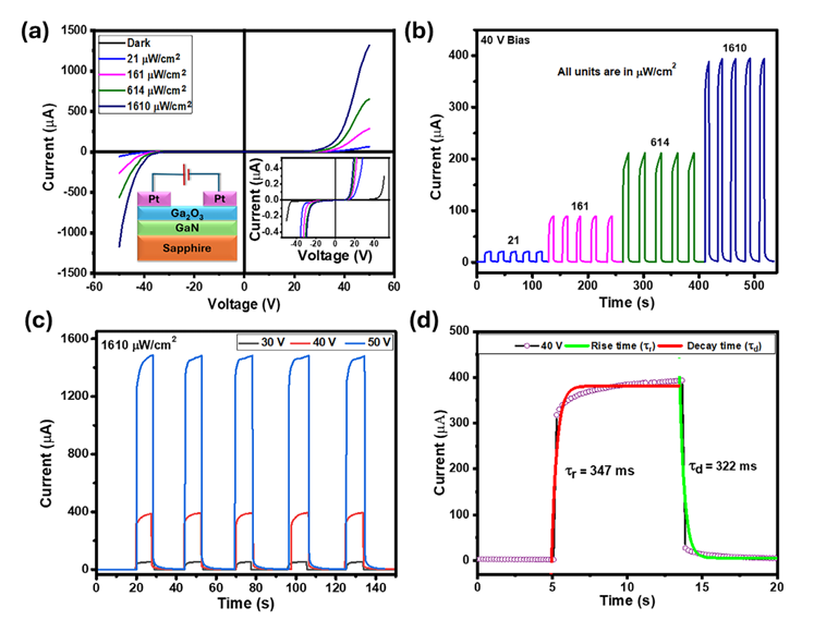
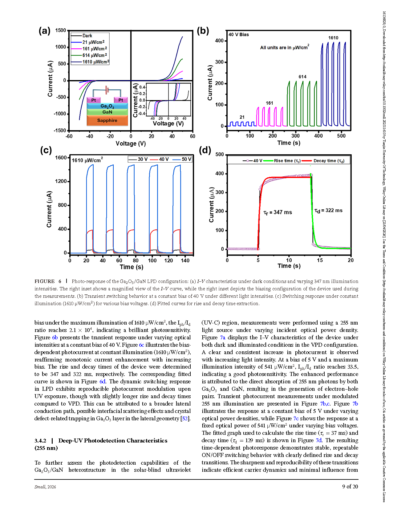
Figure 6 Photo-response of the Ga₂O₃/GaN LPD configuration: (a) I–V characteristics under dark conditions and varying 347 nm illumination intensities. The right inset shows a magnified view of the I–V curve, while the right inset depicts the biasing configuration of the device used during the measurements. (b) Transient switching behavior at a constant bias of 40 V under different light intensities. (c) Switching response under constant illumination (1610 µW/cm²) for various bias voltages. (d) Fitted curves for rise and decay time
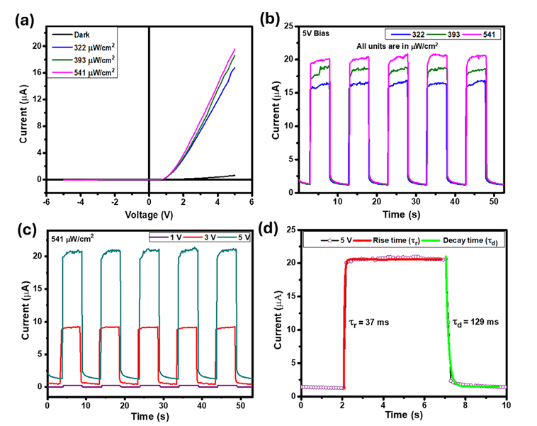
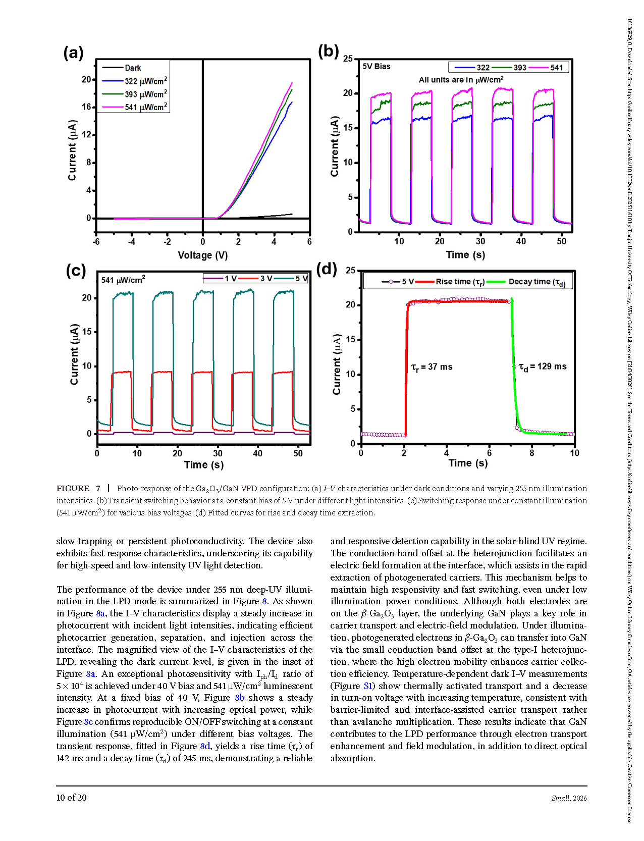
Figure 7 Photo-response of the Ga₂O₃/GaN VPD configuration: (a) I–V characteristics under dark conditions and varying 255 nm illumination intensities. (b) Transient switching behavior at a constant bias of 5 V under different light intensities. (c) Switching response under constant illumination (541 µW/cm²) for various bias voltages. (d) Fitted curves for rise and decay time extraction.
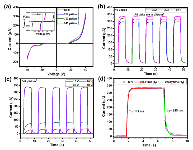
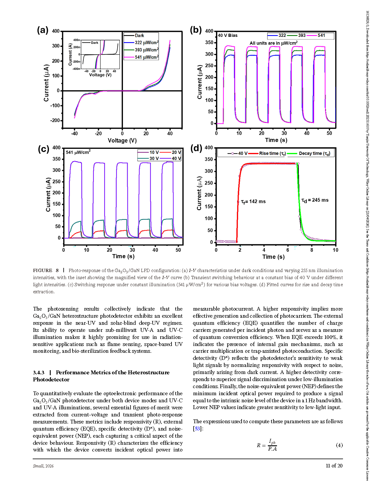
Figure 8 Photo-response of the Ga₂O₃/GaN LPD configuration: (a) I–V characteristics under dark conditions and varying 255 nm illumination intensities, with the inset showing the magnified view of the I–V curve (b) Transient switching behaviour at a constant bias of 40 V under different light intensities. (c) Switching response under constant illumination (541 µW/cm²) for various bias voltages. (d) Fitted curves for rise and decay time extraction.
DOI:
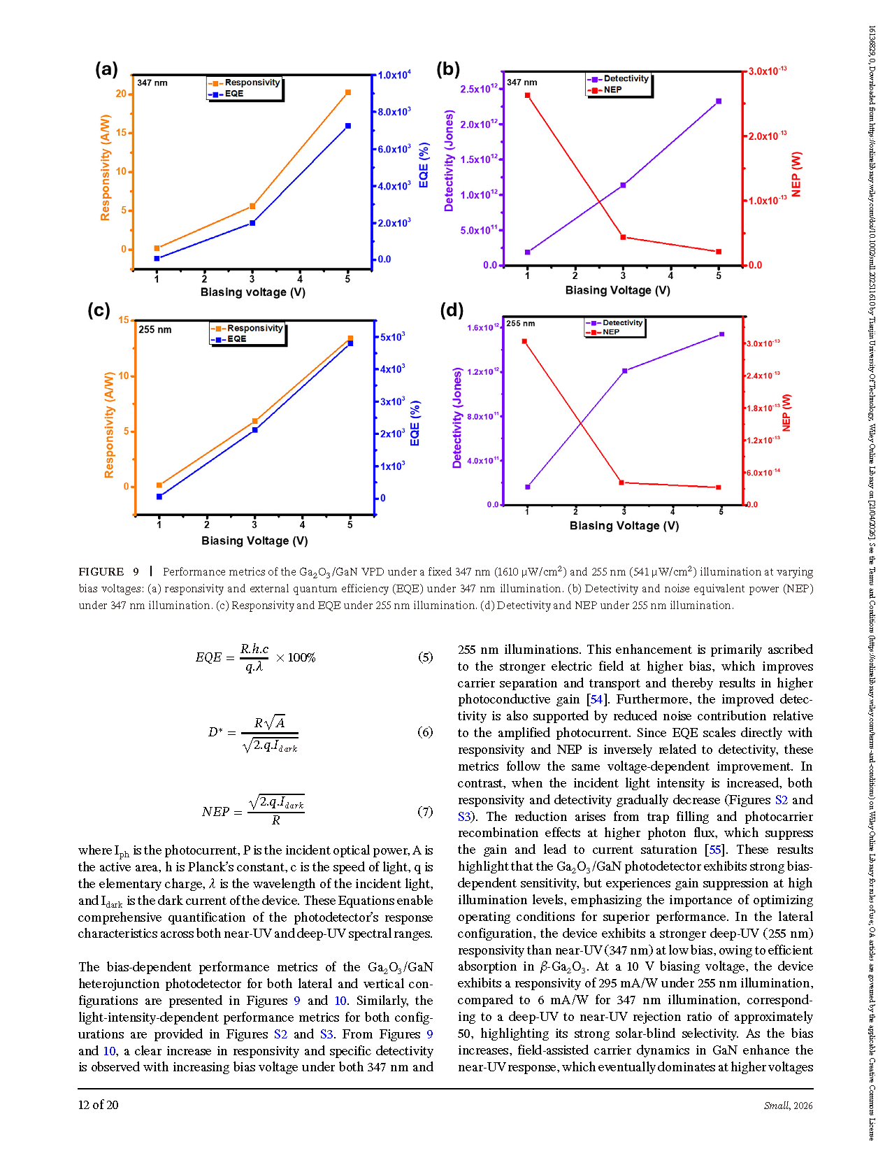
doi.org/10.1002/smll.202511610