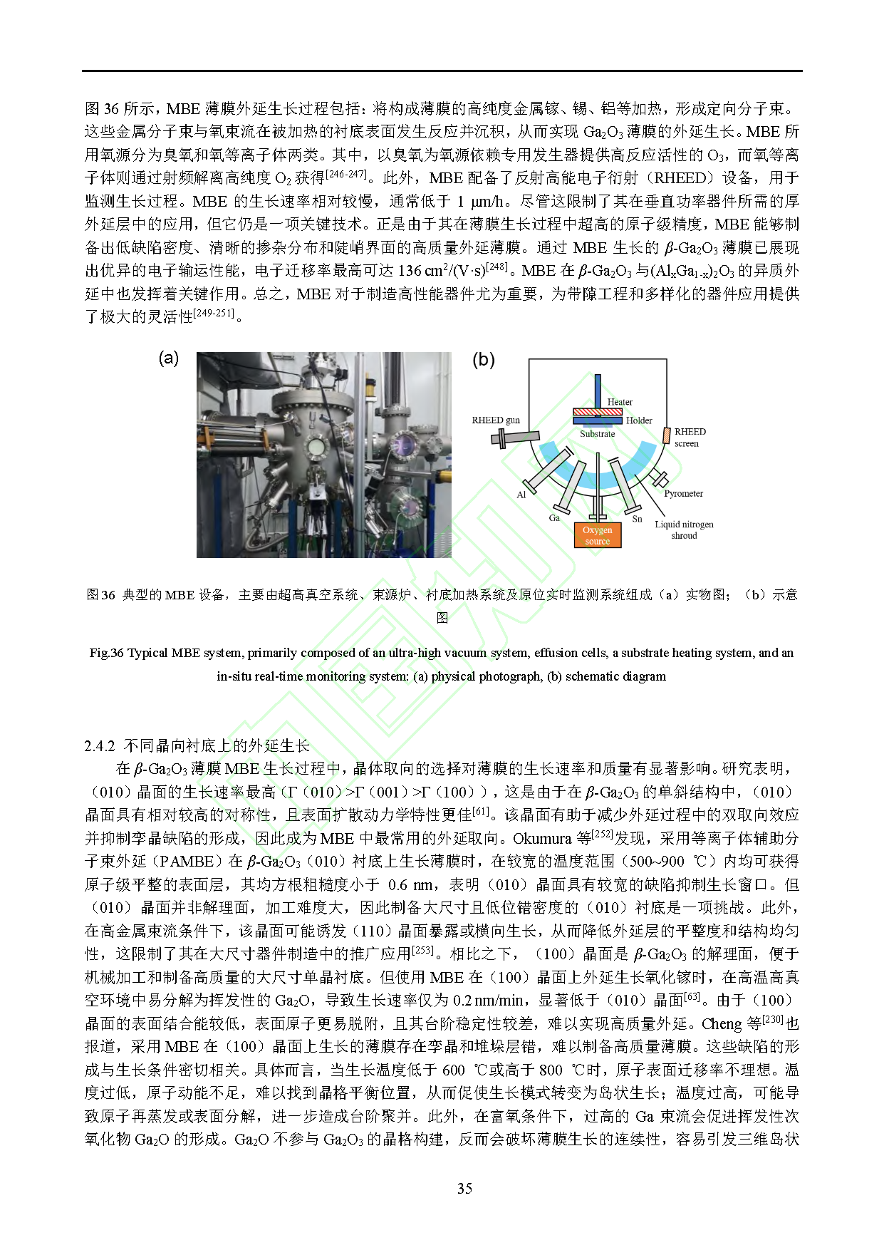
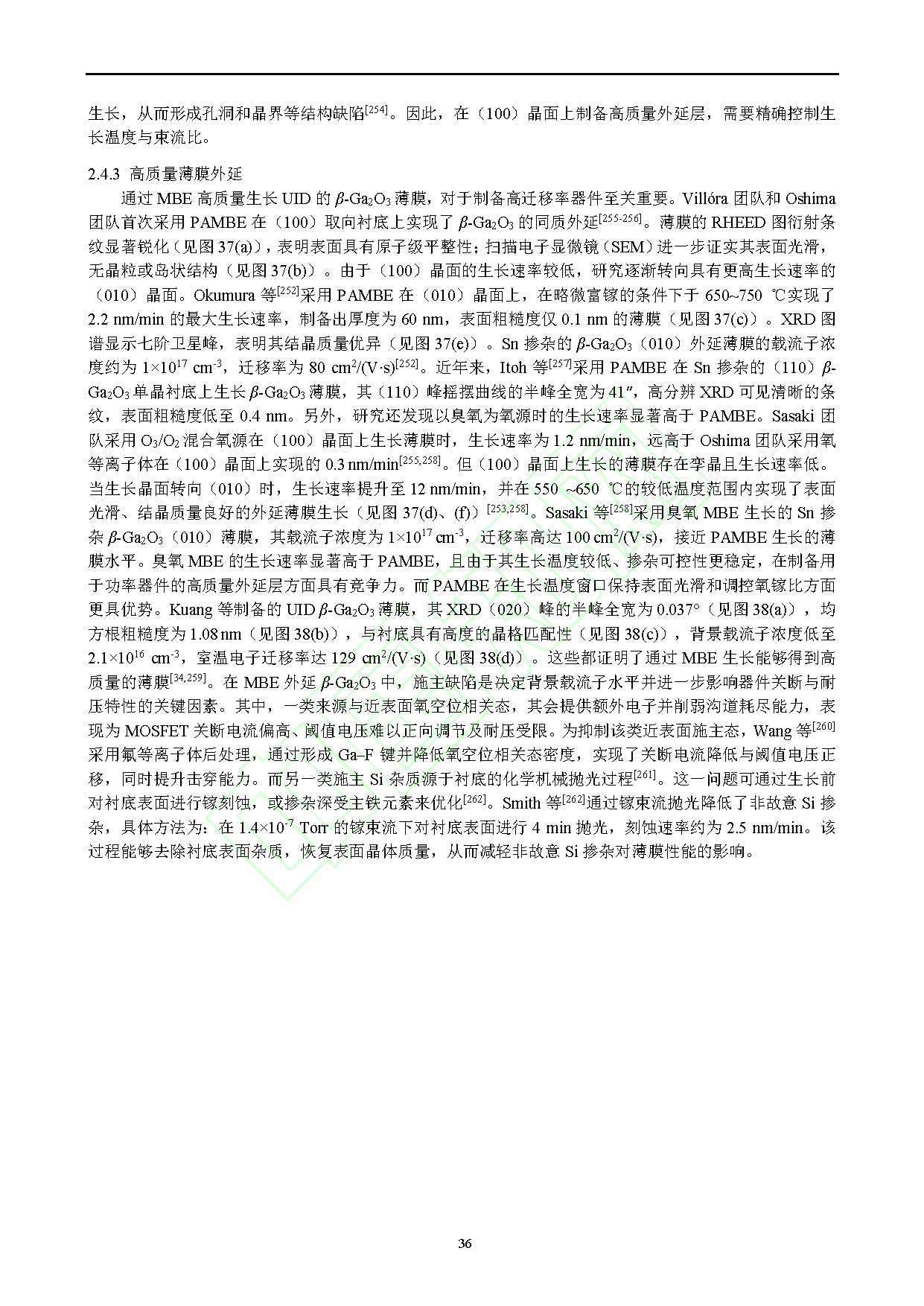
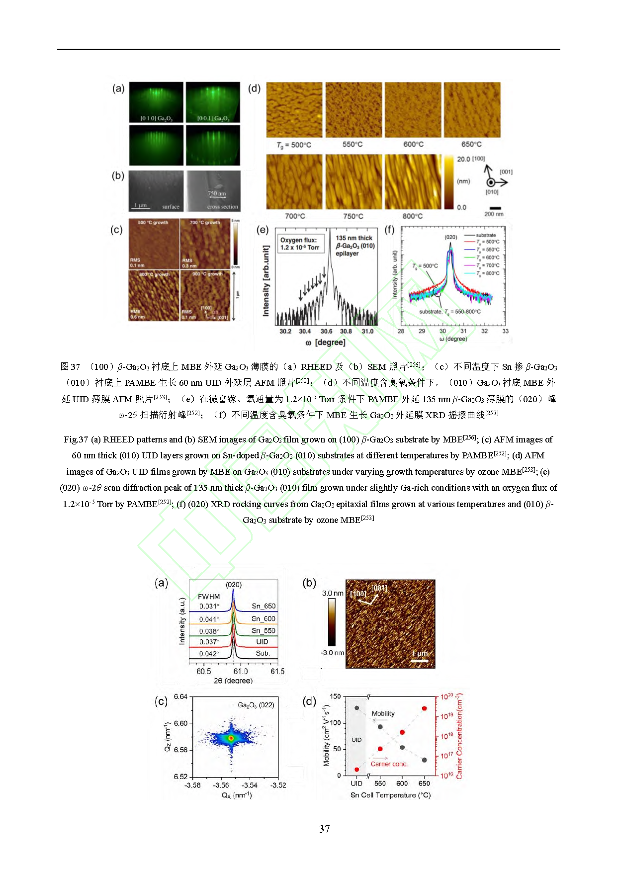
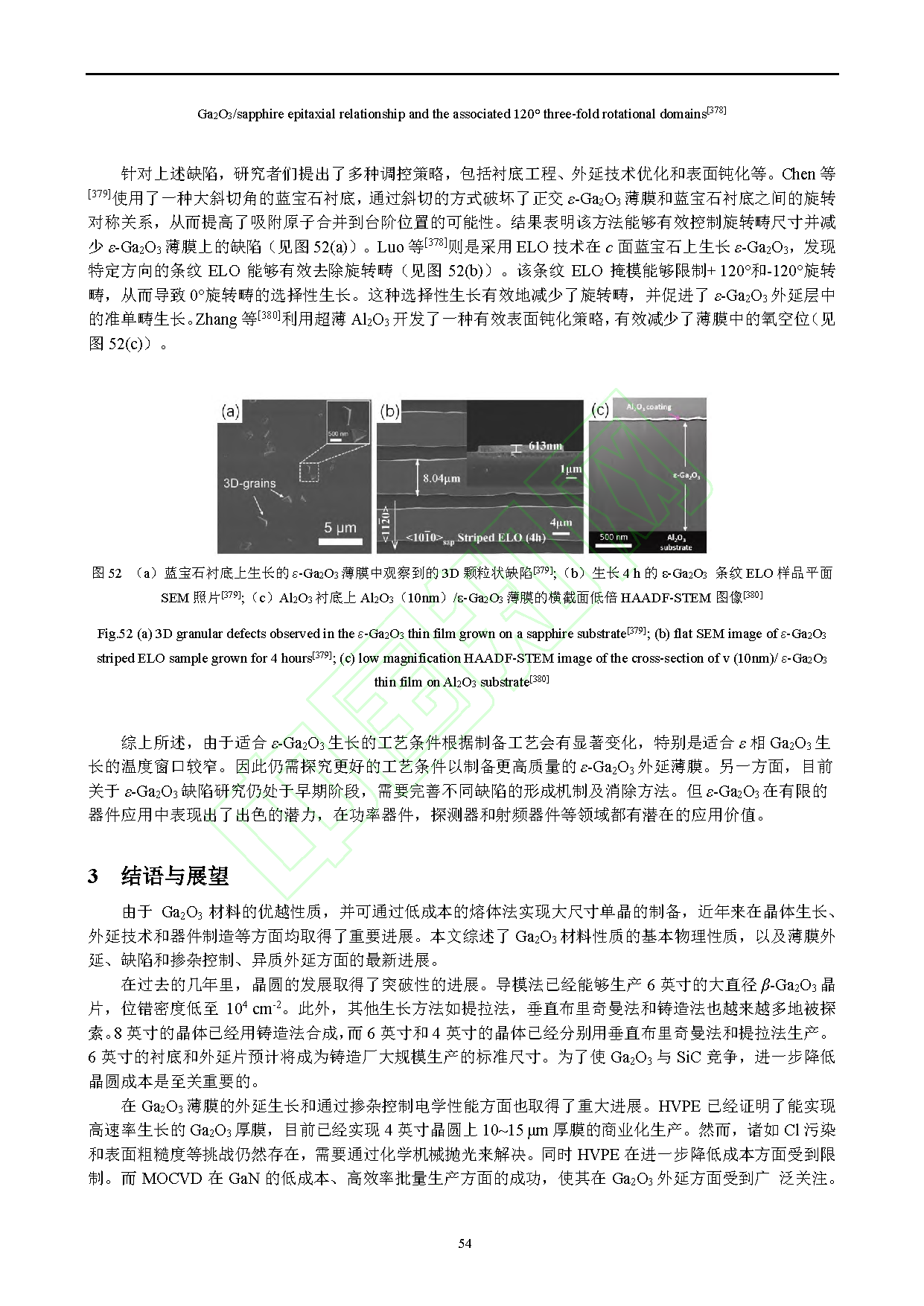
Paper Sharing
【Member Papers】Research Progress in the Epitaxy, Doping Control, and Defect Management of Gallium Oxide Thin Films
日期:2026-04-24阅读:291
A joint research team involving Prof. Hongliang Zhang from Xiamen University, Researcher Hongji Qi from the Shanghai Institute of Optics and Fine Mechanics and Shanghai Key Laboratory of Wide and Ultra-Wide Bandgap Semiconductor Materials, has published a review article entitled “Research Progress in the Epitaxy, Doping Control, and Defect Management of Gallium Oxide Thin Films” in the Journal of Synthetic Crystals.
Background
Gallium oxide (Ga2O3) is an ultra-wide-bandgap semiconductor of great strategic importance. It possesses a bandgap of approximately 4.9 eV and a theoretical critical breakdown field as high as 8 MV/cm. Its Baliga’s figure of merit is markedly superior to that of SiC and GaN, giving it enormous application potential in high-power electronic devices, radio-frequency front-end devices, and solar-blind ultraviolet photodetection. More importantly, Ga2O3 can be prepared as large-size, low-cost, high-quality single-crystal substrates via melt-growth methods. This unique advantage makes it more competitive for commercialization than other ultra-wide-bandgap materials such as AlN and diamond. Epitaxial thin films serve as the key bridge between single-crystal substrates and high-performance devices. Their crystal quality, surface morphology, doping concentration, and defect distribution directly determine the ultimate device performance, including breakdown voltage and on-resistance. At present, however, Ga2O3 epitaxy still faces major challenges in the effective suppression of background carriers, precise control of n-type doping, rapid growth of large-area high-quality thick films, and the reduction of defects such as dislocations and twins. In addition, p-type doping in Ga2O3 remains a critical bottleneck for the development of bipolar devices because of its band-structure limitations and strong self-compensation effects.
Abstract
This review systematically surveys the current research status of β-Ga2O3 epitaxial thin films. It introduces the fundamental principles and technical characteristics of mainstream epitaxial techniques, including HVPE, MOCVD, and MBE. Furthermore, it critically reviews representative recent advances in several core issues, including background carrier suppression, precise n-type doping control, thick-film growth, and defect evolution mechanisms. Moreover, this review analyzes the underlying reasons for the long-standing limitations of p-type doping in Ga2O3 from the perspective of physical mechanisms. It systematically summarizes the frontier explorations in the heteroepitaxy of different Ga2O3 polymorphs. Combined with existing technological bottlenecks, it provides a outlook on the future development directions of large-size growth, thick film epitaxy, and defect control of Ga2O3, offering vital references and guidance for driving technological breakthroughs and the commercialization process of Ga2O3 epitaxial materials.
Highlights
Systematic comparison of mainstream epitaxial techniques: Based on the fundamental principles and technical characteristics of HVPE, MOCVD, and MBE, the review provides a systematic comparison in terms of growth rate, doping controllability, and respective advantages and limitations, thereby offering a clear basis for selecting suitable technological routes for different application scenarios.
Electrical property modulation:The review summarizes the latest strategies for suppressing background carrier concentration and achieving high-precision n-type doping over a wide concentration range, providing systematic technical guidance for the electrical-property engineering of high-performance epitaxial films.
Thick-film growth and large-area epitaxy: In conjunction with the current development status of different epitaxial techniques, the review discusses the key challenges and corresponding strategies for rapid β-Ga2O3 thick-film growth, surface-quality optimization, and large-area epitaxy, offering important technical references for scalable epitaxial fabrication.
Defect formation mechanisms and suppression strategies: From the perspectives of crystallographic-plane characteristics and nucleation behavior, the review summarizes the formation mechanisms and suppression approaches for defects such as twins, stacking faults, dislocations, and particulates.
Analysis of the challenges in p-type doping: The review provides an in-depth analysis of the fundamental obstacles to p-type doping from the viewpoints of electronic structure and defect compensation, and summarizes related exploratory efforts.
Frontier progress in heteroepitaxy: Aimed at the requirements of of large-area growth and high-performance power devices, the review summarizes and discusses the progress and future trends in the heteroepitaxy of different Ga2O3 polymorphs.
Summary
In recent years, with the continued maturation of melt-growth technologies for large-size single crystals, -Ga2O3 has achieved important breakthroughs in crystal growth, epitaxial technology, and device fabrication. The edge-defined film-fed growth method has enabled the stable production of 6-inch Ga2O3 wafers with dislocation densities as low as 104 cm-2. Meanwhile, other approaches, such as the Czochralski method, vertical Bridgman growth, and casting methods, have also made encouraging progress. 6-inch substrates and epitaxial wafers are expected to become the standard size for large-scale wafer foundry manufacturing. In terms of epitaxy, HVPE has already realized the commercial production of 10-15 -thick films on 4-inch wafers. Owing to its advantages in low-cost mass production, MOCVD has attracted widespread attention and has achieved high-quality Ga2O3 epitaxy on both (010) and (100) oriented substrates. Using Si dopants, carrier concentrations can be controlled from 1015 cm-3 to 1020 cm-3, with electron mobility reaching up to 200 cm2/(V·s). By contrast, MBE offers unique advantages in atomic-level precision and plays a vital role in the growth of thin films with low defect densities, precise doping profiles, and abrupt interfaces. These features make it particularly suitable for constructing (AlxGa1-x)2O3/Ga2O3 two-dimensional electron gas structures for radio-frequency devices.
Currently, the industrialization of β-Ga2O3 still faces two major bottlenecks. One major challenge lies in the lack of effective p-type doping, which limits the realization of homoepitaxial PN-junction device structures. The other stems from its intrinsically low thermal conductivity, which leads to pronounced self-heating under high-power-density operating conditions. To address these challenges, large-area high-quality epitaxy and precise defect control are essential foundations for scalable devices and cost reduction. Interface engineering and heterostructure design have become effective routes for regulating carrier transport and electric-field distribution in the absence of a breakthrough in p-type doping. In parallel, thermal-management strategies represented by the heterogeneous integration of high-thermal-conductivity substrates are crucial for improving device stability. This systematic review provides important theoretical support and directional guidance for the technological development and industrial advancement of Ga2O3 epitaxial materials.
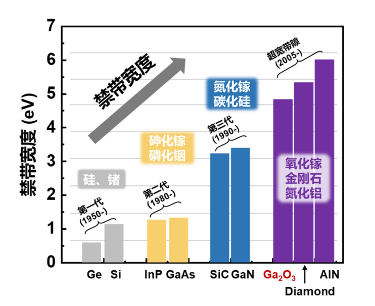
Fig.1 Schematic comparison of the bandgaps of various semiconductor materials. From left to right are the first-generation semiconductors (Si, Ge), second-generation semiconductors (GaAs, GaP), wide-bandgap materials (GaN, SiC), and ultra-widebandgap materials (β-Ga2O3, diamond, AlN)
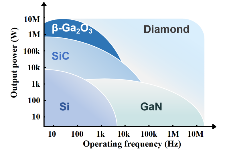
Fig.2 Application of Si, GaN, SiC, β-Ga2O3 and diamond under different requirements for output power and operating frequency
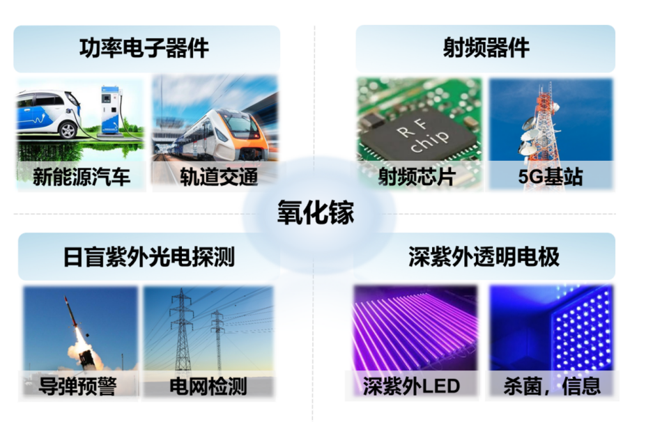
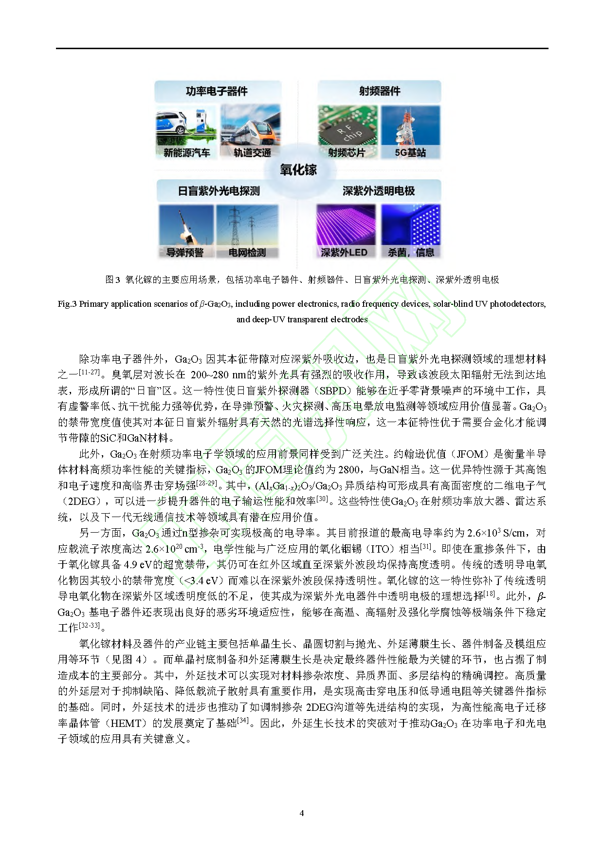
Fig.3 Primary application scenarios of β-Ga2O3, including power electronics, radio frequency devices, solar-blind UV photodetectors, and deep-UV transparent electrodes
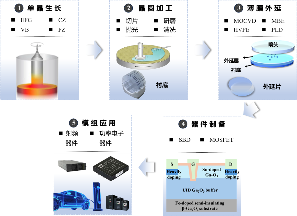
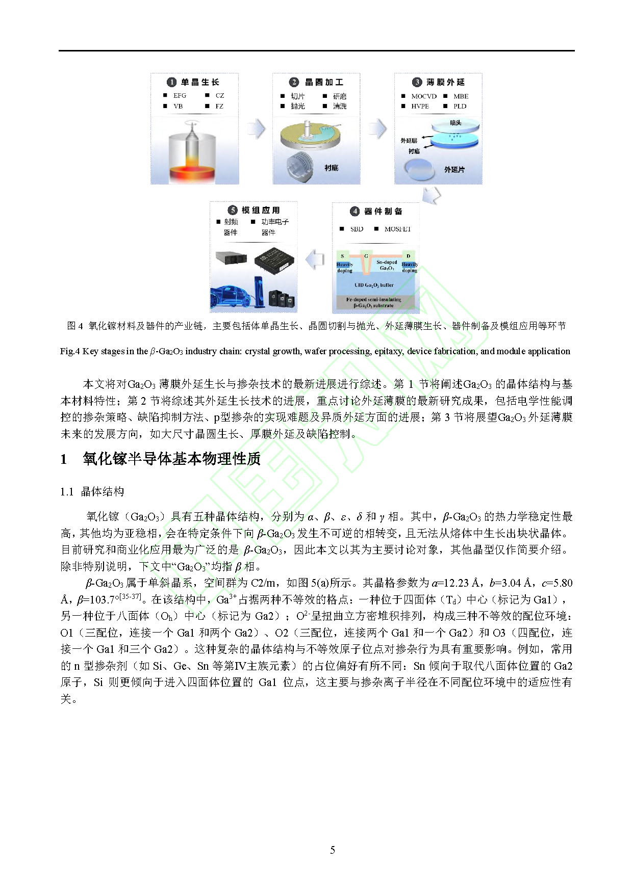
Fig.4 Key stages in the β-Ga2O3 industry chain: crystal growth, wafer processing, epitaxy, device fabrication, and module application
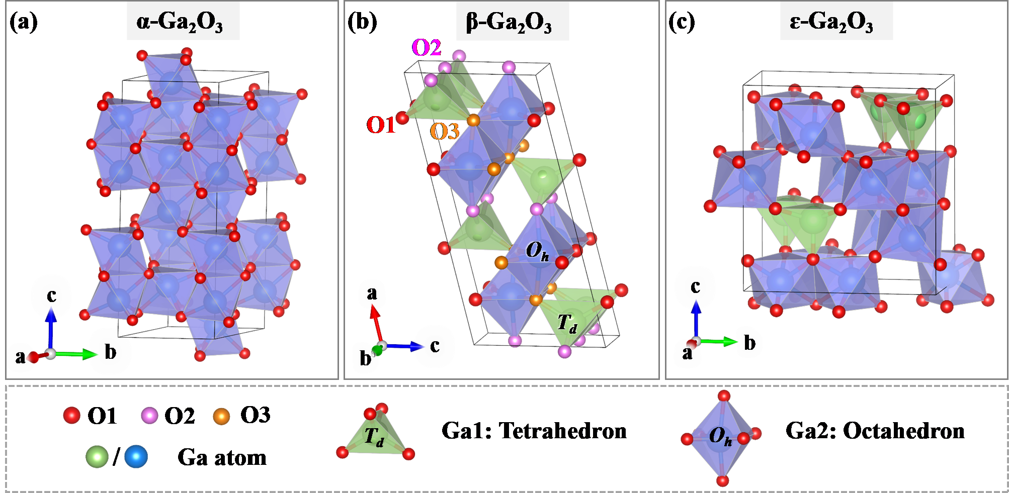
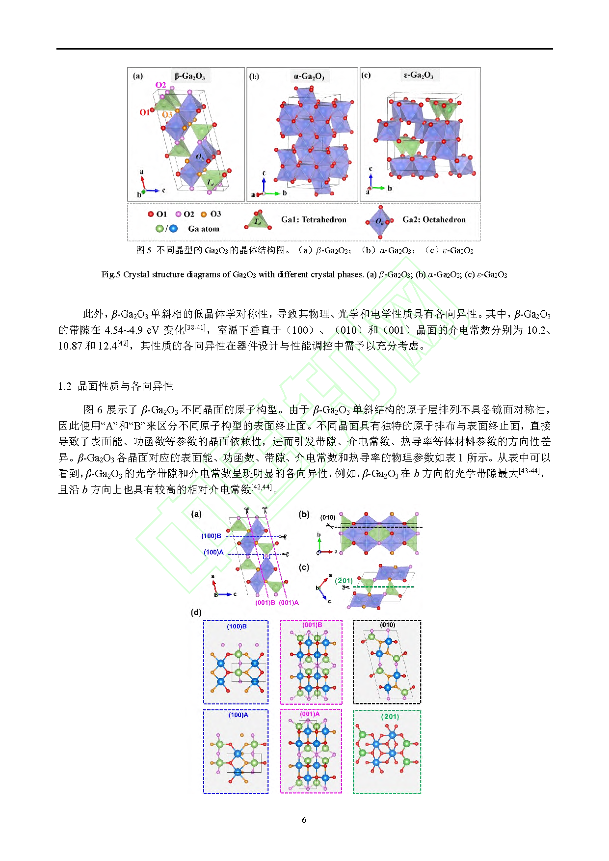
Fig.5 Crystal structure diagrams of Ga₂O₃ with different crystal phases. (a) β-Ga2O3; (b) Ga2O3; (c) ε-Ga2O3
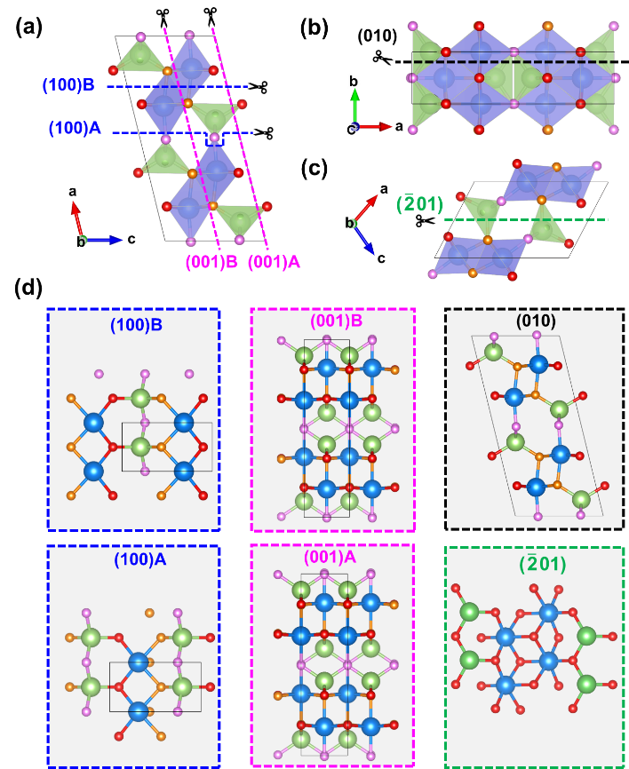
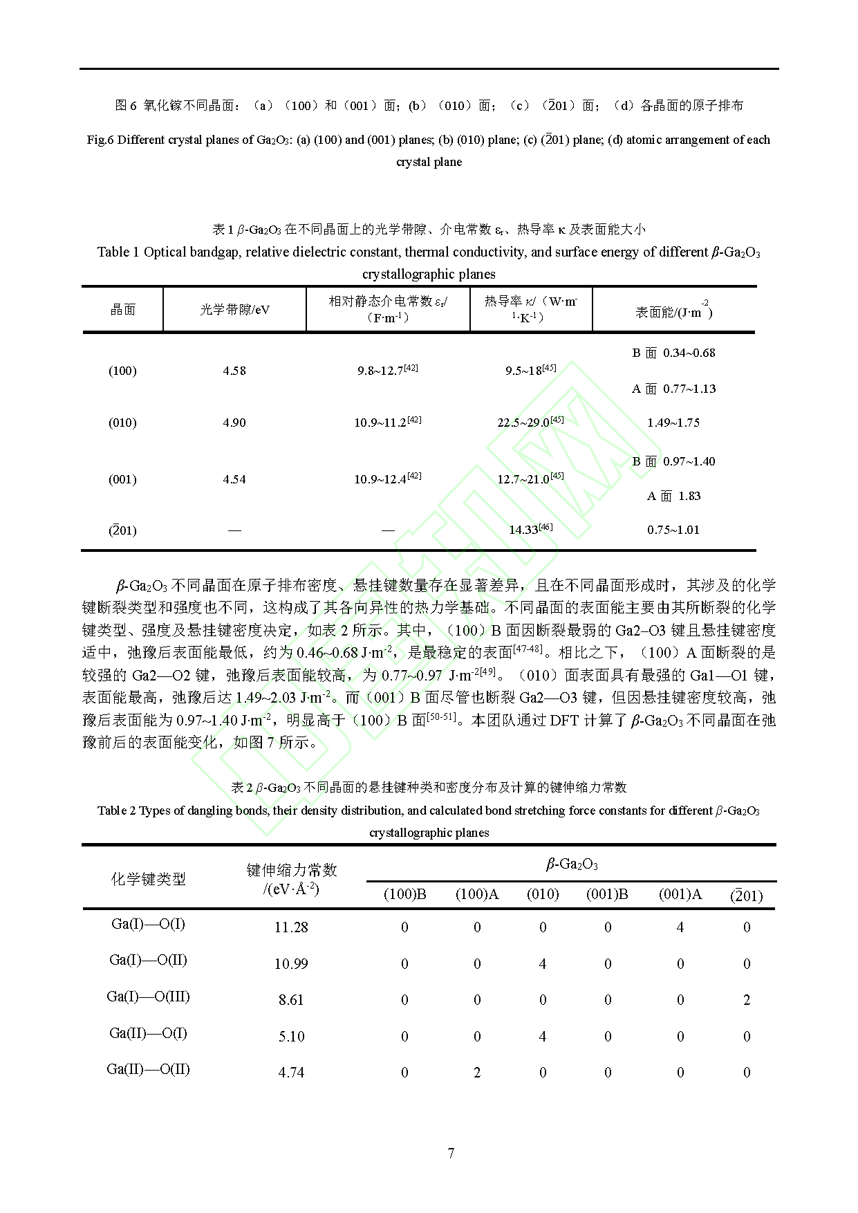
Fig.6 Different crystal planes of Ga2O3: (a) (100) and (001) planes; (b) (010) plane; (c) (-201) plane; (d) atomic arrangement of each crystal plane
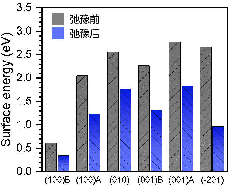
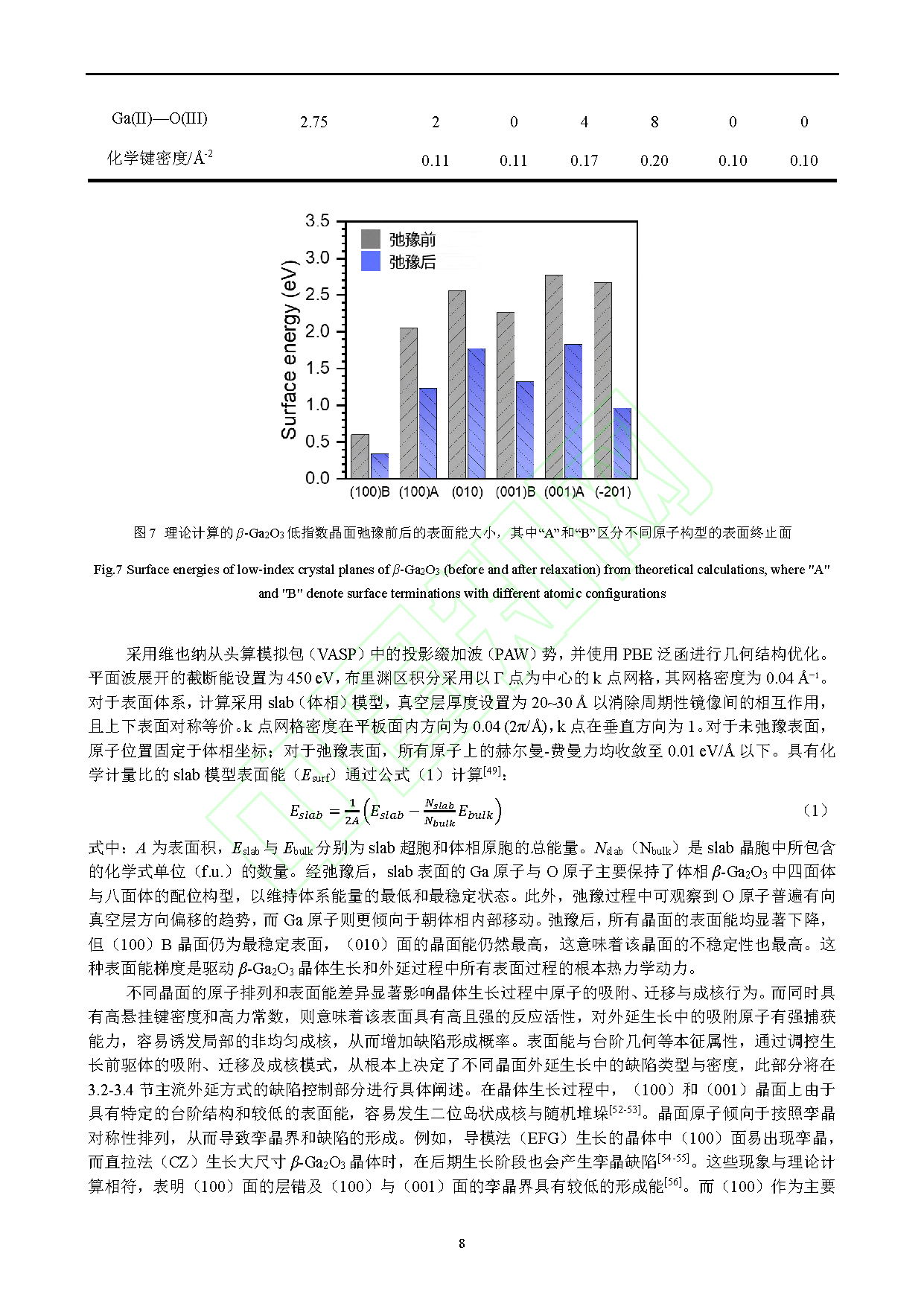
Fig.7 Surface energies of low-index crystal planes of β-Ga2O3 (before and after relaxation) from theoretical calculations, where "A" and "B" denote surface terminations with different atomic configurations
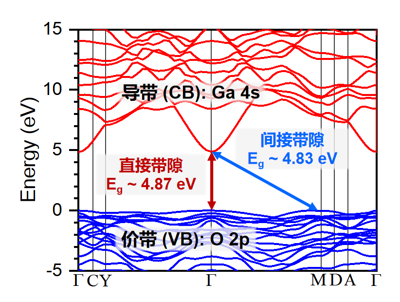
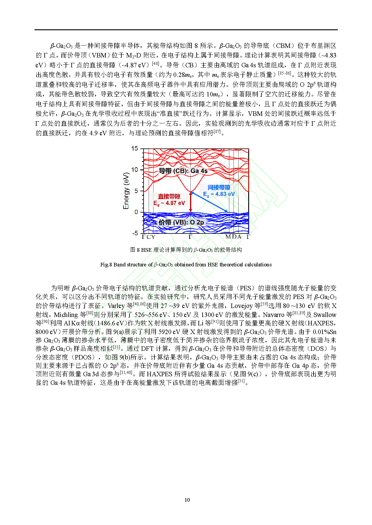
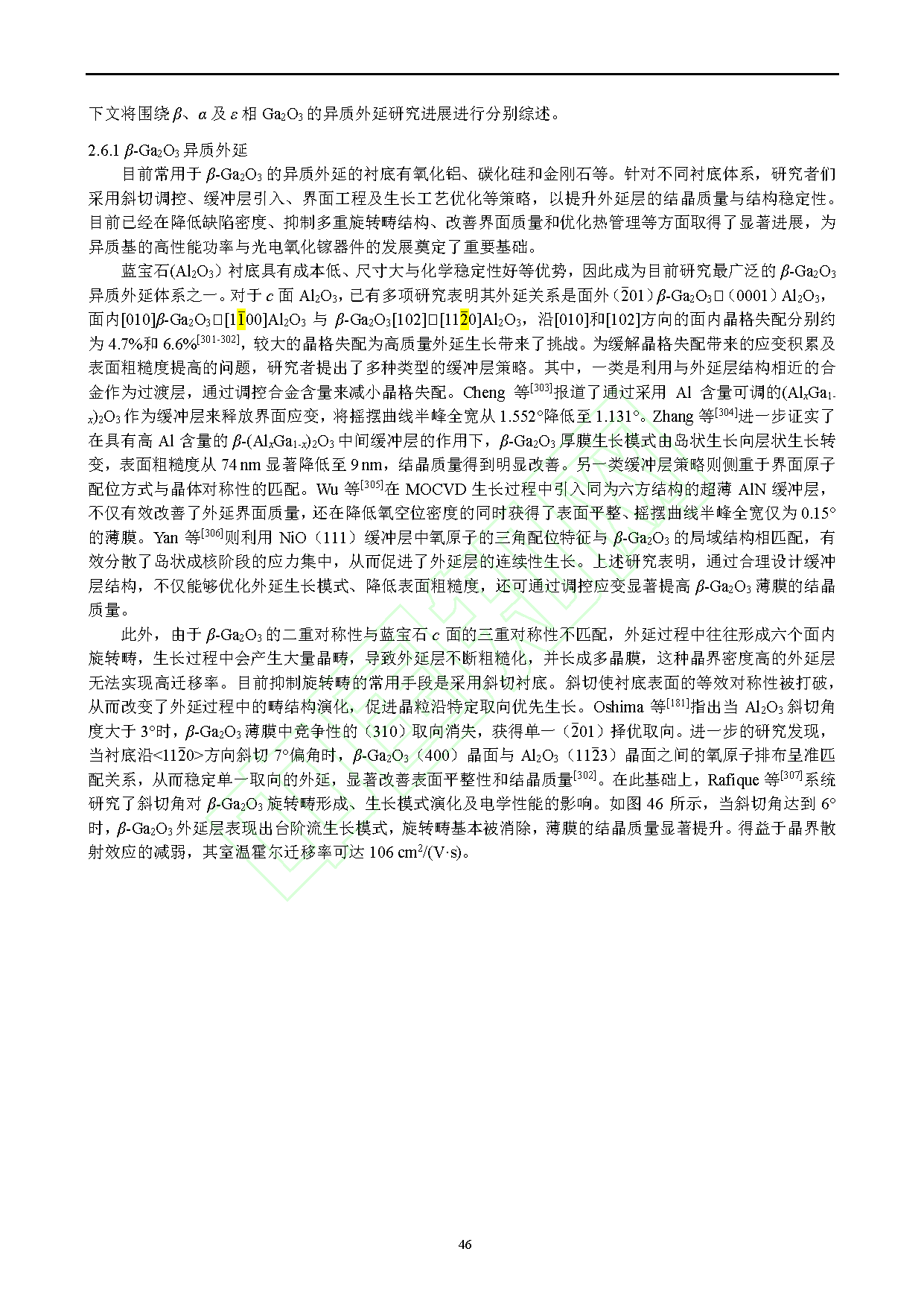
Fig.8 Band structure of β-Ga2O3 obtained from HSE theoretical calculations
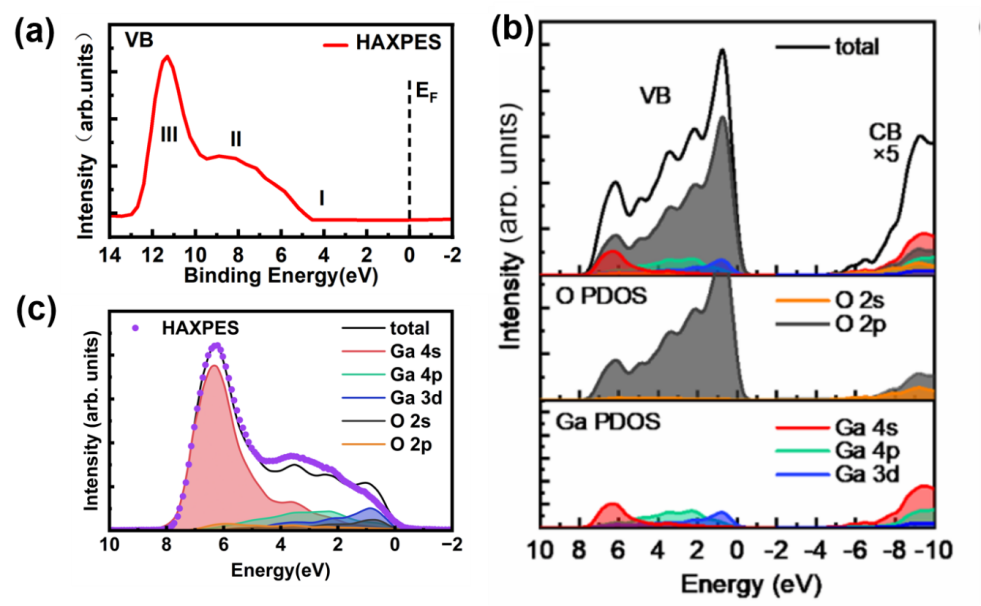
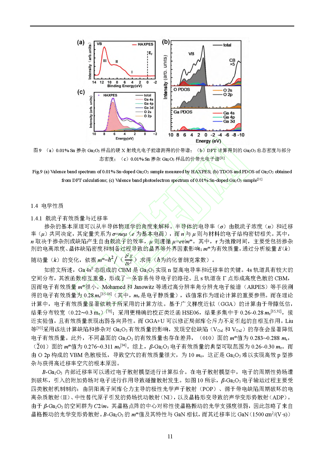
Fig.9 (a) Valence band spectrum of 0.01% Sn-doped Ga2O3 sample measured by HAXPES; (b) TDOS and PDOS of Ga2O3 obtained from DFT calculations; (c) Valence band photoelectron spectrum of 0.01% Sn-doped Ga₂O₃ sample
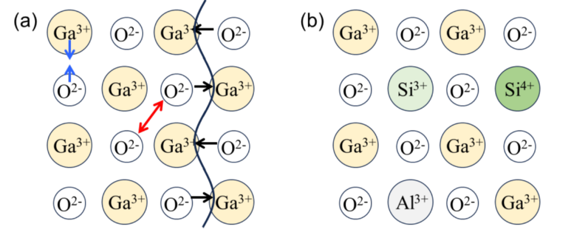
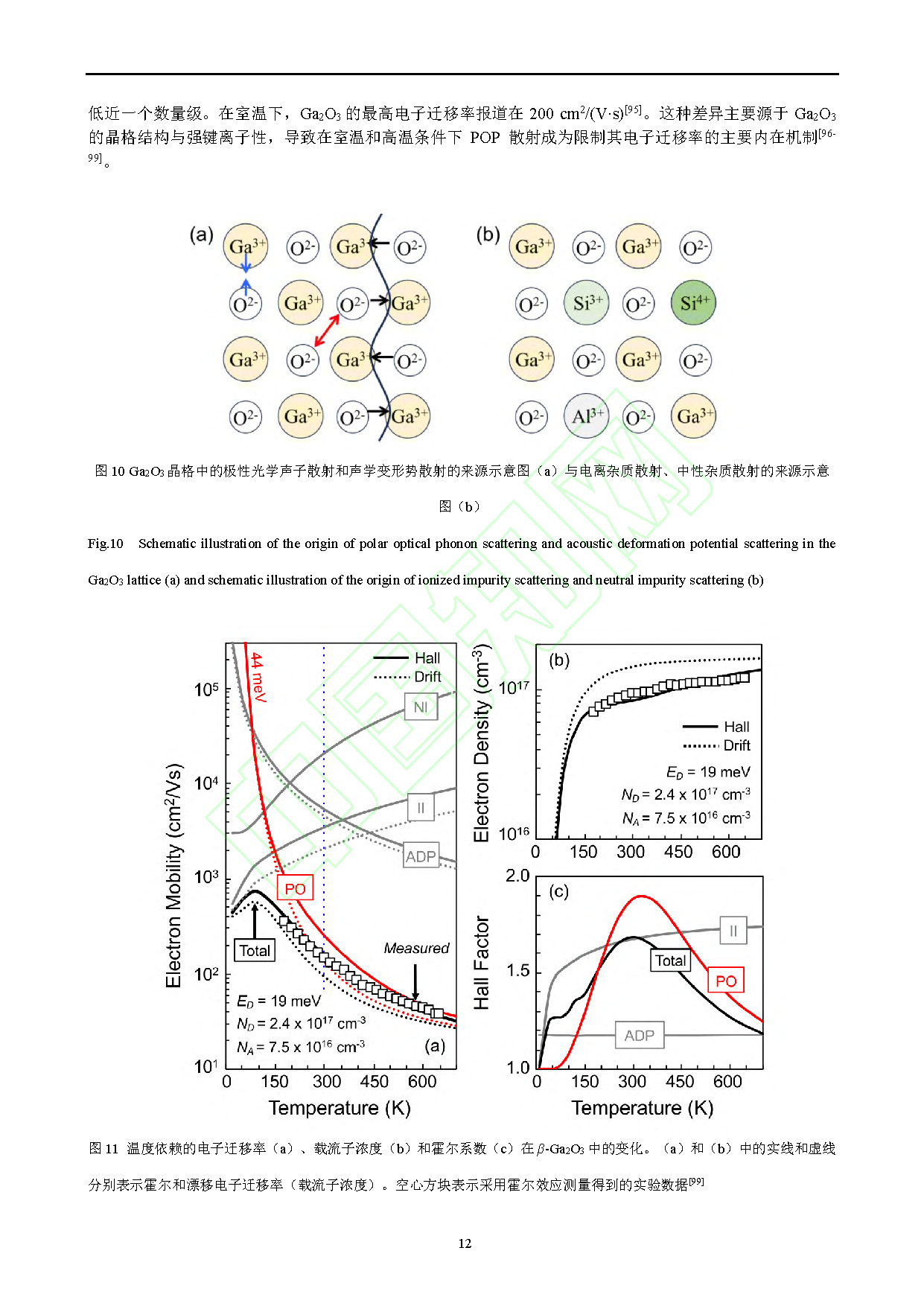
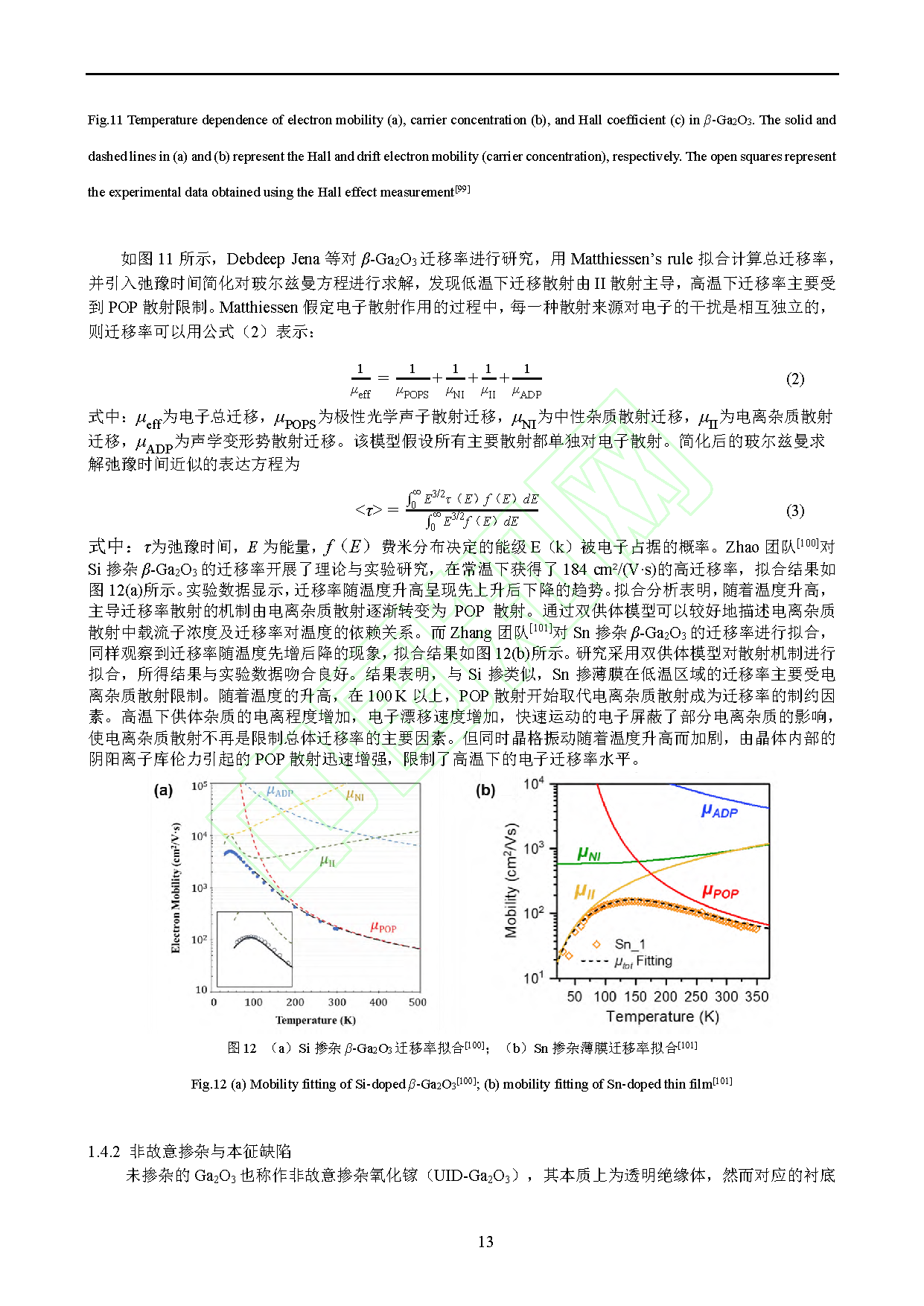
Fig.10 Schematic illustration of the origin of polar optical phonon scattering and acoustic deformation potential scattering in the Ga2O3 lattice (a) and schematic illustration of the origin of ionized impurity scattering and neutral impurity scattering (b)
知网链接:
https://kns.cnki.net/kcms2/article/abstract?v=Omth-A4cfW9hvu8wLxsdYbpZStb_aISwhEtFtFjxadu5N15Rg1izqI5GsADCFgbVCqM1TJu6Okcki7MRAWxmudIgccTxaIYPHDGDgBqdLUDBn7rrtojYw7iZe7vNhcltzNmk9iu49Nh3M0mOe7vNnF5skXlyNWaprC2kP-Si_Kxw9TPCCo2QxA==&uniplatform=NZKPT&language=CHS