Paper Sharing
【Domestic Papers】Synergy of fluorine-based plasma treatment and wet chemical treatment for β-Ga₂O₃ Schottky barrier diode (SBD) with superior breakdown characteristics
日期:2026-04-27阅读:172
Researchers from Hefei University of Technology have published a dissertation titled “Synergy of fluorine-based plasma treatment and wet chemical treatment for β‑Ga₂O₃ Schottky barrier diode (SBD) with superior breakdown characteristics” in Applied Surface Science.
Background
β‑Ga₂O₃ is an ideal candidate for next-generation power devices as an ultra-wide bandgap semiconductor, owing to its high critical electric field and excellent Baliga’s figure of merit. In device fabrication, dry processes such as ICP etching tend to introduce lattice damage and oxygen vacancy defects, leading to increased leakage current and reduced breakdown voltage. Traditional post-etch repair strategies can hardly achieve both surface planarization and efficient defect passivation simultaneously. Fluorine-based plasma can realize surface doping and passivation, but tends to leave a damaged layer. The synergistic regulation mechanism with wet treatments such as hot phosphoric acid and TMAH is still unclear, and there is a lack of an integrated process scheme that balances low on-resistance and high breakdown voltage.
Abstract
In this work, we demonstrate an effective strategy for enhancing the performance of β‑Ga₂O₃ Schottky barrier diodes (SBDs) through synergistic fluorine-based inductively coupled plasma (ICP) treatment and post-wet chemical processing. An SF₆/Ar gas mixture (18/2 sccm) was employed for anode plasma treatment prior to electrode deposition, yielding a smooth surface morphology with root mean square (RMS) roughness of 0.179 nm. The fluorine-based plasma treatment introduces shallow donor-like doping near the surface and passivates dangling bonds, reducing the specific on-resistance (Rₒₙ,ₛₚ) from 4.25 to 2.61 mΩ·cm² and increasing the reverse breakdown voltage (BV) from 530 V to 560 V. A post-wet chemical treatment with hot H₃PO₄ further boosts the BV to 770 V by passivating the plasma-induced defects. Although the H₃PO₄-treatment leads to a slight increase in Rₒₙ,ₛₚ, the power figure-of-merit (PFOM) is significantly enhanced from 62.98 to 154.4 MW·cm⁻². This work establishes a viable pathway toward β‑Ga₂O₃ SBDs with superior breakdown characteristics.
Highlights
Synergistic fluorine-based ICP treatment and hot H₃PO₄ wet chemical treatment for high-performance β‑Ga₂O₃ SBDs.
SF₆/Ar plasma treatment achieves smooth surface with RMS roughness of 0.179 nm and reduces Rₒₙ,ₛₚ to 2.61 mΩ・cm².
Hot H₃PO₄ treatment passivates plasma damage and boosts breakdown voltage to 770 V.
Power figure-of-merit (PFOM) significantly improved from 62.98 to 154.4 MW・cm⁻².
Effective strategy for balancing on-resistance and breakdown characteristics in β‑Ga₂O₃ power devices.
Conclusion
In summary, an SF₆/Ar gas mixture was adopted for the anode plasma treatment before electrode deposition of β‑Ga₂O₃ SBDs. At an SF₆/Ar flow ratio of 18/2, the etching process exhibits a moderate etch rate and yields a smooth surface morphology, thereby providing favorable conditions for the fabrication of high-quality SBDs. Following the fluorine-based plasma treatment, Rₒₙ,ₛₚ of the device was reduced from 4.25 to 2.61 mΩ·cm² and BV was improved from 530 to 560 V, which should be attributed to shallow donor-like fluorine doping in the near surface and the passivation effect of fluorine. A post-wet chemical treatment with hot H₃PO₄ can further improve the BV to 770 V by passivating the plasma-damaged layer. Despite the increased Rₒₙ,ₛₚ, PFOM of the device was improved from 62.98 MW·cm⁻² to 154.4 MW·cm⁻². Synergy of fluorine-based plasma treatment and wet chemical treatment presents to be an effective strategy for the fabrication of β‑Ga₂O₃ SBDs with minimal etching-induced damage and high breakdown voltage.
Project Support
This work was supported by the National Natural Science Foundation of China (NSFC, No. 62074048), the Key Research and Development Plan of Anhui Province (No. 2022f04020007), and the Natural Science Foundation of Anhui Province (No. 2208085MF177).
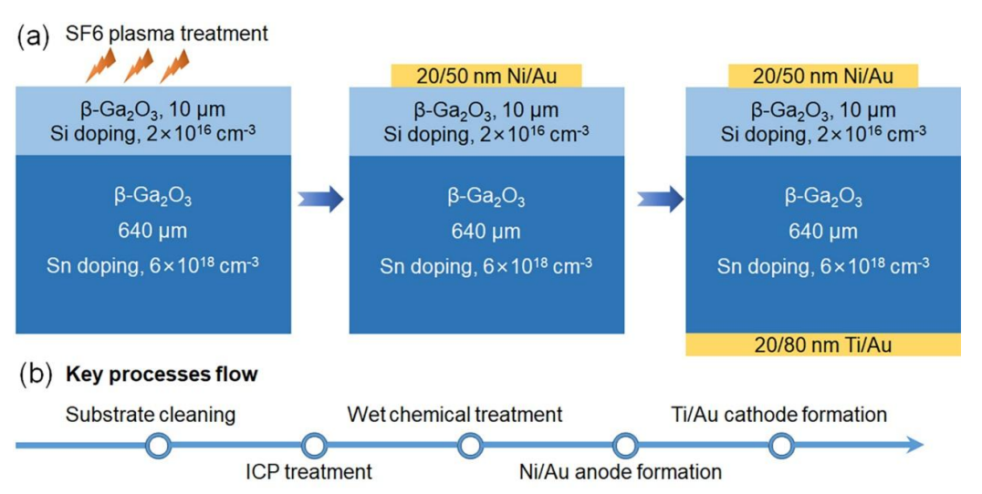
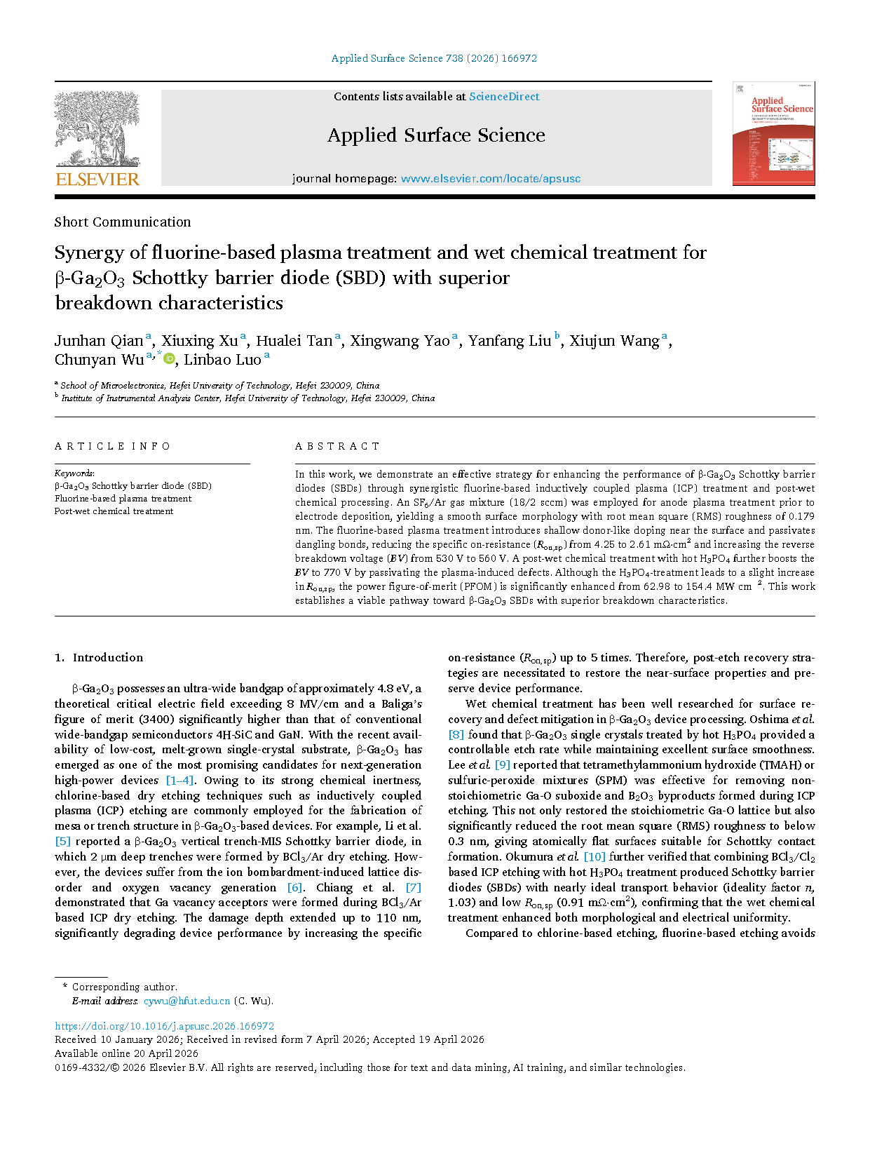
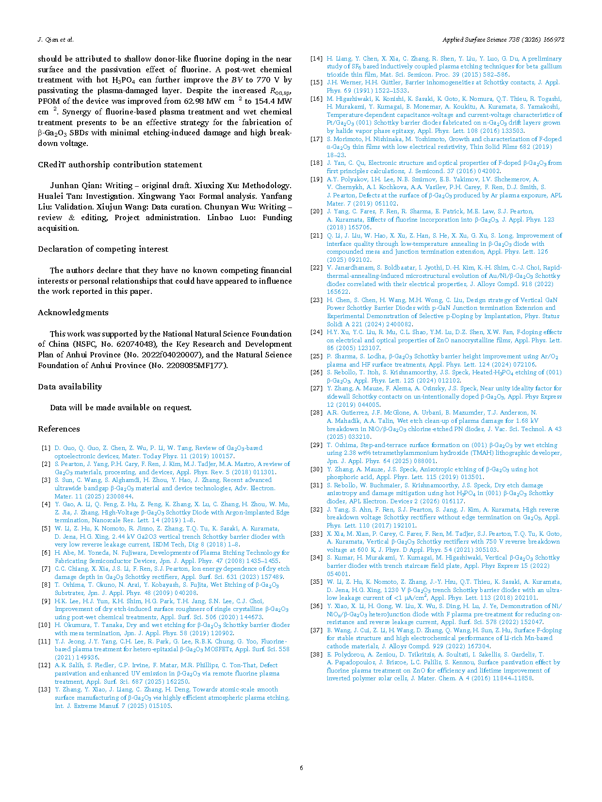
Fig. 1. (a) Cross-sectional schematic and (b) the fabrication process flow of the vertical β‑Ga₂O₃ SBD.
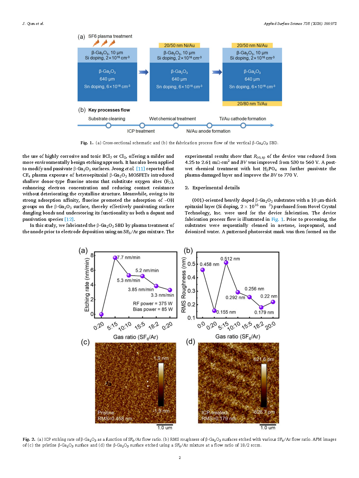
Fig. 2. (a) ICP etching rate of β‑Ga₂O₃ as a function of SF₆/Ar flow ratio. (b) RMS roughness of β‑Ga₂O₃ surfaces etched with various SF₆/Ar flow ratio. AFM images of (c) the pristine β‑Ga₂O₃ surface and (d) the β‑Ga₂O₃ surface etched using a SF₆/Ar mixture at a flow ratio of 18/2 sccm.
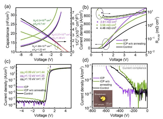
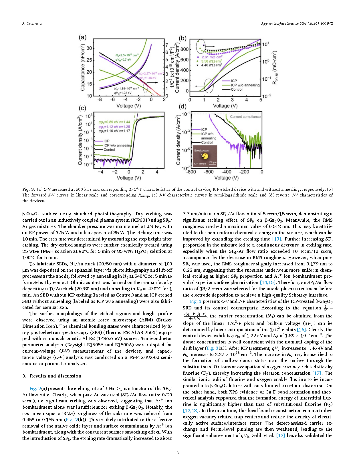
Fig. 3. (a) C–V measured at 500 kHz and corresponding 1/C²–V characteristics of the control device, ICP etched device with and without annealing, respectively. (b) The forward J–V curves in linear scale and corresponding Rₒₙ,ₛₚ, (c) J–V characteristic curves in semi-logarithmic scale and (d) reverse J–V characteristics of the devices.
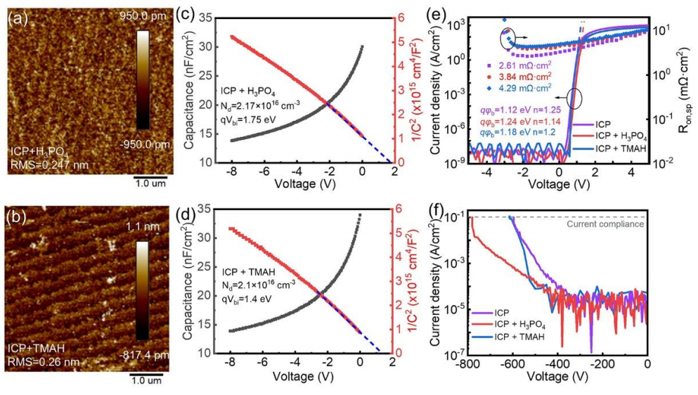
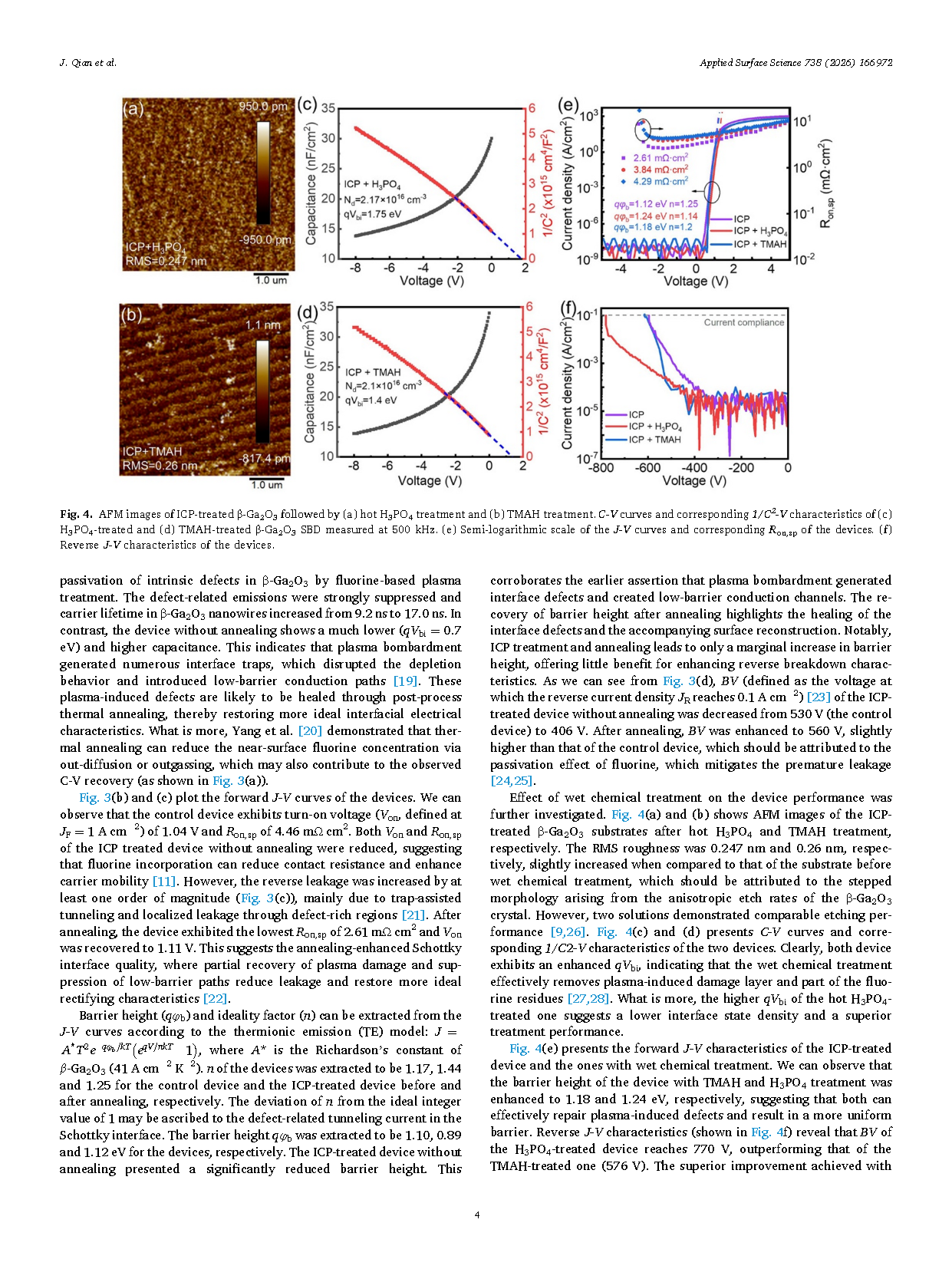
Fig. 4. AFM images of ICP-treated β‑Ga₂O₃ followed by (a) hot H₃PO₄ treatment and (b) TMAH treatment. C–V curves and corresponding 1/C²–V characteristics of (c) H₃PO₄-treated and (d) TMAH-treated β‑Ga₂O₃ SBD measured at 500 kHz. (e) Semi-logarithmic scale of the J–V curves and corresponding Rₒₙ,ₛₚ of the devices. (f) Reverse J–V characteristics of the devices.
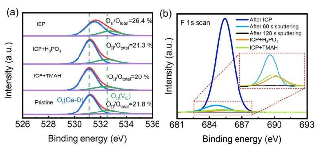
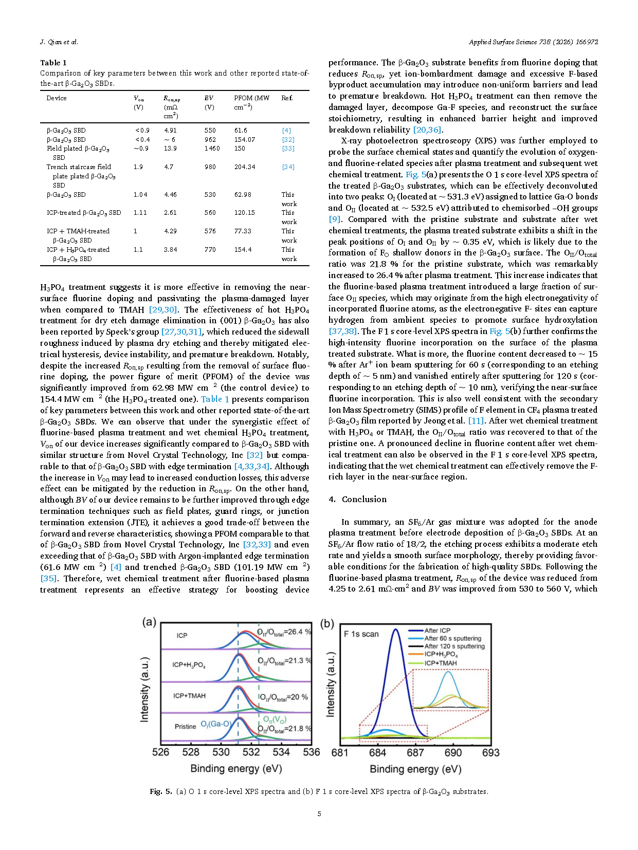
Fig. 5. (a) O 1s core-level XPS spectra and (b) F 1s core-level XPS spectra of β‑Ga₂O₃ substrates.
DOI:
doi.org/10.1016/j.apsusc.2026.166972