Paper Sharing
【Member Papers】Ultrawide Bandgap Semiconductor in Photonic Devices: From Fundamental Nonlinear Optical Properties to Emerging Devices
日期:2026-04-28阅读:165
Researchers from the Suzhou University of Technology have published a dissertation titled "Ultrawide Bandgap Semiconductor in Photonic Devices: From Fundamental Nonlinear Optical Properties to Emerging Devices" in Chinese Journal of Lasers.
Background
The rapid development of artificial intelligence technology has placed extremely high demands on computing power and network communication bandwidth. Against this backdrop, photonic integrated circuits (PICs) have emerged as a key technology to replace traditional electronic integrated circuits, thanks to their advantages of high speed, high parallelism, and low power consumption. Although silicon-based photonics is currently at the core, it is limited by the narrow bandgap of silicon material at approximately 1.1 eV, with a transparency window covering only the 1.1-8.5 μm band. This makes it difficult to meet the application requirements of quantum optics, precision spectroscopy, virtual reality, atomic clocks, etc., which need ultraviolet-visible or mid-infrared bands. To fill the spectral gap, the academic community has explored various materials, but so far, no single material can independently perform all functions of light generation, modulation, transmission, and detection. Therefore, heterogeneous integration of multiple materials has become the preferred solution for high-performance chips. Ultra-wide bandgap semiconductors represented by gallium oxide (Ga2O3), aluminum nitride (AlN), and diamond (Diamond), with their extremely wide transparency windows, rich nonlinear optical effects, high refractive index contrast, and good process compatibility, have become ideal platforms for developing integrated devices in the ultraviolet-visible or mid-infrared bands. These materials play an irreplaceable role in core devices such as supercontinuum generation, optical frequency combs, electro-optic modulation, and micro-nano lasers, and are the foundation for realizing "CMOS+X" hybrid integrated optoelectronic devices.
Abstract
Significance The rapid development of artificial intelligence (AI), high-speed communication network and Internet of Things (IoT) has introduced unprecedented demands on computing power and network bandwidth. However, electronic integrated circuits have reached a bottleneck due to the slowdown of Moore’s law. In the last two decades, photonic integrated circuits (PICs) have gained significant attention worldwide due to their unique advantages such as high speed, multi-domain parallelism capability, low power consumption, etc. As a result, PICs have been regarded as a potential replacement to traditional electronic integrated circuits in the “post-Moore era.” Currently, silicon photonics holds the dominant position in the development of PICs, which is attributed to the high integration density, mature fabrication procedure and compatibility with complementary metal-oxide-semiconductor (CMOS) technology. However, limited by the bandgap of silicon semiconductor (~1.1 eV), the transparent window of silicon photonics only covers the 1.1~8.5 µm wavelength range. This makes it difficult to meet the growing demands of applications requiring ultraviolet-visible or mid-infrared light, such as quantum optics, precision spectroscopy, AR/VR virtual reality displays, atomic clocks, optical computing, and remote sensing. Therefore, high-performance optical materials are essential for the development of PIC technology. In recent years, ultra-wide bandgap (UWBG) semiconductors have emerged as candidate photonic materials in PIC devices due to their broad transparent windows, rich nonlinear optical effects, high refractive index contrast, and good stability. By integrating UWBG semiconductors with existing silicon photonic platforms (CMOS+X), various optical functionalities, including photodetection, optical modulation, waveguide and on-chip nonlinear optical processes, can be realized on integrated platform. Research on the nonlinear optical response and integrated photonic structures of UWBG semiconductors not only shed new light on fundamental semiconductor physics but also paving the way for future heterogeneous integrated PIC devices.
Conclusion
In summary, UWBG semiconductors Ga₂O₃, AlN and diamond have emerged as promising candidates in nonlinear optics and PICs. Heterogeneous integration of UWBG semiconductors with silicon platforms "CMOS+X" can significantly improve the performance of photonic integrated devices by making full use of the advantages of various materials. However, several issues remain to be addressed. We believe the progress on advanced manufacturing, nano fabrication, optical characterization and heterogeneous integration technology will drive the future development of UWBG semiconductors in optics.
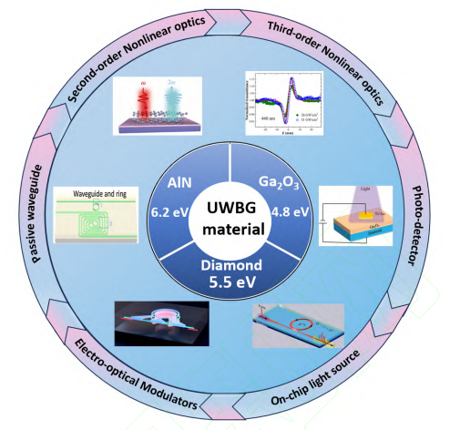
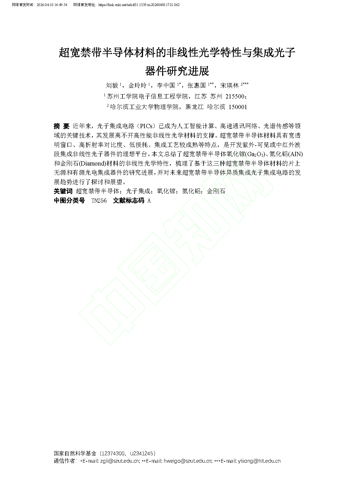
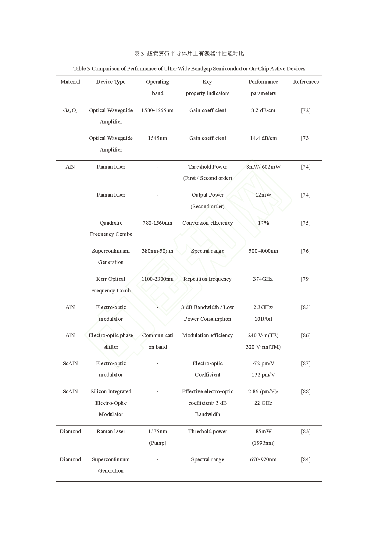
Fig. 1 Schematic diagram of ultrawide bandgap (UWBG) semiconductors in nonlinear optics and integrated photonics
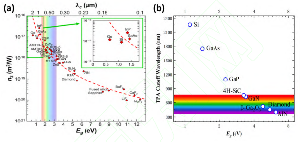
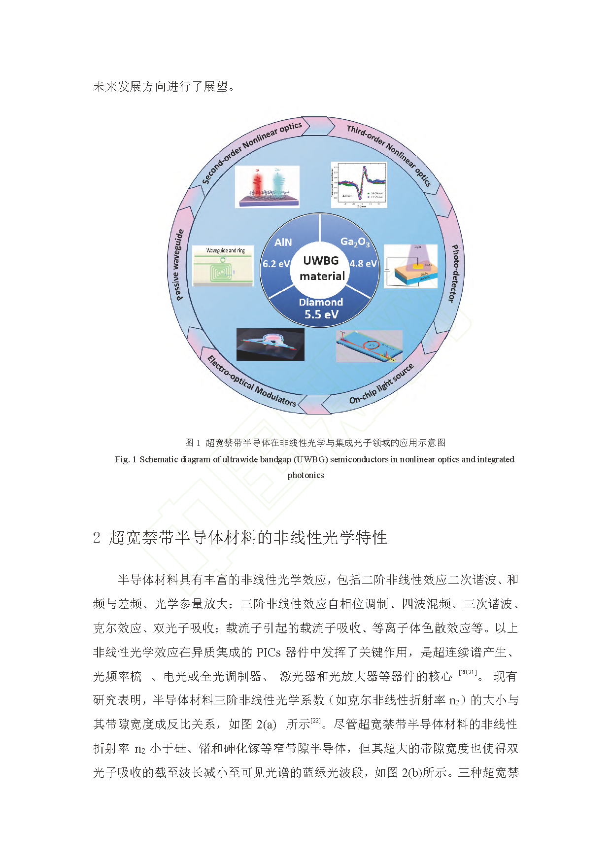
Fig. 2(a) Dependence of the nonlinear refractive index n2 of 30 materials on their band gap; (b) Cutoff wavelengths of Two-Photon Absorption (TPA) plotted versus bandgap energies of various semiconductor materials
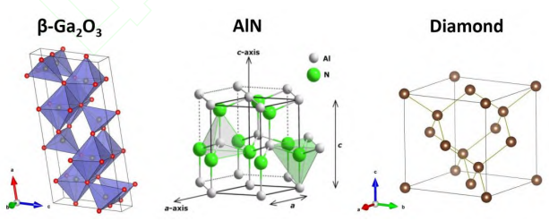
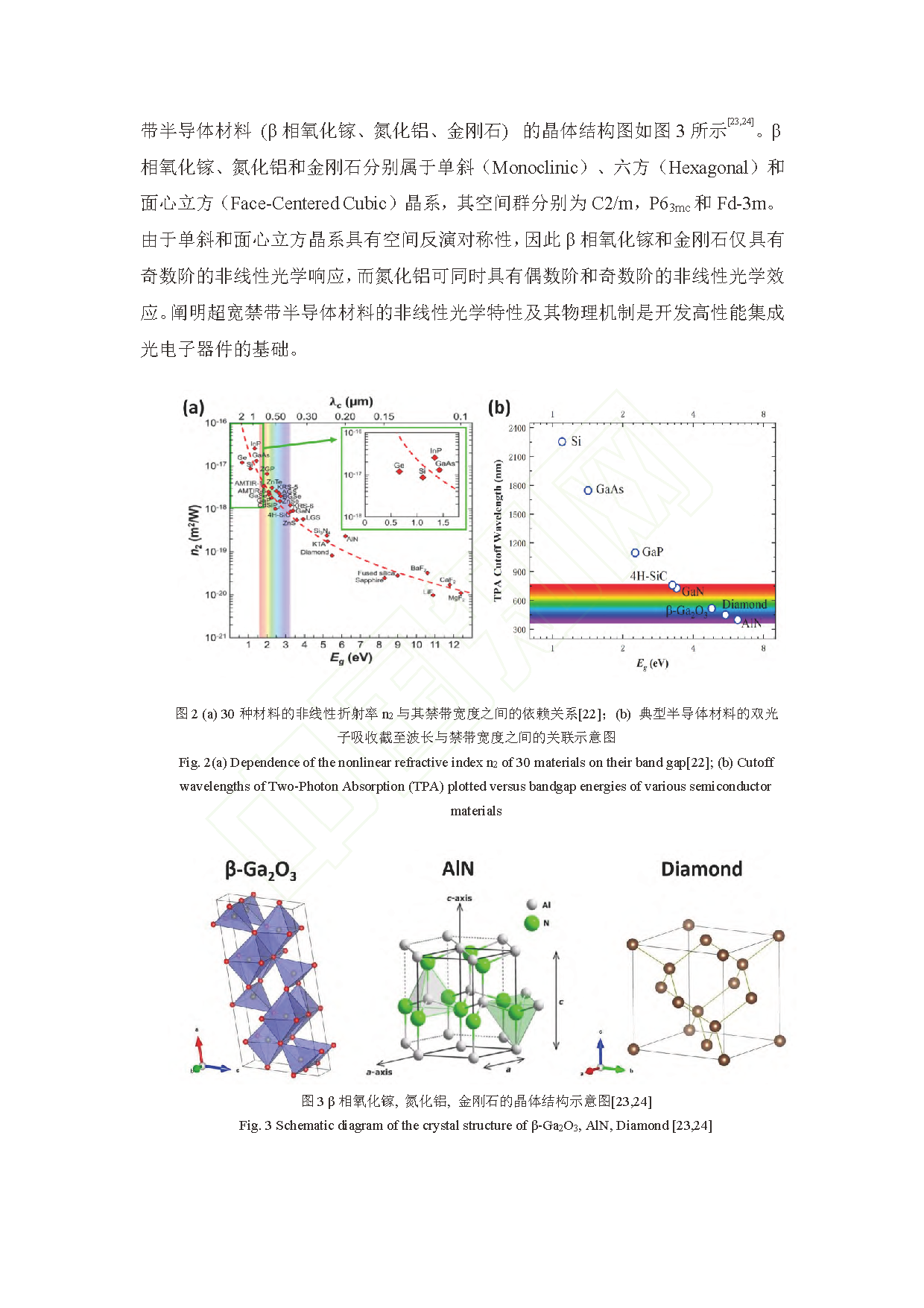
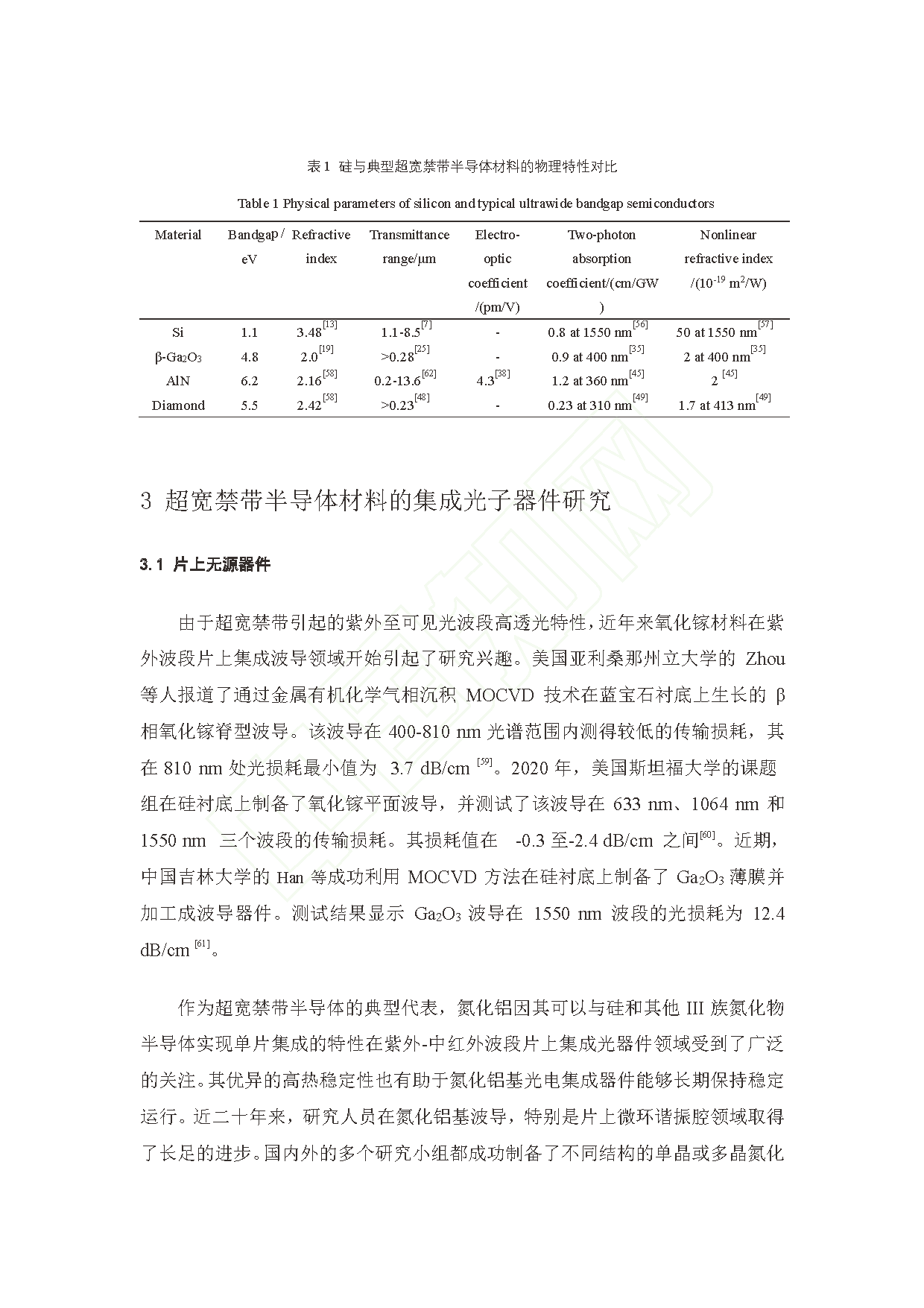
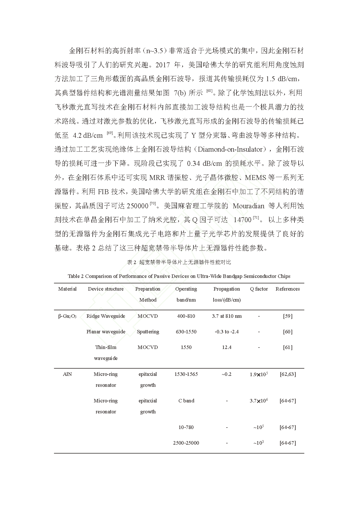
Fig. 3 Schematic diagram of the crystal structure of β-Ga2O3, AlN, Diamond
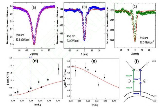
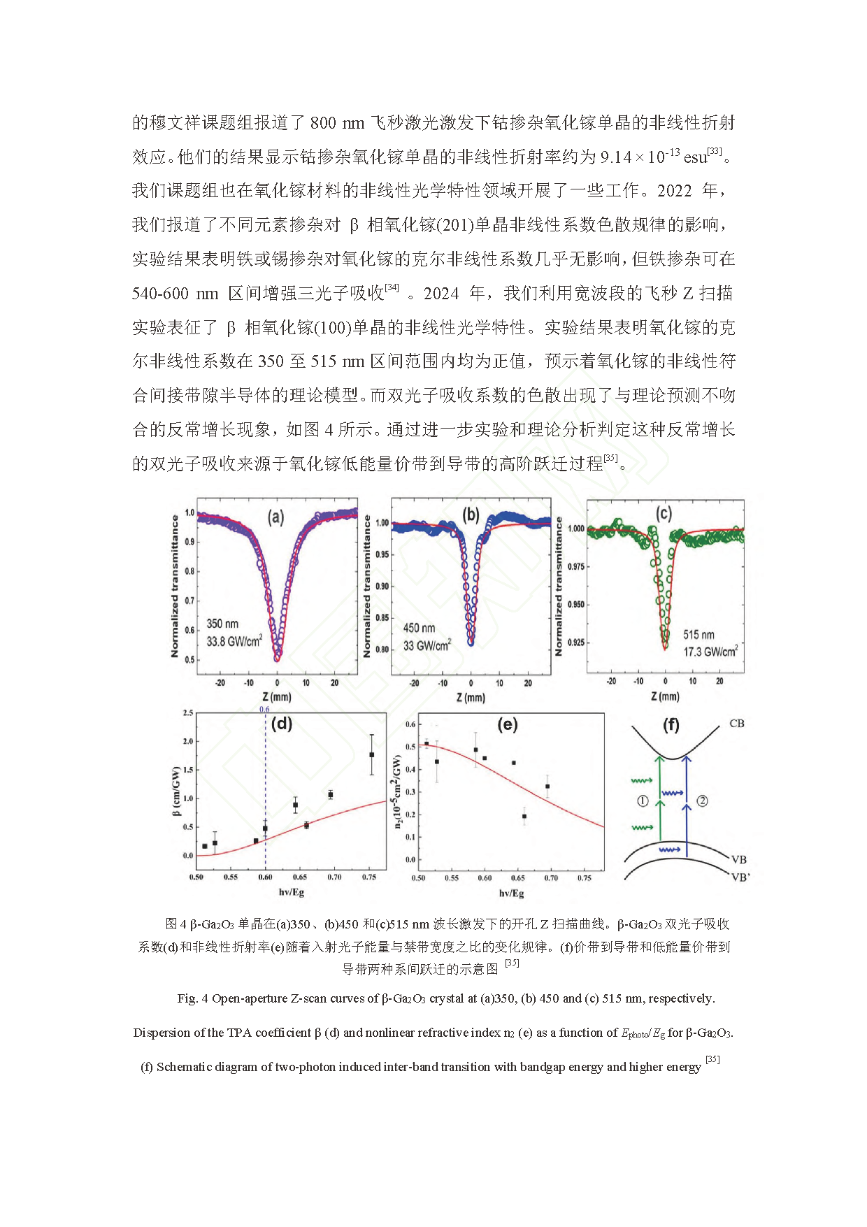
Fig. 4 Open-aperture Z-scan curves of β-Ga2O3 crystal at (a)350, (b) 450 and (c) 515 nm, respectively. Dispersion of the TPA coefficient β (d) and nonlinear refractive index n2 (e) as a function of Ephoto/Eg for β-Ga2O3. (f) Schematic diagram of two-photon induced inter-band transition with bandgap energy and higher energy
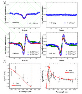
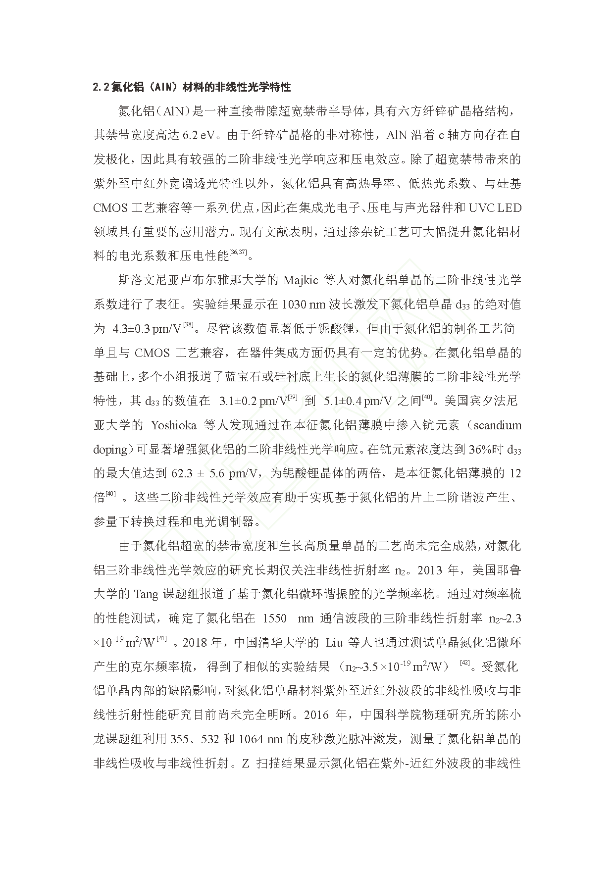
Fig. 5 (a) Open-aperture and closed-aperture Z-scan curves of the AlN crystal under 400 and 440 nm laser excitation. (b) Dispersion of the TPA coefficient β and nonlinear refractive index n2 as a function of Ephoto/Eg for AlN
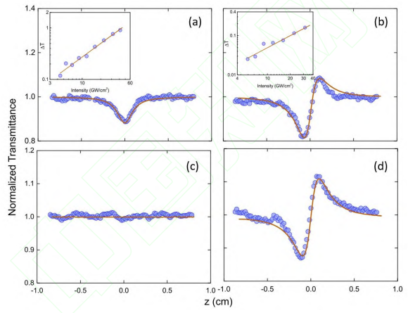
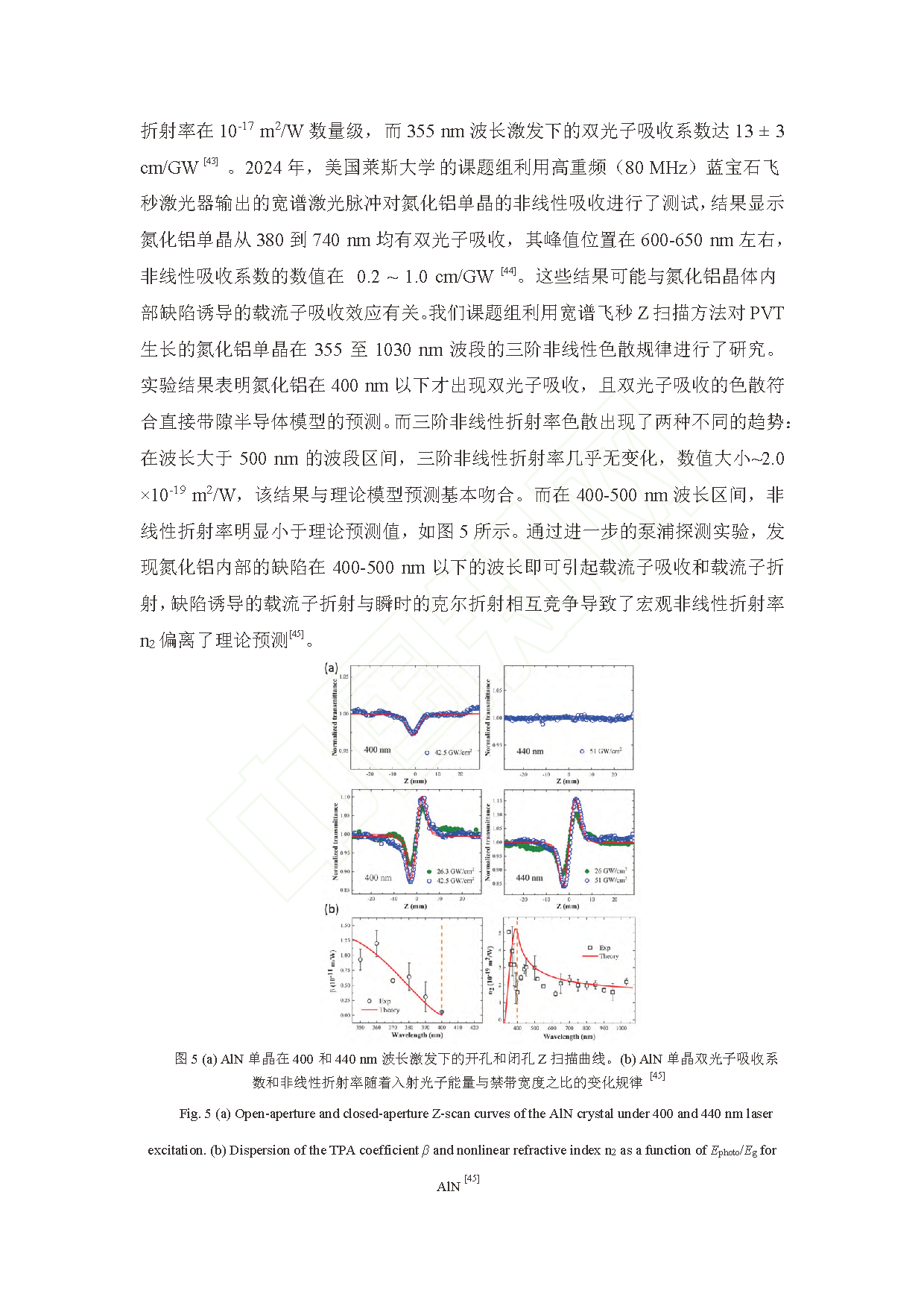
Fig. 6 Open and closed-aperture Z-scan curves of diamond crystal at 3.54 eV (350 nm) (a and b, respectively) and 2.21 eV (560 nm) (c and d, respectively)
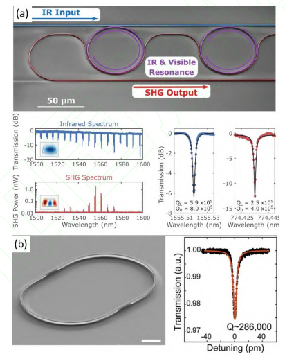
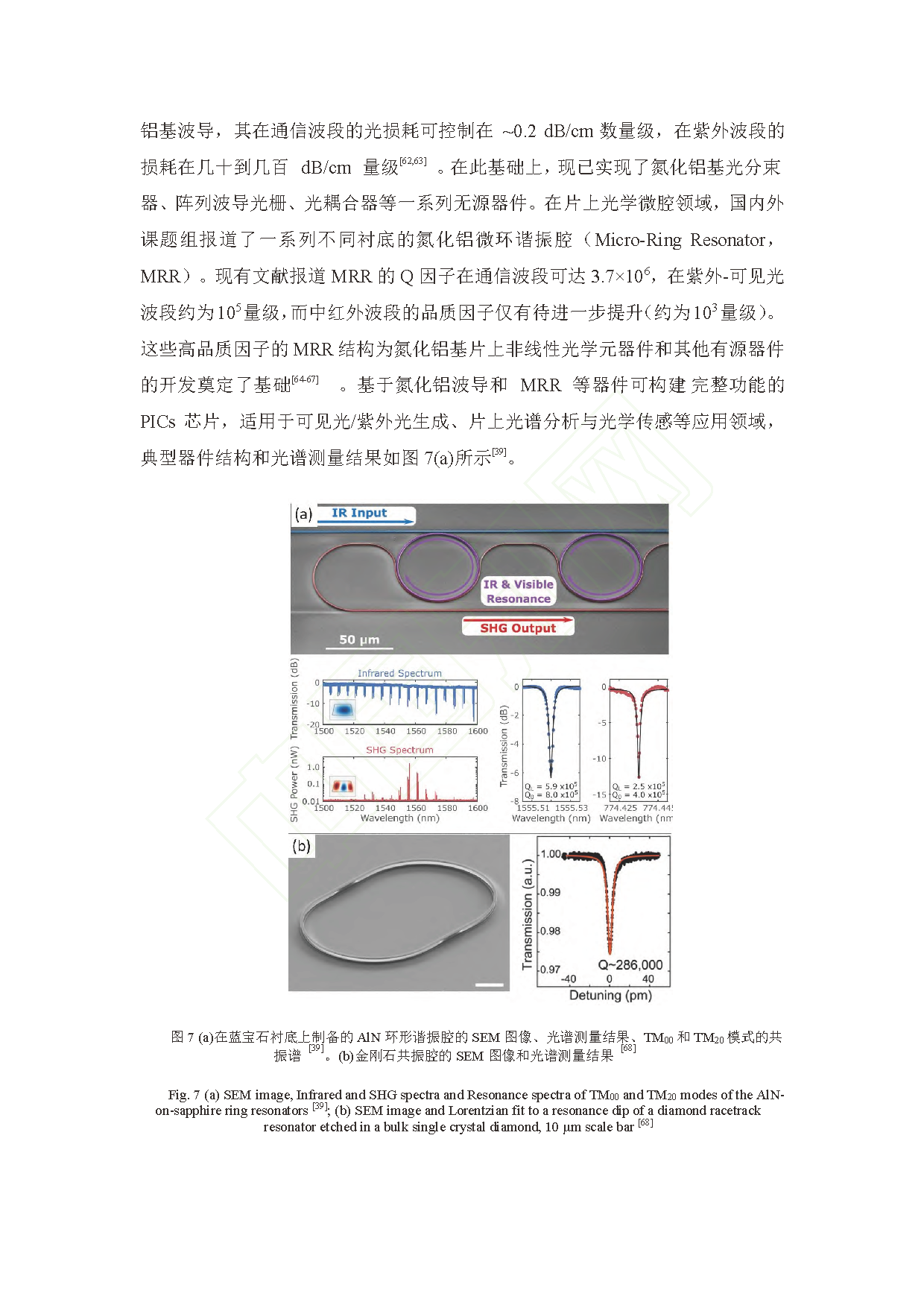
Fig. 7 (a) SEM image, Infrared and SHG spectra and Resonance spectra of TM00 and TM20 modes of the AlNon-sapphire ring resonators; (b) SEM image and Lorentzian fit to a resonance dip of a diamond racetrack resonator etched in a bulk single crystal diamond, 10 μm scale bar
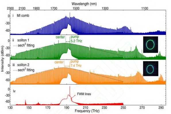
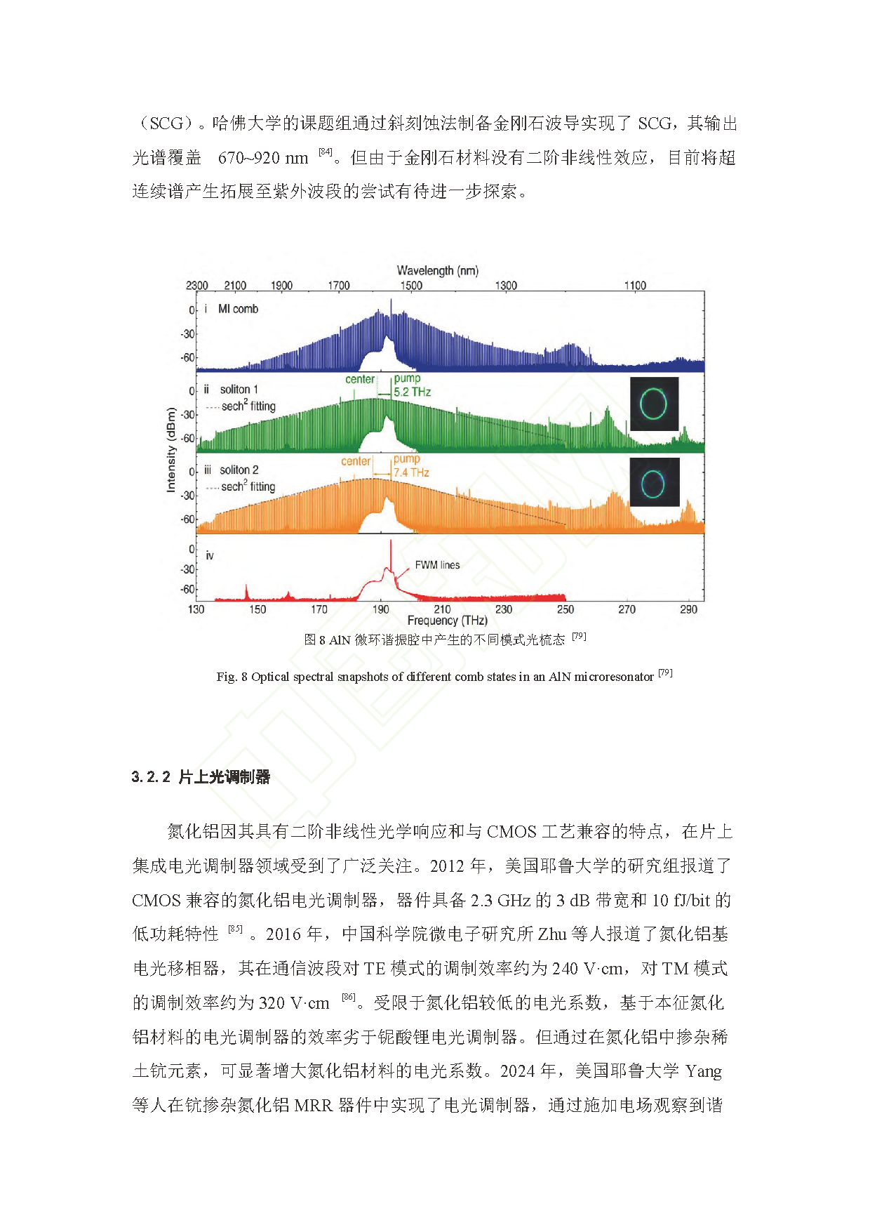
Fig. 8 Optical spectral snapshots of different comb states in an AlN microresonator
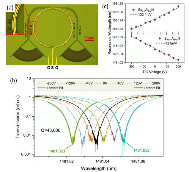
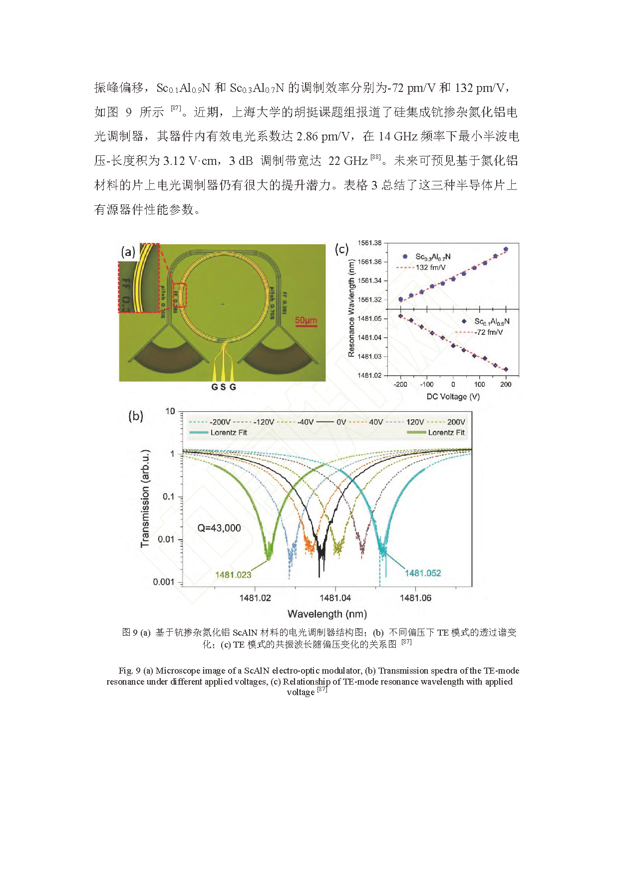
Fig. 9 (a) Microscope image of a ScAlN electro-optic modulator, (b) Transmission spectra of the TE-mode resonance under different applied voltages, (c) Relationship of TE-mode resonance wavelength with applied voltage
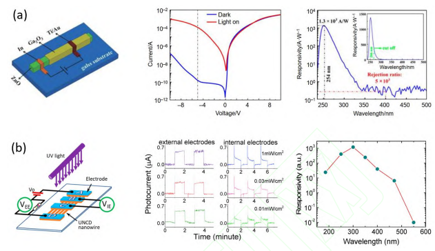
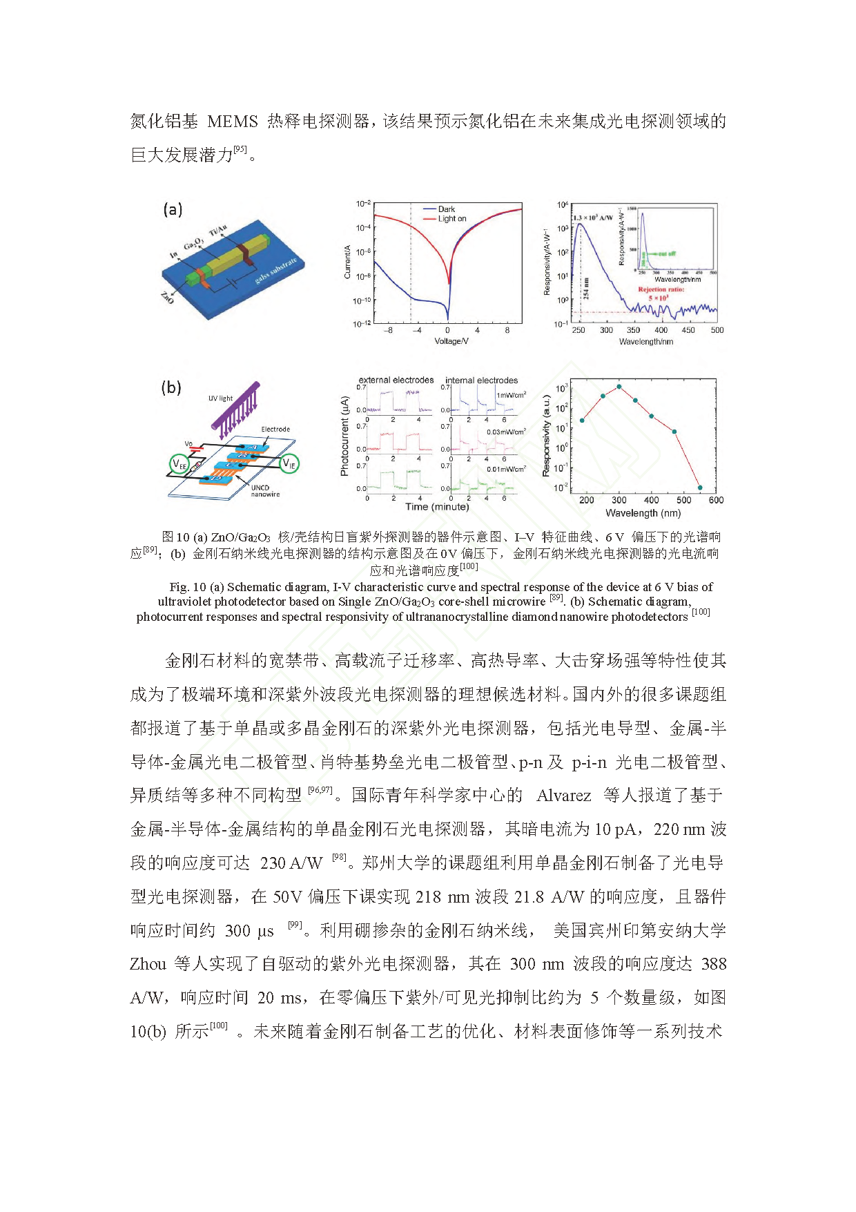
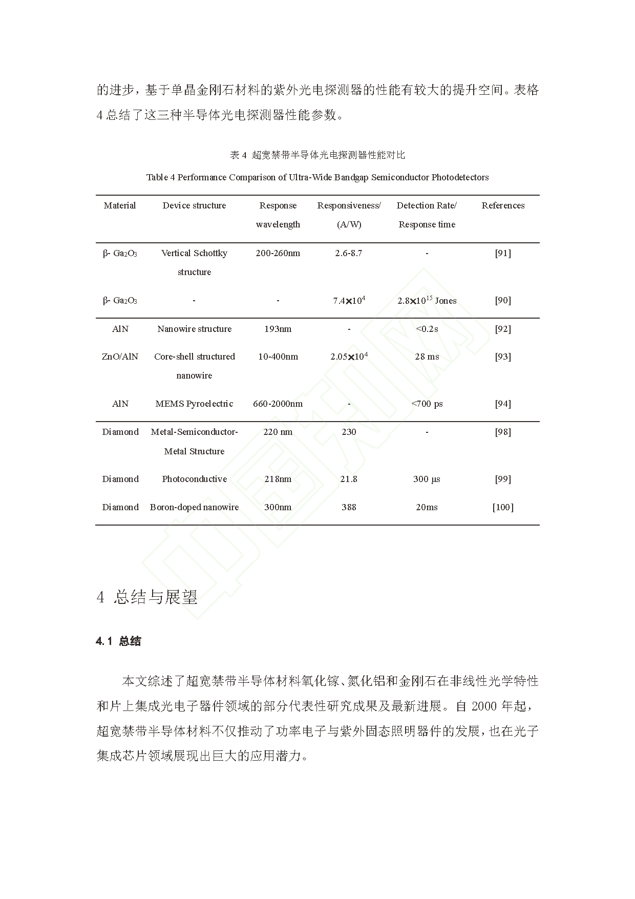
Fig. 10 (a) Schematic diagram, I-V characteristic curve and spectral response of the device at 6 V bias of ultraviolet photodetector based on Single ZnO/Ga2O3 core-shell microwire. (b) Schematic diagram, photocurrent responses and spectral responsivity of ultrananocrystalline diamond nanowire photodetectors
LINK:
https://kns.cnki.net/kcms2/article/abstract?v=JRmhR0Lfi27YOVyDgFMGnk5Me58LQDzxCI5Iaab0hqwsl8hZHRkbMVVQTxwNoT8eAKod4ZQ4nImMQ6ALvmqMj5cA4YSRbzlBq8zfPiYz66xz5MuGH5yH2J6jfupfnr1cVHbDCxQc3sItLGY1BGcrwtpEjdkGlIeVcn7855NxRlto94Y8soyGYQ==&uniplatform=NZKPT&language=CHS