Paper Sharing
【Member Papers】 Beyond a single mechanism: Uncovering the dual origin of degradation in β-Ga₂O₃ SBDs under forward bias stress
日期:2026-04-28阅读:219
Researchers from Xidian University have published a dissertation titled " Beyond a single mechanism: Uncovering the dual origin of degradation in β-Ga2O3 SBDs under forward bias stress" in Applied Physics Letters.
Background
β-gallium oxide (β-Ga2O3) is emerging as a highly promising material for next-generation power electronics due to its ultra-wide bandgap and exceptional Baliga’s figure of merit (BFOM). Fundamental to this development is the β-Ga2O3 Schottky barrier diode (SBD), an essential component in high-efficiency rectifiers and power converters. Although advanced structures such as field plates have markedly improved the performance of SBDs, the long-term reliability of such devices has not been clarified. Specifically, their stability under prolonged forward conduction—the most common operating mode involving high currents and severe self-heating effects— remains poorly understood.
Abstract
This study delineated the degradation of β-Ga2O3 Schottky barrier diodes under forward bias stress and identified the physical cause of performance instability in these diodes. Stress was found to increase the reverse leakage current and the forward current under low biases and decrease the turn-on voltage. The values of these parameters were partially recovered after annealing. The increased noise power spectral density after stress application was completely recovered after annealing, indicating that device degradation caused by interface defects is reversible. From the temperature-dependent low-frequency noise results, the interface defect energy levels were determined to be about EC - 0.35 eV (EC = conduction band minimum). Deep-level transient spectroscopy technology traced the remaining irreversible degradation to E2* bulk defects. This dual-mechanism framework provides a clear physical explanation of degradation and offers crucial insights for enhancing the long-term stability of Ga2O3 power devices.
Highlights
Using annealing as an analytical tool, the study first decouples the dual degradation causes of reversible interface defects and irreversible bulk defects in β-Ga2O3 SBDs under forward bias stress.
Combining low-frequency noise and deep-level transient spectroscopy, the study accurately measures the interface defect energy level as EC-0.35 eV, identifies the bulk defect as E2* and quantifies its concentration change.
A dual-mechanism framework for forward bias degradation of β-Ga2O3 SBDs is established, which physically explains the partial recovery of device performance after annealing.
Conclusion
In conclusion, this work elucidated that forward bias stress-induced degradation of β-Ga2O3 SBDs is a composite phenomenon involving dual origins: thermally unstable interface defects and stable bulk defects. Although both defect types degraded the device via distinct mechanisms, they both introduced parasitic current paths, leading to increases in JR and low-bias JF. These parasitic current paths reduced the effective Schottky barrier height and consequently lowered Von. Furthermore, the energy level of the interface defects responsible for degradation is about EC - 0.35 eV. The bulk defects were identified to be E2* defects. Crucially, the different thermal stabilities of the two defect types directly explained (in physical terms) the partial recovery of device performance after post-stress annealing: the degradation caused by interface defects was reversible, but that caused by bulk defects was irreversible. This dual-mechanism framework resolves key controversies surrounding device instability and provides a clear roadmap for targeting the specific origins of reversible and permanent degradation. This work is expected to enhance the reliability of Ga2O3 power devices.
Project Support
This work was supported by the National Natural Science Foundation of China (Grant Nos. 62104180, U2241220, and 62421005) and by the Natural Science Basic Research Program of Shaanxi (Grant Nos. 2019JCW-14 and 2020JCW-12).
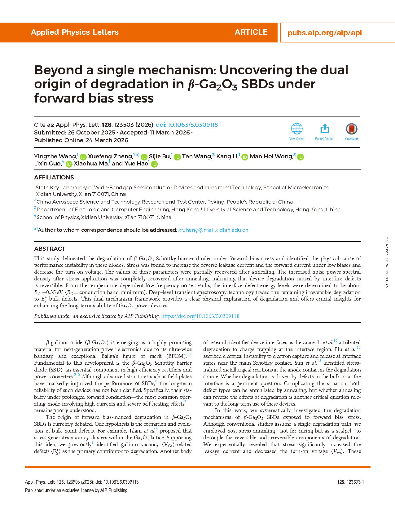
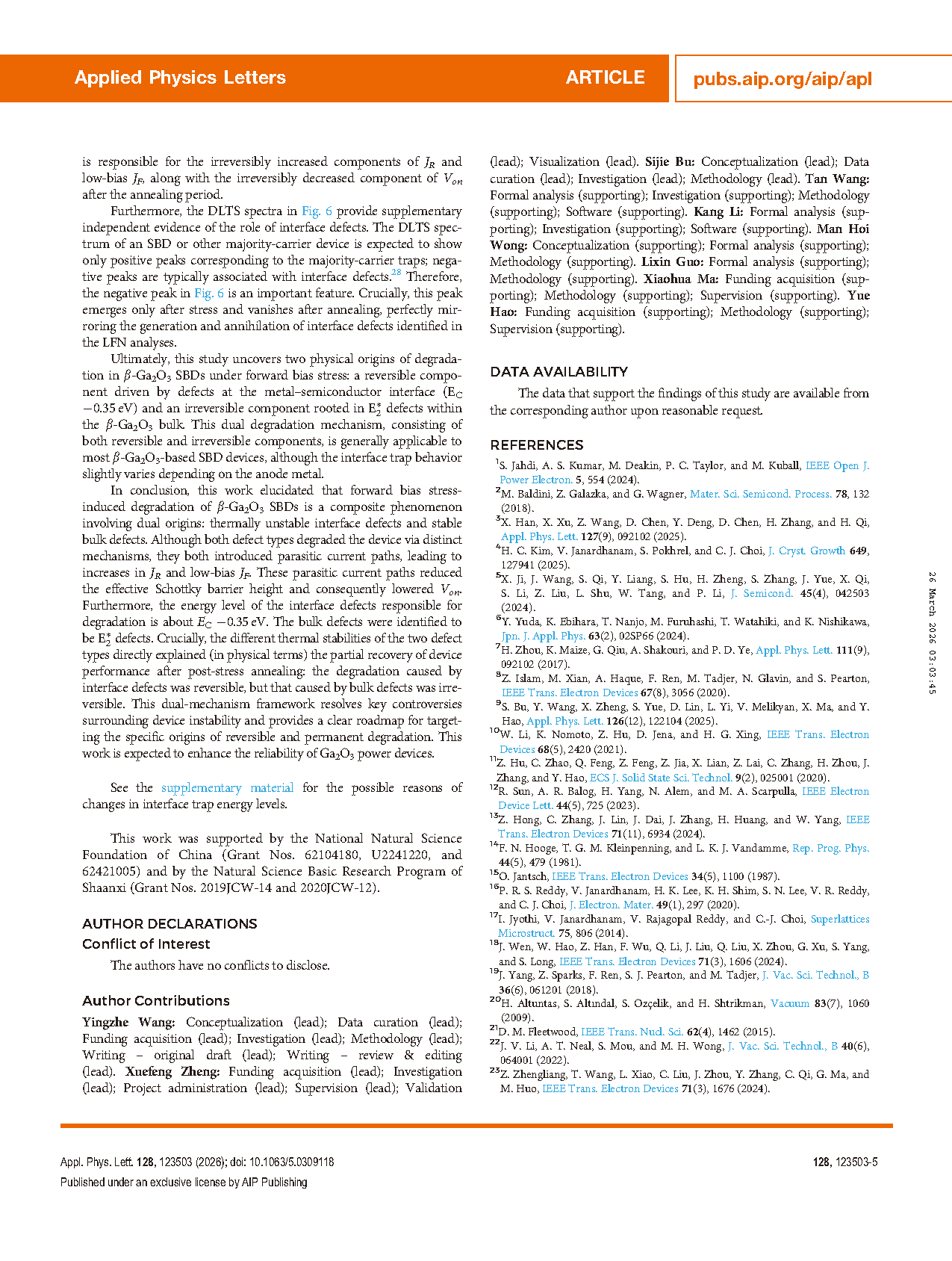
Figure 1. Cross-sectional schematic of β-Ga2O3 SBDs under investigation.
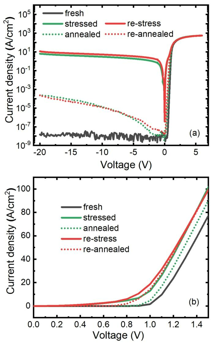
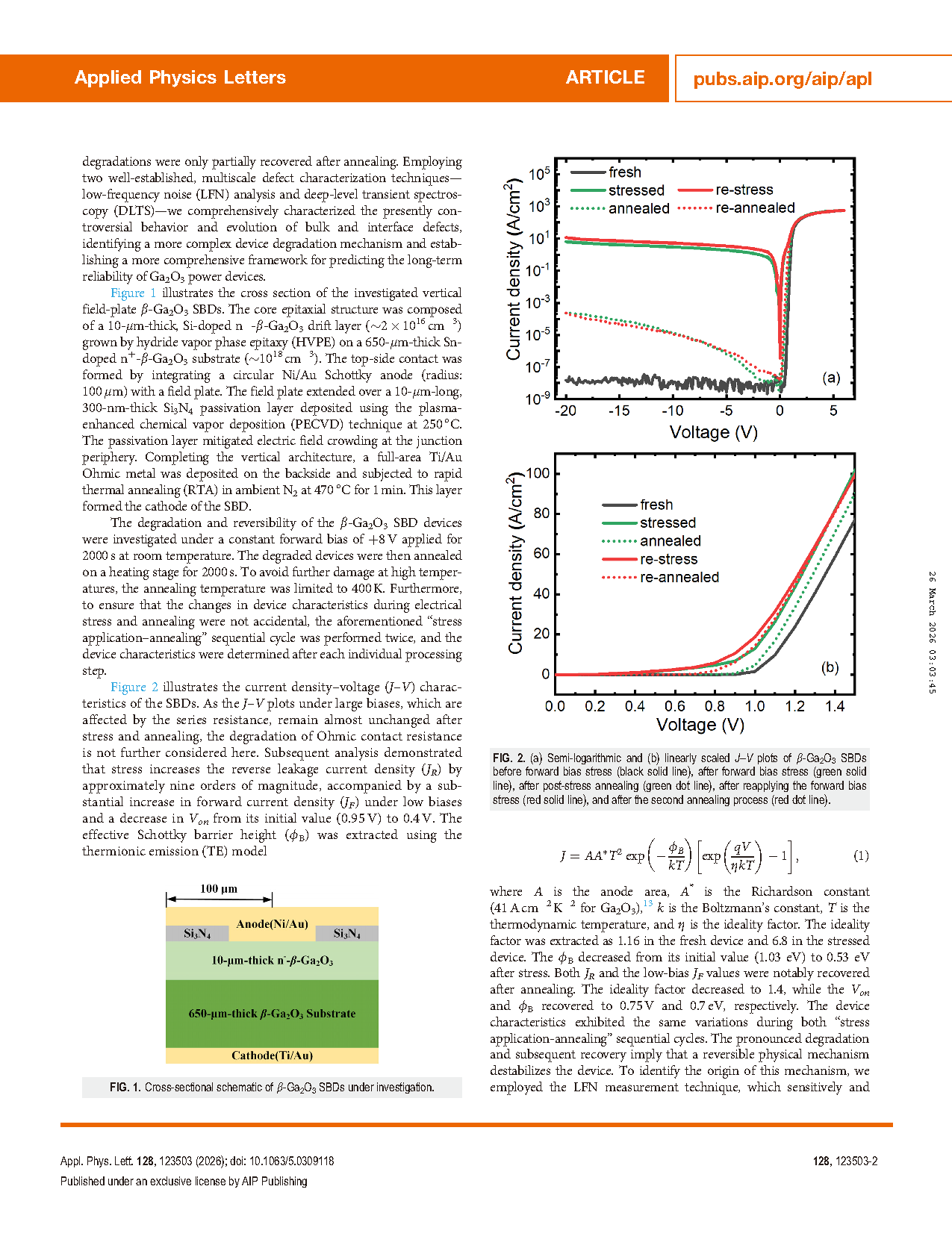
Figure 2. (a) Semi-logarithmic and (b) linearly scaled J–V plots of β-Ga2O3 SBDs before forward bias stress (black solid line), after forward bias stress (green solid line), after post-stress annealing (green dot line), after reapplying the forward bias stress (red solid line), and after the second annealing process (red dot line).
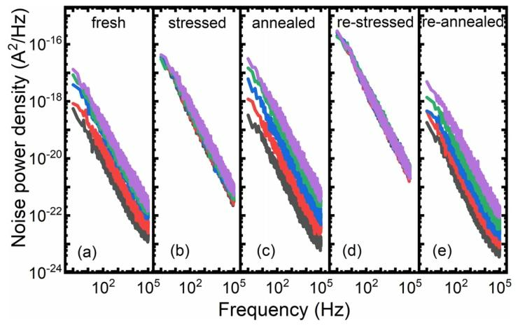
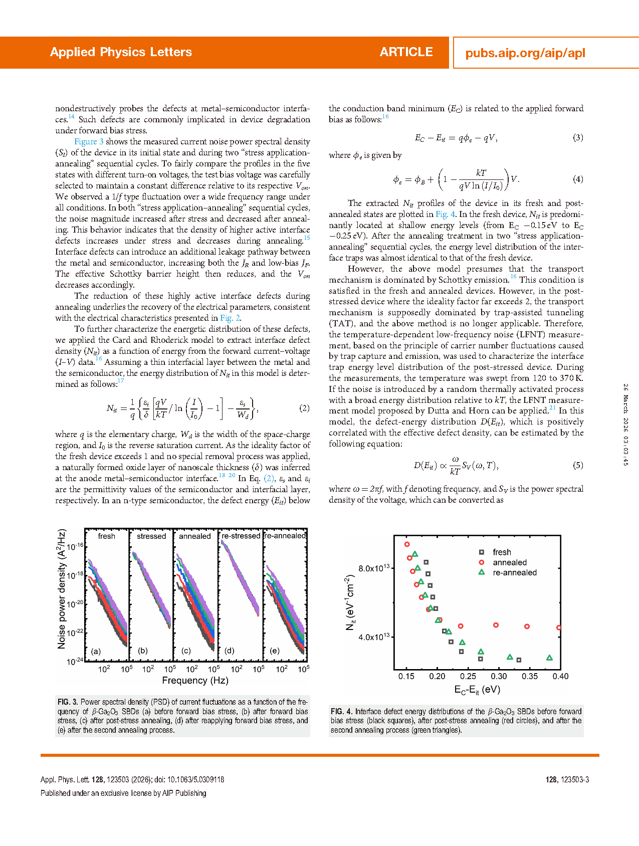
Figure 3. Power spectral density (PSD) of current fluctuations as a function of the frequency of β-Ga2O3 SBDs (a) before forward bias stress, (b) after forward bias stress, (c) after post-stress annealing, (d) after reapplying forward bias stress, and (e) after the second annealing process.
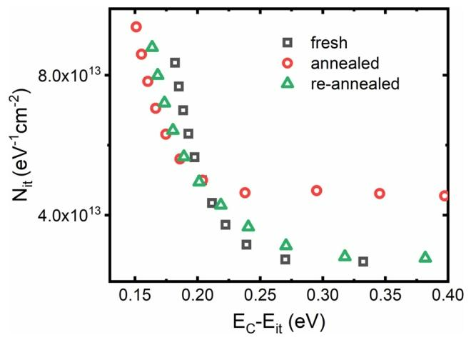
Figure 4. Interface defect energy distributions of the β-Ga2O3 SBDs before forward bias stress (black squares), after post-stress annealing (red circles), and after the second annealing process (green triangles).
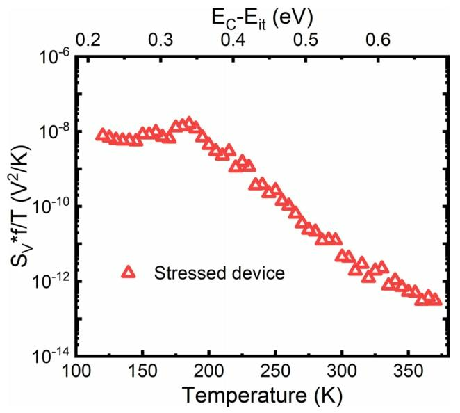
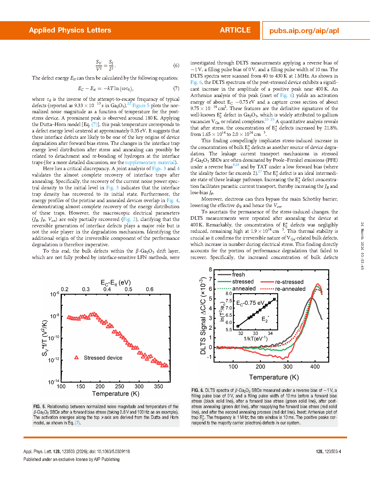
Figure 5. Relationship between normalized noise magnitude and temperature of the β-Ga2O3 SBDs after a forward bias stress (taking 0.8 V and 100 Hz as an example). The activation energies along the top x-axis are derived from the Dutta and Horn model, as shown in Eq. (7).
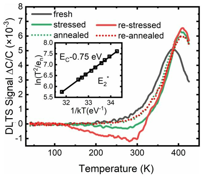
Figure 6. DLTS spectra of β-Ga2O3 SBDs measured under a reverse bias of 1 V, a filling pulse bias of 0 V, and a filling pulse width of 10 ms before a forward bias stress (black solid line), after a forward bias stress (green solid line), after post-stress annealing (green dot line), after reapplying the forward bias stress (red solid line), and after the second annealing process (red dot line). Inset: Arrhenius plot of trap E2*. The frequency is 1 MHz; the rate window is 10 ms. The positive peaks correspond to the majority carrier (electron) defects in our system.
DOI:
doi.org/10.1063/5.0309118