Paper Sharing
【Domestic Papers】Atomic-Scale Insight into Epitaxial Growth and Defect Structures of Metastable α-Ga₂O₃ Thin Films
日期:2026-04-29阅读:197
Researchers from the University of Science and Technology of China, Institute of Metal Research, Chinese Academy of Sciences have published a dissertation titled “Atomic-Scale Insight into Epitaxial Growth and Defect Structures of Metastable α‑Ga₂O₃ Thin Films” in Crystal Growth & Design .
Background
Ultrawide bandgap (UWBG) semiconductors are core materials for next‑generation power electronics and deep‑ultraviolet (DUV) optoelectronics. Metastable corundum‑structured α‑Ga₂O₃ has a wider bandgap (~5.3 eV) and higher symmetry than stable β‑Ga₂O₃, with good lattice matching with Al₂O₃ substrates. However, preparing phase‑pure epitaxial α‑Ga₂O₃ films is difficult due to easy phase transition and defect formation. Pulsed laser deposition (PLD) is suitable for growing metastable phases, but the optimal growth parameters and atomic‑scale defect evolution mechanisms remain unclear.
Abstract
Metastable α‑Ga₂O₃ possesses a wider bandgap and higher symmetry compared to the stable β‑phase, making it a premier candidate for next‑generation power electronics and deep ultraviolet optoelectronics. However, achieving pure‑phase epitaxy and understanding the nanoscale defect evolution remain significant challenges. Here, we report the high‑crystallinity growth of pure α‑Ga₂O₃ thin films on (11-20) Al₂O₃ substrates via pulsed laser deposition. By systematically tailoring the growth temperature (600−800 °C) and O₂ partial pressure (0.01−10 Pa), we identified 750 °C and 5 Pa as the optimal parameters for growing α‑Ga₂O₃ thin films. Aberration‑corrected scanning transmission electron microscopy reveals that an atomically flat and coherent interface is formed between α‑Ga₂O₃ and Al₂O₃ characterized by direct Ga−O bonding without elemental diffusion. A high‑density network of stacking faults (SFs) was formed in the α‑Ga₂O₃ thin film. It revealed that the basal‑plane SFs have sharp interfaces, and the faults are caused by the relative sliding between Ga and O atomic layers along the (0001) plane. Our findings provide critical atomic‑scale insights into the structural engineering of corundum‑structured oxides for advanced semiconductor applications.
Highlights
Determined the optimal PLD growth parameters (750 °C, 5 Pa) for phase‑pure and high‑crystallinity α‑Ga₂O₃ thin films on Al₂O₃ (11-20) substrates.
Directly observed the atomically flat, coherent α‑Ga₂O₃/Al₂O₃ interface with Ga−O direct bonding and no elemental diffusion at the atomic scale.
Clarified the atomic structure and formation mechanism of high‑density basal‑plane stacking faults in α‑Ga₂O₃.
Conclusion
In summary, we have demonstrated the high‑crystallinity epitaxial growth of metastable α‑Ga₂O₃ thin films on Al₂O₃ substrates by precisely optimizing PLD parameters. Our research results identified the optimal parameters for obtaining phase‑pure α‑Ga₂O₃ thin films with excellent crystallinity as 750 °C and 5 Pa. Atomic‑scale investigations via aberration‑corrected STEM reveal an atomically flat and coherent α‑Ga₂O₃/Al₂O₃ interface with direct Ga−O bonding. Furthermore, we identified the presence of high‑density basal‑plane SFs, which facilitate strain relaxation in the epitaxial film. These findings provide a comprehensive understanding of the growth kinetics and defect chemistry of α‑Ga₂O₃, laying a critical foundation for the development of high‑performance deep‑ultraviolet optoelectronic devices based on corundum‑structured oxides.
Project Support
This study was supported by the Jihua Laboratory (No. X210141TL210).
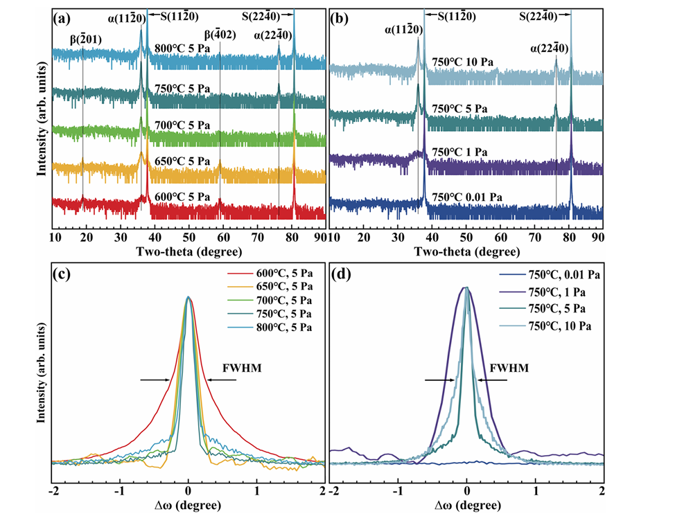
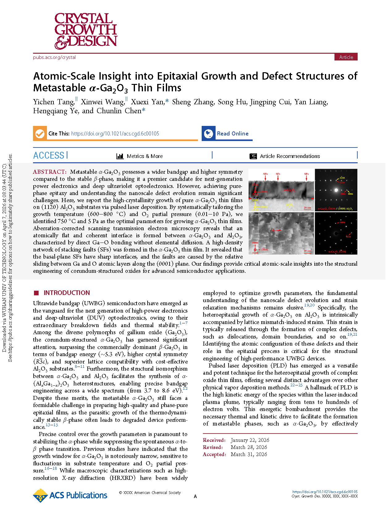
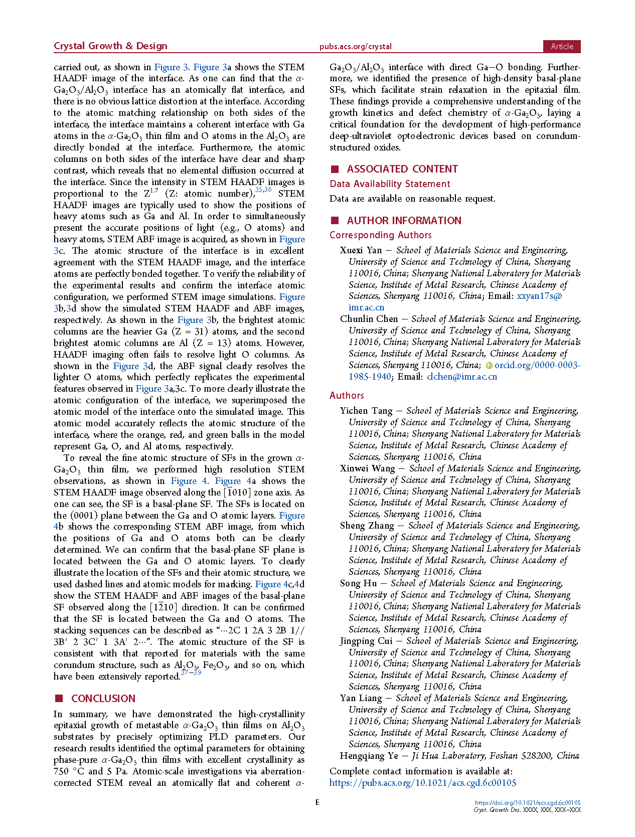
Figure 1 HRXRD patterns of -Ga₂O₃ thin films grown on Al₂O₃ (11-20) substrates. (a) HRXRD patterns of films grown at a fixed O₂ partial pressure of 5 Pa with temperatures ranging from 600 to 800 °C. The evolution from a mixed and -phase (600–650 °C) to a pure metastable -phase (700–800 °C) is observed. (b) HRXRD patterns of films grown at 750 °C under different O₂ partial pressures from 0.01–10 Pa. (c, d) Rocking curves of the (11-20) peak of -Ga₂O₃ thin films grown at different temperatures and O₂ pressures. The FWHMs of -Ga₂O₃ films grown at 600–800 °C are 0.44°, 0.36°, 0.28°, 0.18°, and 0.22°, respectively. And the FWHMs of -Ga₂O₃ films grown at 1–10 Pa are 0.62°, 0.22°, and 0.35°, respectively. The optimal growth parameters of -Ga₂O₃ thin films are 750 °C and 5 Pa.
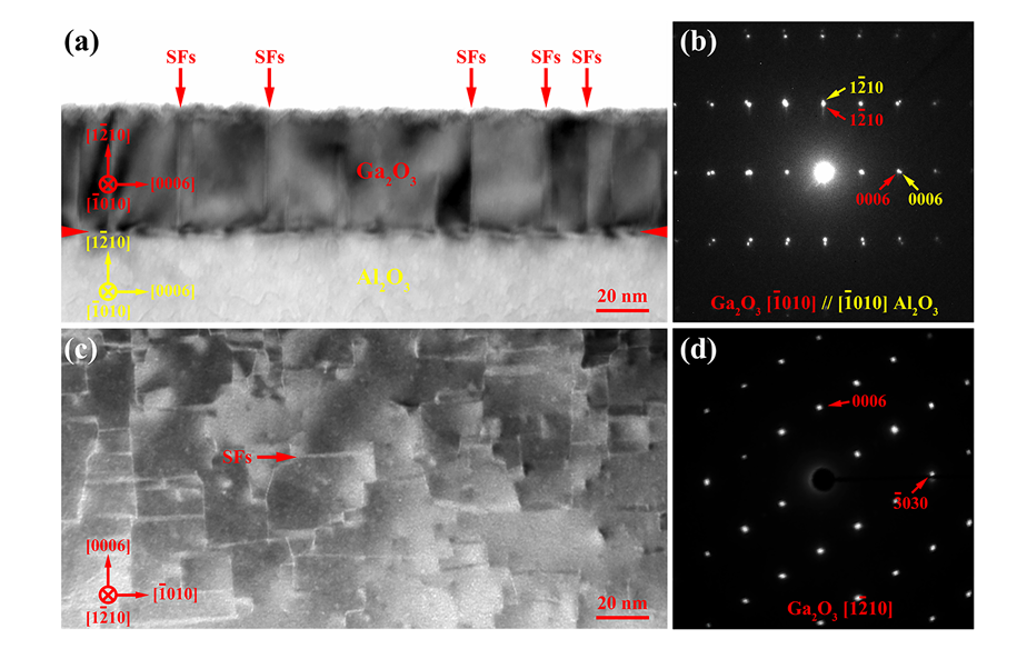
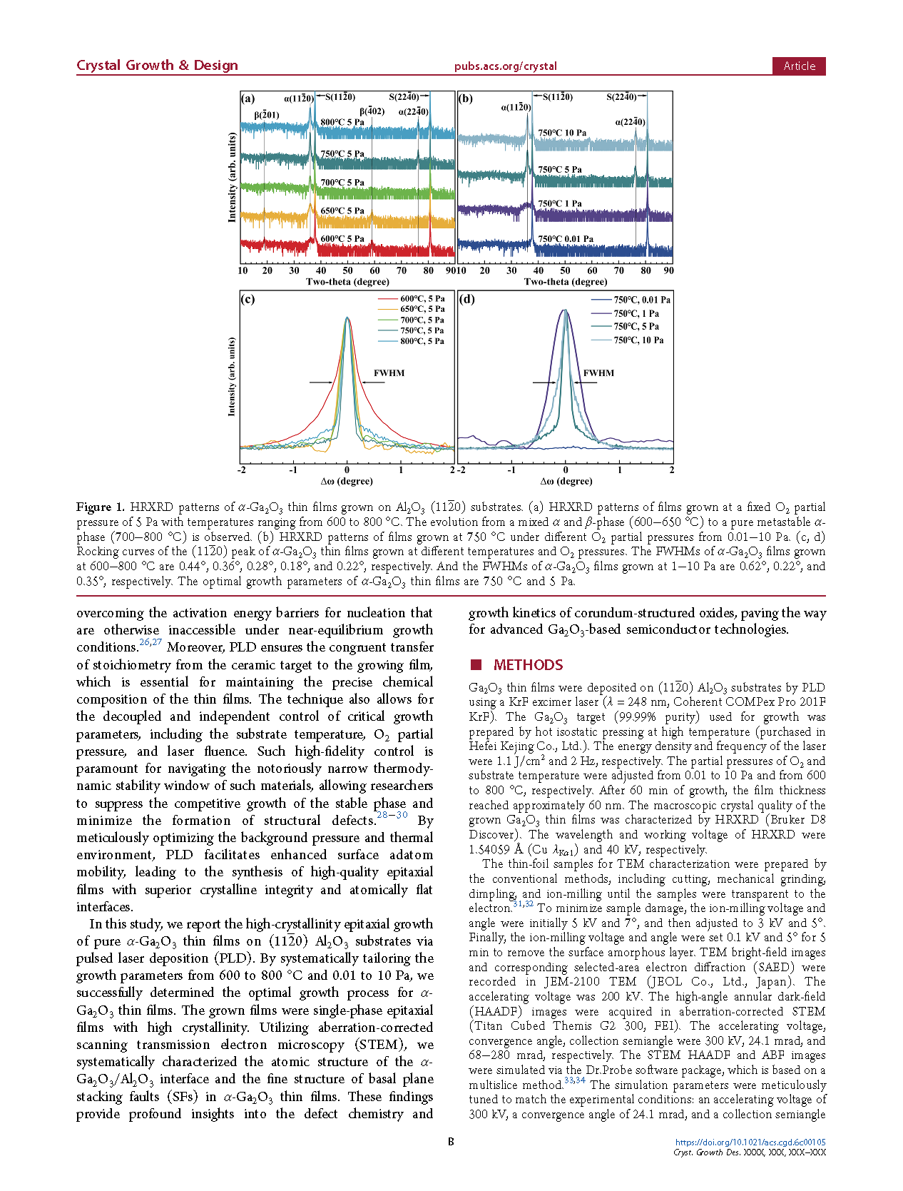
Figure 2 Microstructure of the α-Ga₂O₃/Al₂O₃ thin film. (a) TEM bright-field image observed along the [100] zone axis, showing a uniform film thickness of 60 nm and high-density SFs perpendicular to the substrate. (b) Corresponding SAED pattern at the interface confirming the epitaxial relationship: α-Ga₂O₃ (1-210) [10-10] // Al₂O₃ (1-210) [10-10]. (c) TEM bright-field image along the [-12-10] zone axis revealing a high-density network of basal-plane and prismatic SFs. (d) Corresponding SAED pattern. The grown α-Ga₂O₃ thin film is a single crystal film.
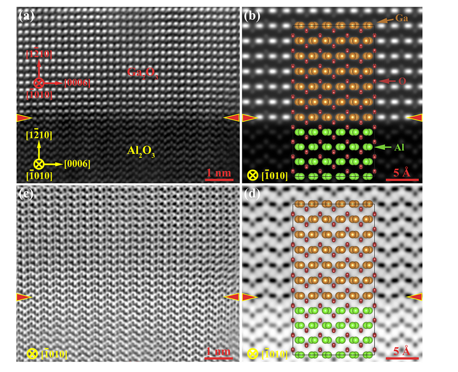
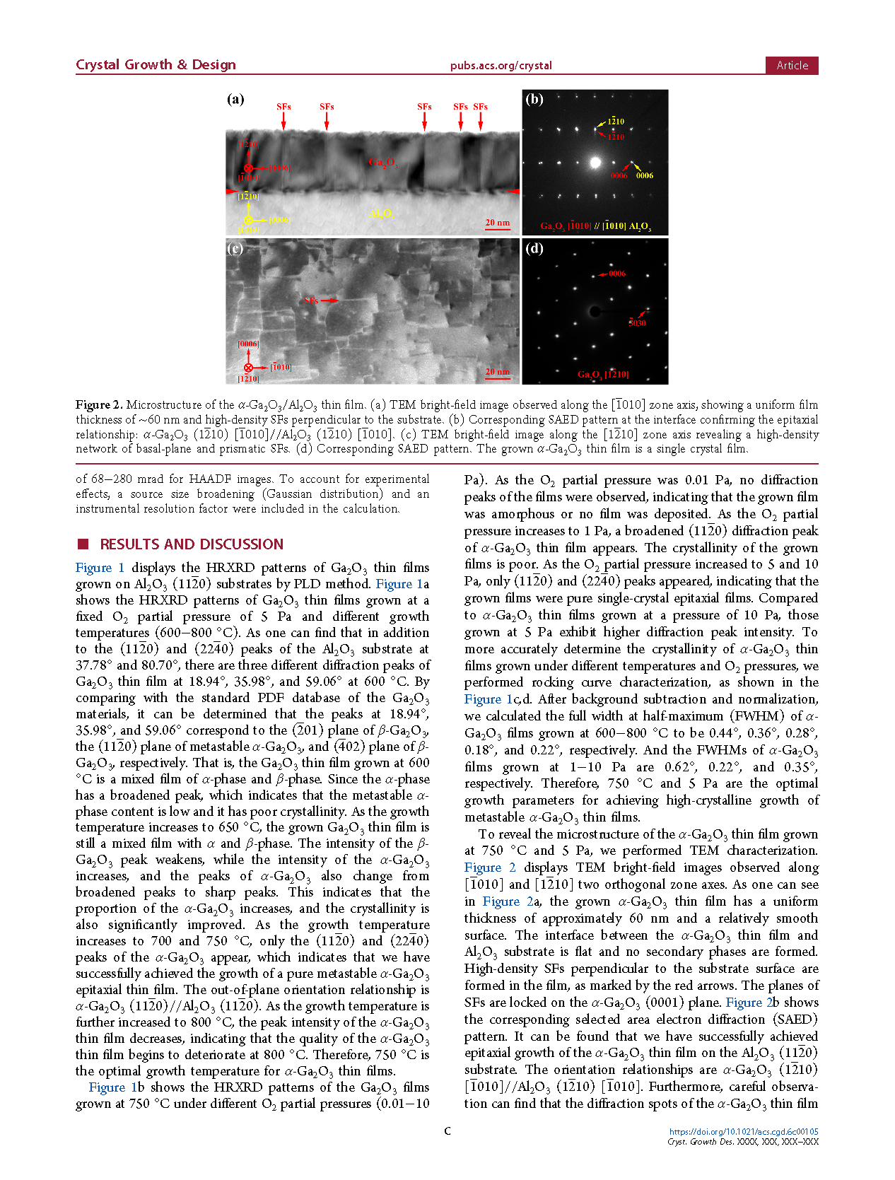
Figure 3 Atomic structures of the α-Ga₂O₃/Al₂O₃ interfaces. (a) Aberration-corrected STEM HAADF image projected along [010] zone axis. The α-Ga₂O₃/Al₂O₃ interface displays an atomically flat and coherent interface without obvious lattice distortion. (b) Corresponding simulated STEM HAADF image superimposed with the atomic model, which is in agreement with experimental image. The orange, red, and green balls represent the Ga, O, and Al atoms, respectively. (c) STEM ABF image simultaneously observed with HAADF image (a). (d) Corresponding simulated STEM ABF image.
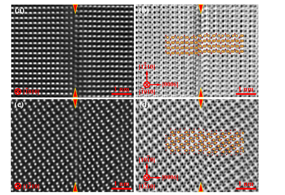
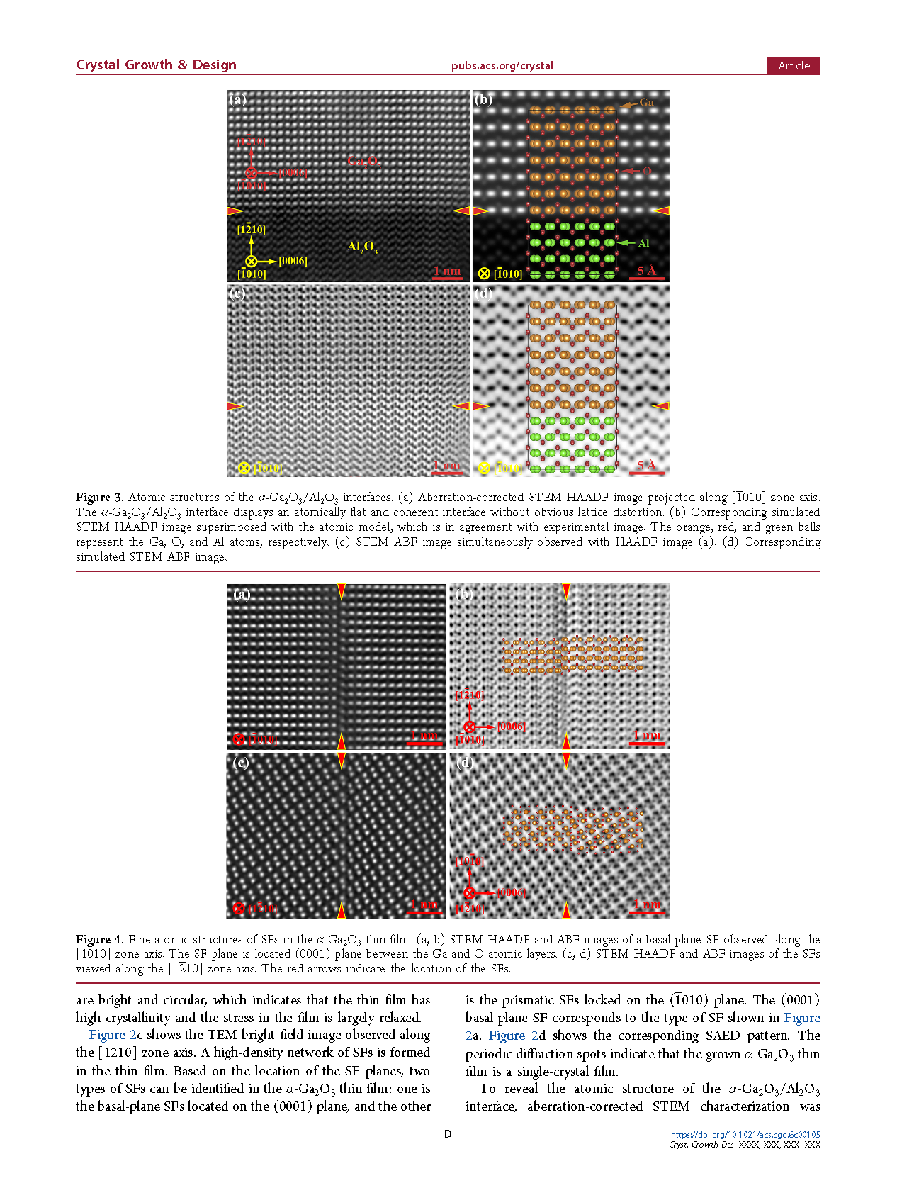
Figure 4 Fine atomic structures of SFs in the α-Ga₂O₃ thin film. (a, b) STEM HAADF and ABF images of a basal-plane SF observed along the [10-10] zone axis. The SF plane is located (0001) plane between the Ga and O atomic layers. (c, d) STEM HAADF and ABF images of the SFs viewed along the [-12-10] zone axis. The red arrows indicate the location of the SFs.
DOI:
doi.org/10.1021/acs.cgd.6c00105