Paper Sharing
【Member Papers】 Valence band elevation and acceptor behavior in sulfur-alloyed Ga₂O₃
日期:2026-04-30阅读:235
Researchers from the Institute of Semiconductors, Chinese Academy of Sciences, Shenzhen University and National University of Defense Technology have published a dissertation titled "Valence band elevation and acceptor behavior in sulfur-alloyed Ga₂O₃" in Physical Review B.
Background
Wide-band-gap semiconductors have broad application prospects in electronic and optoelectronic fields such as harsh-environment sensors, high-power transistors and solar-blind photodetectors due to their excellent properties like high breakdown field strength and strong radiation resistance. Among them, α‑Ga₂O₃ is highly attractive in high-power electronic devices for its largest band gap. However, similar to common wide-band-gap metal oxides such as ZnO and SnO₂, Ga₂O₃ faces a major challenge in achieving efficient p-type doping because its valence-band maximum is low-lying and strongly localized, dominated by O 2p orbitals. Although cation alloying has been proven to regulate the electronic structure of Ga₂O₃, and chalcogen anion alloying is expected to raise the valence-band maximum to facilitate p-type doping, the detailed acceptor behavior in α‑Ga₂(SₓO₁₋ₓ)₃ alloys, especially which acceptor impurities are more favorable in the alloys, is still unclear.
Abstract
Efficient P-type doping in wide-band-gap (WBG) oxides is fundamentally hindered by their low-lying and localized valence-band maximum (VBM). One promising approach to overcome this limitation is to elevate the VBM through alloy formation. Although the tuning of electronic structures in semiconductor alloys has been widely explored, the defect behavior in such systems remains poorly understood. Here, using first-principles calculations, we investigate the electronic structure and acceptor behavior of dilute α‑Ga₂(SₓO₁₋ₓ)₃ anion alloys. We show that S incorporation significantly raises the VBM of Ga₂O₃, thereby creating favorable conditions for P-type doping. Among eight candidate acceptors, BeGa, MgGa, CaGa, SrGa, ZnGa, and CdGa remain deep acceptors in the alloy, whereas the very deep AgGa and, notably, CuGa levels in α‑Ga₂O₃ become much shallower upon alloying. Charge-density analysis reveals that the former six defects form hole-polaron states strongly coupled to the VBM, while AgGa and CuGa are decoupled from the VBM.
Highlights
Using first-principles calculations to investigate the electronic structure and acceptor behavior of dilute α‑Ga₂(SₓO₁₋ₓ)₃ anion alloys.
S incorporation significantly raises the VBM of Ga₂O₃, creating favorable conditions for P-type doping.
BeGa, MgGa, CaGa, SrGa, ZnGa and CdGa remain deep acceptors in the alloy, while AgGa and CuGa become much shallower.
The former six defects form hole-polaron states strongly coupled to the VBM, while AgGa and CuGa are decoupled from the VBM.
Conclusion
In summary, we have systematically investigated the electronic structure and acceptor behavior of dilute Ga₂(SₓO₁₋ₓ)₃ alloys using first-principles calculations. Our results show that S alloying significantly elevates the VBM of Ga₂O₃, creating favorable conditions for p-type doping. Calculations of eight candidate acceptors reveal that BeGa, MgGa, CaGa, SrGa, ZnGa and CdGa remain deep acceptors in the dilute alloy, whereas the very deep AgGa and especially CuGa levels in α‑Ga₂O₃ become much shallower in the dilute alloy, making Cu a promising p-type dopant. Analysis of hole charge densities indicates that the hole states of the former six acceptors strongly couple to the VBM and form hole-polaron states, while AgGa and CuGa defect states are decoupled from the VBM. Our study provides insights into p-type doping in Ga₂O₃ and related WBG alloys.
Project Support
This paper was supported by the National Natural Science Foundation of China (Grants No. 62425406, No. 12474073, No. 12504286, and No. 12504290), the National Key Research and Development Program of China (Grant No. 2024YFA1409700), the Strategic Priority Research Program of the Chinese Academy of Sciences (Grant No. XDB0460000), the CAS Project for Young Scientists in Basic Research (No. YSBR-026), the Guangdong Basic and Applied Basic Research Foundation (Grant No. 2025A1515011292), and the Innovation Research Foundation of National University of Defense Technology.
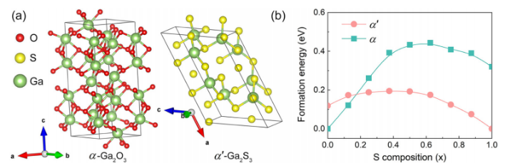
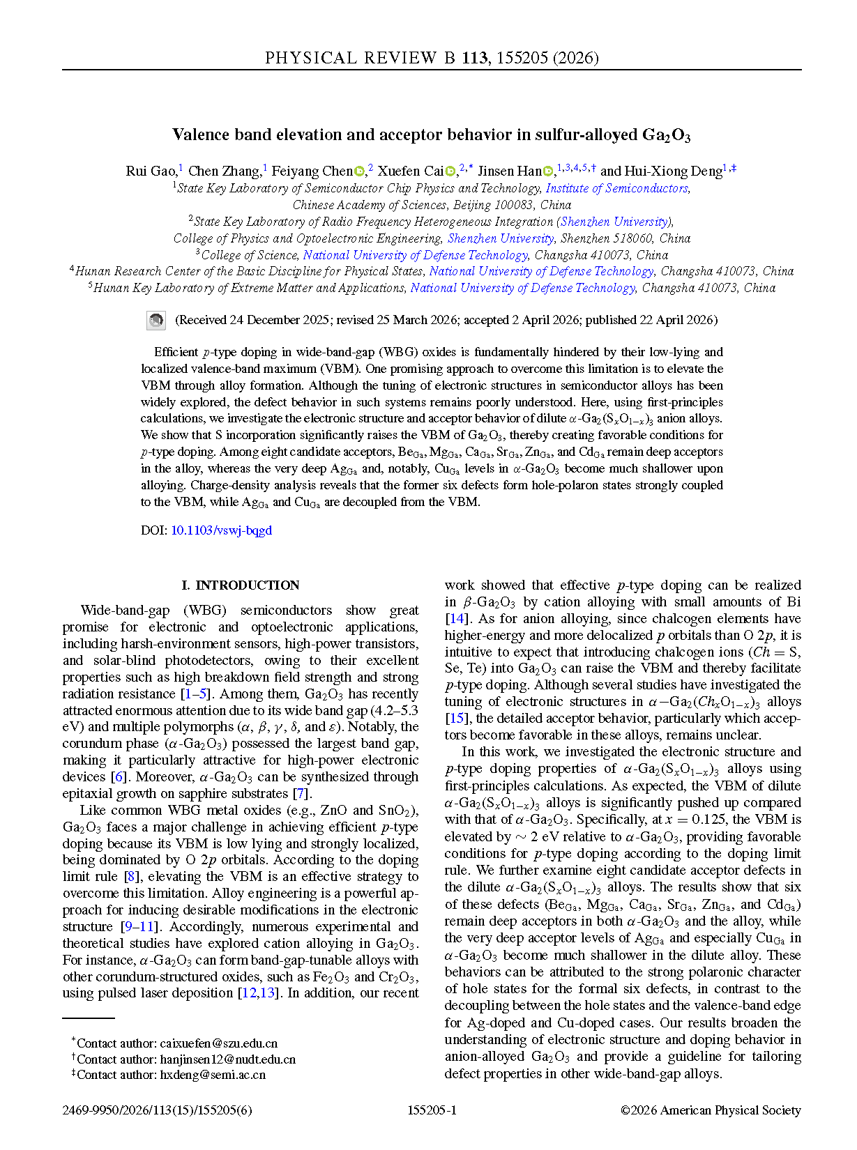
FIG. 1. (a) The conventional unit cell of corundum Ga₂O₃ and monoclinic Ga₂S₃, where red, yellow, and green spheres represent O, S, and Ga atoms, respectively. (b) The formation energies of Ga₂(SₓO₁₋ₓ)₃ alloy as functions of S composition with green squares denoting corundum structure (α) and red circles representing monoclinic structure (α′).
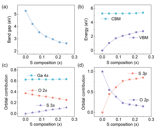
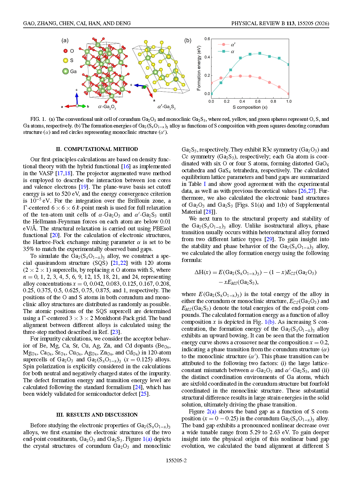
FIG. 2. (a) Band gaps, (b) band edge positions, and corresponding atomic orbital contributions for CBM (c) and VBM (d) of Ga₂(SₓO₁₋ₓ)₃ alloy as functions of S concentrations x.
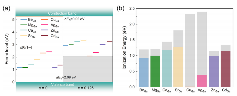
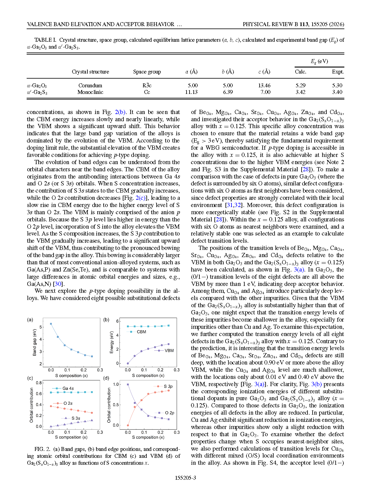
FIG. 3. (a) Thermodynamic transition levels (0/1−) for different substitutional dopants in Ga₂O₃ and Ga₂(SₓO₁₋ₓ)₃ alloy (x = 0.125), referenced to their respective VBMs. The valence band offsets (VBOs) and conduction band offsets (CBOs) between the two systems are also indicated. (b) Corresponding ionization energies of different substitutional dopants in pure Ga₂O₃ and Ga₂(SₓO₁₋ₓ)₃ alloy (x = 0.125). Colored bars represent ionization energies of different dopants in the alloys, while gray bars indicate the corresponding values in Ga₂O₃.
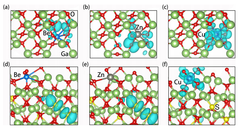
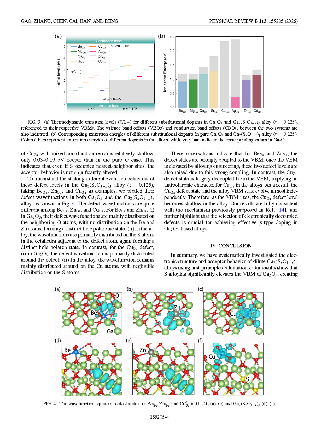
FIG. 4. The wavefunction square of defect states for Be⁰Ga, Zn⁰Ga, and Cu⁰Ga in Ga₂O₃ (a)–(c) and Ga₂(SₓO₁₋ₓ)₃ (d)–(f).
DOI:
doi.org/10.1103/vswj-bqgd