Paper Sharing
【Member Papers】 Geometric and Thermal Control of κ- to β-Ga₂O₃ Phase Engineering for High-Performance Solar-Blind Photodetector
日期:2026-04-30阅读:224
Researchers from Northeast Normal University and City College of New York have published a dissertation titled “Geometric and Thermal Control of κ‑ to β‑Ga₂O₃ Phase Engineering for High-Performance Solar-Blind Photodetector” in Materials Today Physics.
Background
Solar-blind ultraviolet photodetectors are of great significance in environmental monitoring and deep-space imaging. Ultra-wide bandgap Ga₂O₃ is an ideal candidate due to its excellent photoelectric properties. Thermodynamically stable β‑Ga₂O₃ has low lattice symmetry, which easily leads to lattice mismatch and high-density defects during heteroepitaxy, making it difficult to obtain high-quality films. Homoepitaxy can alleviate defect issues, but the fabrication of single-crystal substrates is difficult and costly, limiting the performance improvement and large-scale application of devices. At present, research on preparing high-quality β‑Ga₂O₃ films via controllable phase transformation using metastable κ‑Ga₂O₃ as a precursor is still insufficient, and the regulation rules of growth temperature and annealing process on phase transformation are not clear.
Abstract
By varying the growth temperature in metalorganic chemical vapor deposition (MOCVD), we achieved controlled growth of (002)-oriented κ‑Ga₂O₃, a κ‑β mixed phase, and (-201)-oriented β‑Ga₂O₃ on c-plane sapphire. The highly aligned orientation of κ‑Ga₂O₃ grains is attributed to a superior lattice symmetry match with the c-plane sapphire substrate, as evidenced by a narrow ω-scan rocking curve (FWHM < 0.6°). To achieve β‑Ga₂O₃ films with superior crystallinity, a postgrowth annealing strategy was employed to transform the metastable κ-phase into the thermodynamically stable β-phase. At an optimized annealing temperature of 1000 ℃, the resulting β‑Ga₂O₃ film exhibits significant improvements in both crystal quality and surface morphology. The FWHM of the (-201) rocking curve was drastically reduced from the as grown 2.25° to 0.77°, and the surface roughness is reduced from 11.3 nm to 4.17 nm. At 10 V bias, the β‑Ga₂O₃ based solar-blind ultraviolet (UV) photodetector achieves a responsivity of 98 A/W, a detectivity of 1.3 × 10¹⁷ Jones and a high UV/visible rejection ratio (Rₘₐₓ / R₄₀₀) exceeding 10⁶. This work establishes a reliable approach for controllable preparation of Ga₂O₃ films with different phases and for the fabrication of high-quality β‑Ga₂O₃ films suitable for optoelectronic device applications.
Highlights
Realized controllable growth of κ‑phase, κ‑β mixed-phase and β‑phase Ga₂O₃ films on c-plane sapphire by tuning MOCVD growth temperature.
Obtained high-quality κ‑Ga₂O₃ films with narrow rocking curve FWHM below 0.6° on c-plane sapphire substrates.
Transformed metastable κ‑Ga₂O₃ into high-crystallinity β‑Ga₂O₃ via postannealing at 1000 ℃, significantly improving crystal quality and surface morphology.
Fabricated high-performance solar-blind UV photodetectors with ultrahigh detectivity of 1.3 × 10¹⁷ Jones and UV/visible rejection ratio over 10⁶.
Demonstrated a feasible phase engineering strategy for optimizing the performance of Ga₂O₃-based optoelectronic devices.
Conclusion
This study achieved controlled phase transformation in Ga₂O₃ films, from κ-phase through κ‑β mixed phase, to β-phase, by precisely regulating the growth and annealing temperatures. The pre-grown high-quality κ‑Ga₂O₃ serves as a precursor phase, guiding its atomic reconstruction into β‑Ga₂O₃ during subsequent annealing. The resulting film, with its narrower XRD rocking curve (FWHM = 0.77°) and lower surface roughness (RMS = 4.17 nm), demonstrates crystalline quality far superior to that achieved by direct growth. Consequently, the fabricated UV photodetector demonstrates outstanding performance, with a high responsivity of 98 A/W and a large rejection ratio (Rₘₐₓ / R₄₀₀) exceeding 10⁶. This work paves the way for developing high-quality Ga₂O₃-based solar-blind UV photodetectors.
Project Support
This work was supported by the National Natural Science Foundation of China (NO. 62274027 and 62404039), the Open Research Fund of Song Shan Lake Materials Laboratory (2023SLABFK03), 111 Center (B25030) and the Funding from Jilin Province (NO. 20220502002GH), the Scientific Research Project of Education Department of Jilin Province (JJKH20250304BS).
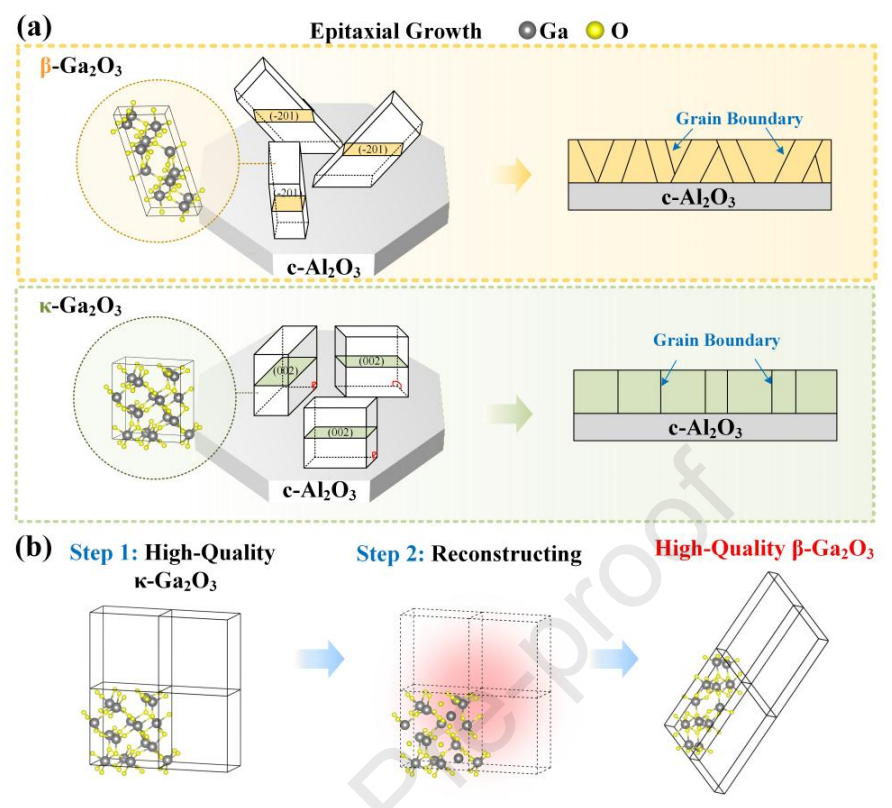
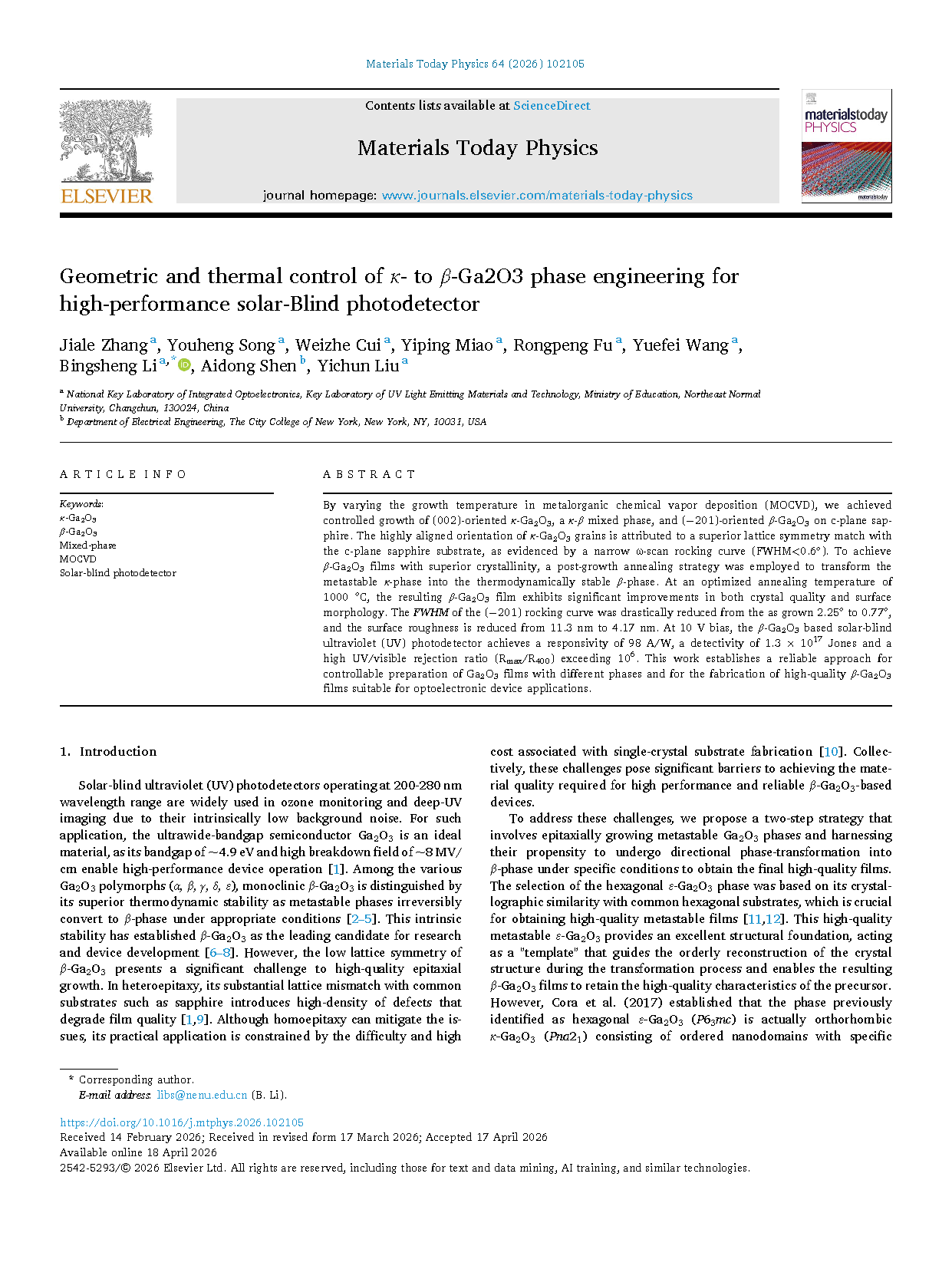
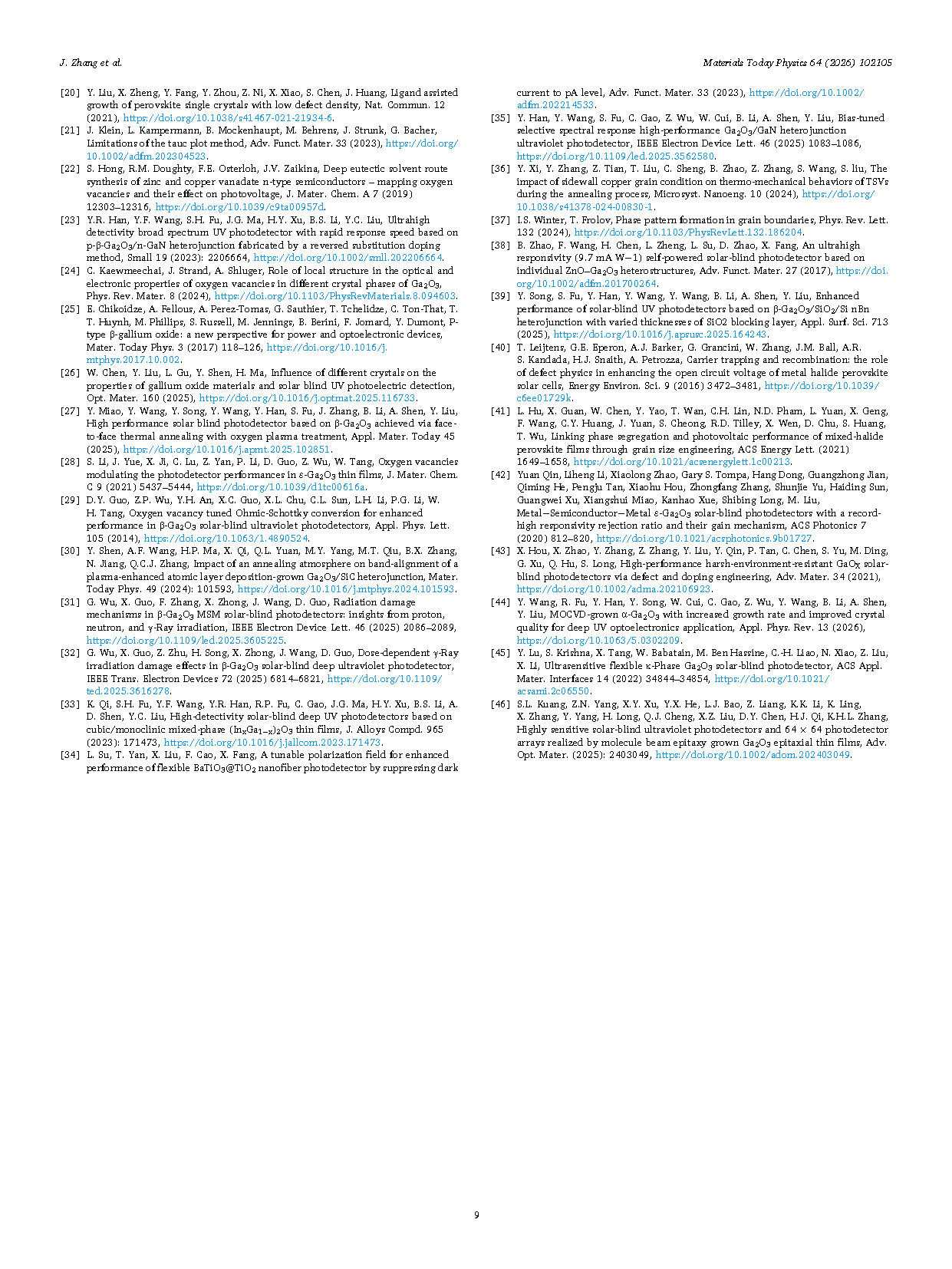
Figure 1. (a) Schematic diagrams of the epitaxial growth of β‑Ga₂O₃ and κ‑Ga₂O₃ films on c-plane sapphire substrates. (b) Schematic diagrams illustrating the epitaxial growth and subsequent phase transformation approach used to obtain high-quality β‑Ga₂O₃ films.
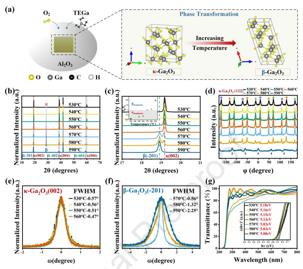
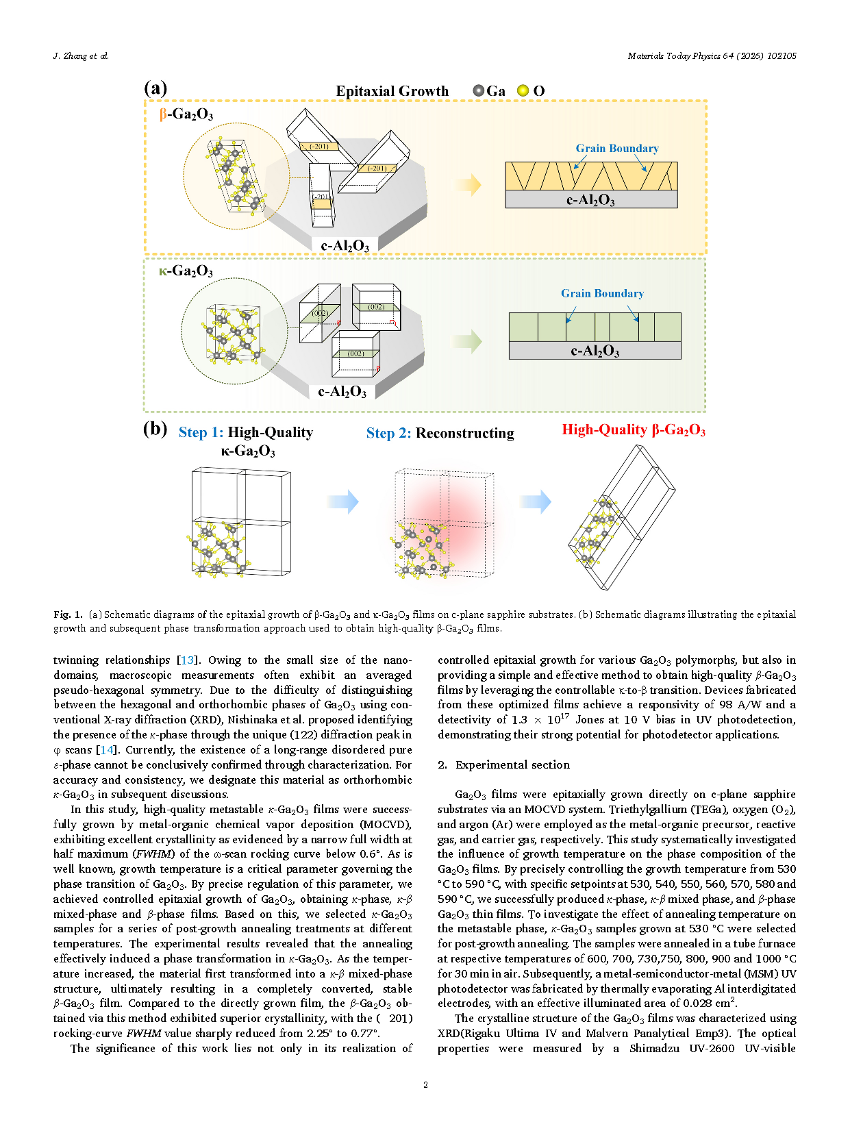
Figure 2. Structural and optical characterization of Ga₂O₃ films grown at different temperatures. (a) Schematic illustration of the epitaxial growth and phase transition of Ga₂O₃ on a c-plane sapphire substrate. (b) XRD patterns. (c) Locally magnified XRD patterns; the inset displays intensity ratio (Iᵦ / Iκ) between the β‑Ga₂O₃ (-201) and κ‑Ga₂O₃ (002) diffraction peaks for each temperature. (d) φ-scan of the κ‑Ga₂O₃ (122) plane. XRD rocking curve of (e) the (002) plane for κ‑Ga₂O₃ and (f) the (-201) plane for β‑Ga₂O₃. (g) Transmission spectrum with the corresponding Tauc plot in the inset.
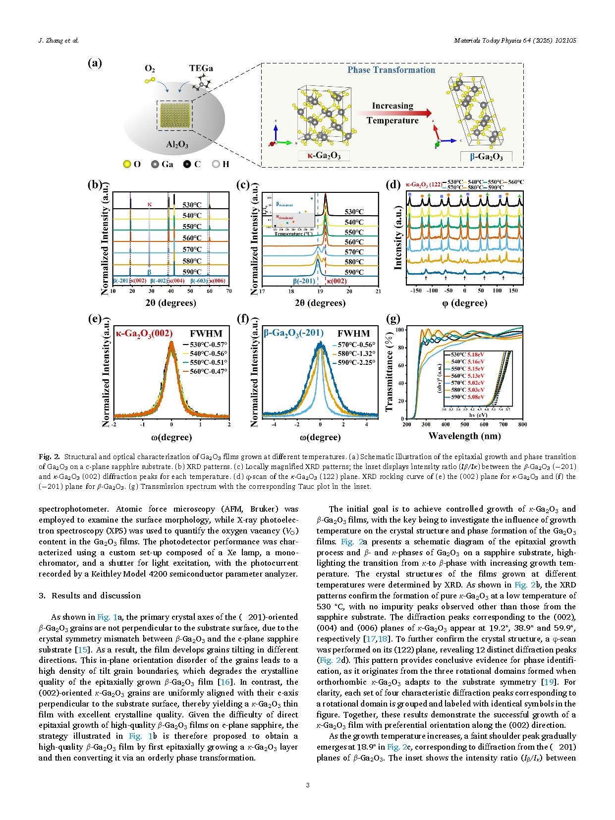
Figure 3. Electronic band structure of (a) κ‑Ga₂O₃ and (b) β‑Ga₂O₃, calculated using density functional theory, showing theoretical bandgap values of 5.24 eV and 4.90 eV for κ‑Ga₂O₃ and β‑Ga₂O₃, respectively.
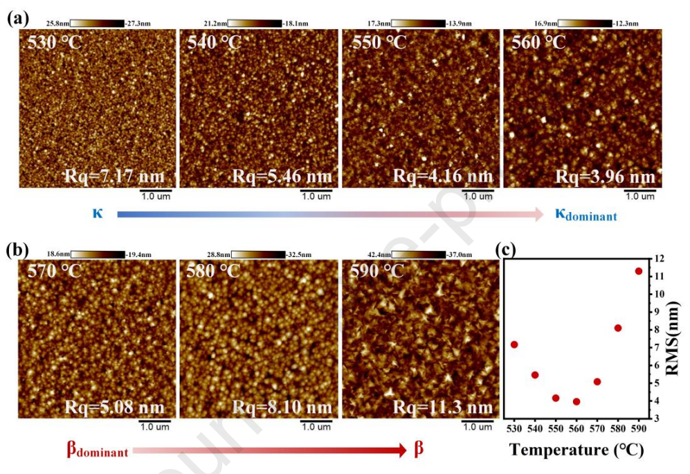
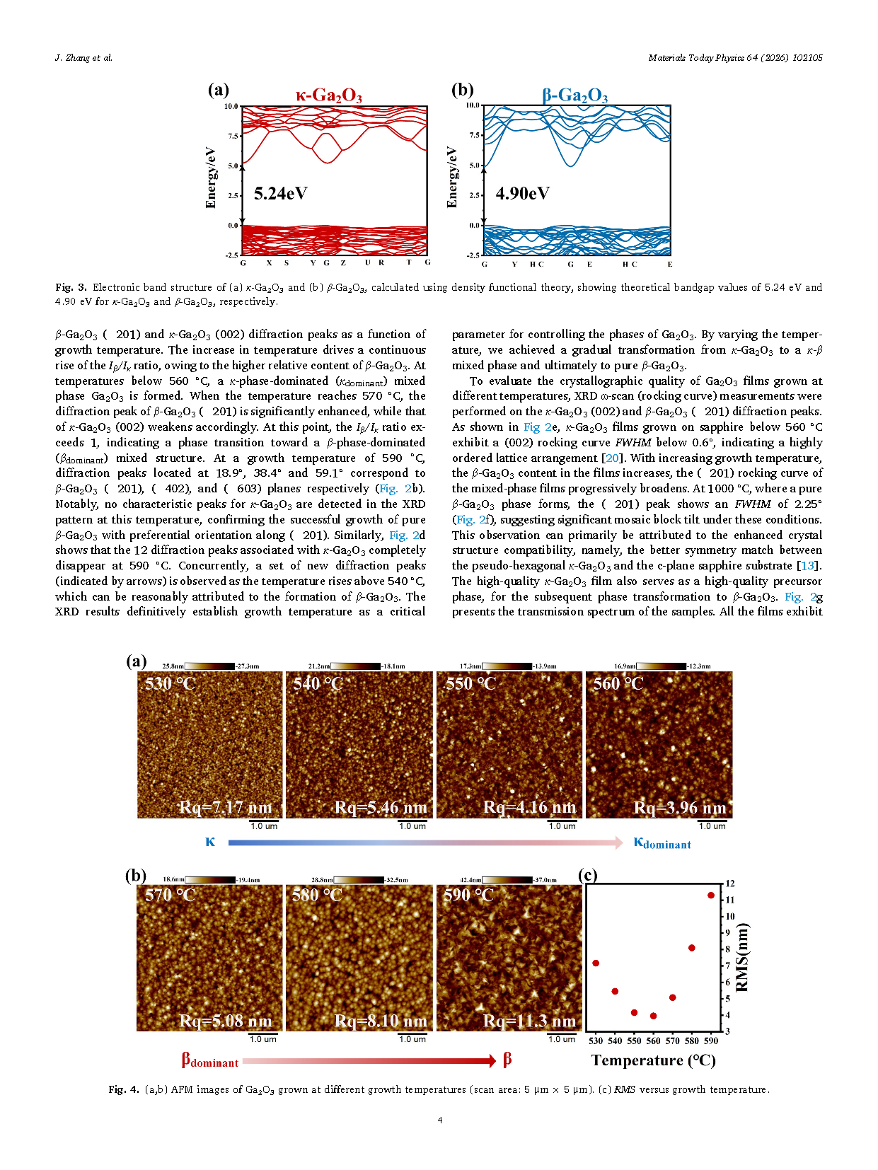
Figure 4. (a,b) AFM images of Ga₂O₃ grown at different growth temperatures (scan area: 5 μm × 5 μm). (c) RMS versus growth temperature.
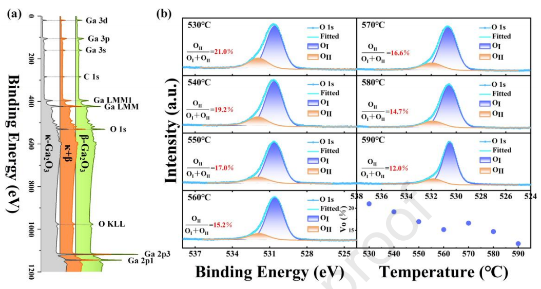
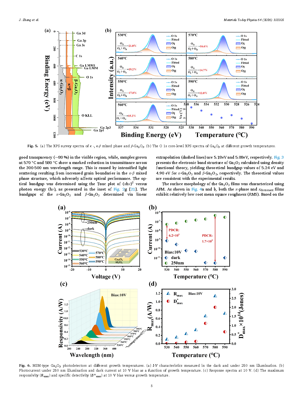
Figure 5. (a) The XPS survey spectra of κ‑, κ‑β mixed phase and β‑Ga₂O₃. (b) The O 1s core-level XPS spectra of Ga₂O₃ at different growth temperatures.
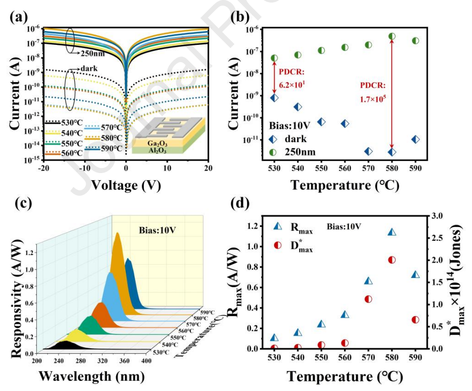
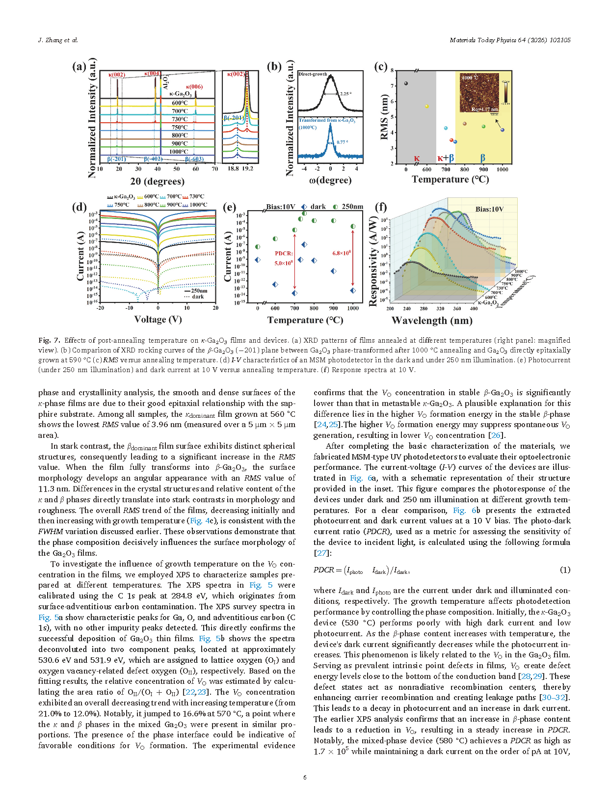
Figure 6. MSM-type Ga₂O₃ photodetectors at different growth temperatures. (a) I–V characteristics measured in the dark and under 250 nm illumination. (b) Photocurrent under 250 nm illumination and dark current at 10 V bias as a function of growth temperature. (c) Response spectra at 10 V. (d) The maximum responsivity (Rₘₐₓ) and specific detectivity (D*ₘₐₓ) at 10 V bias versus growth temperature.
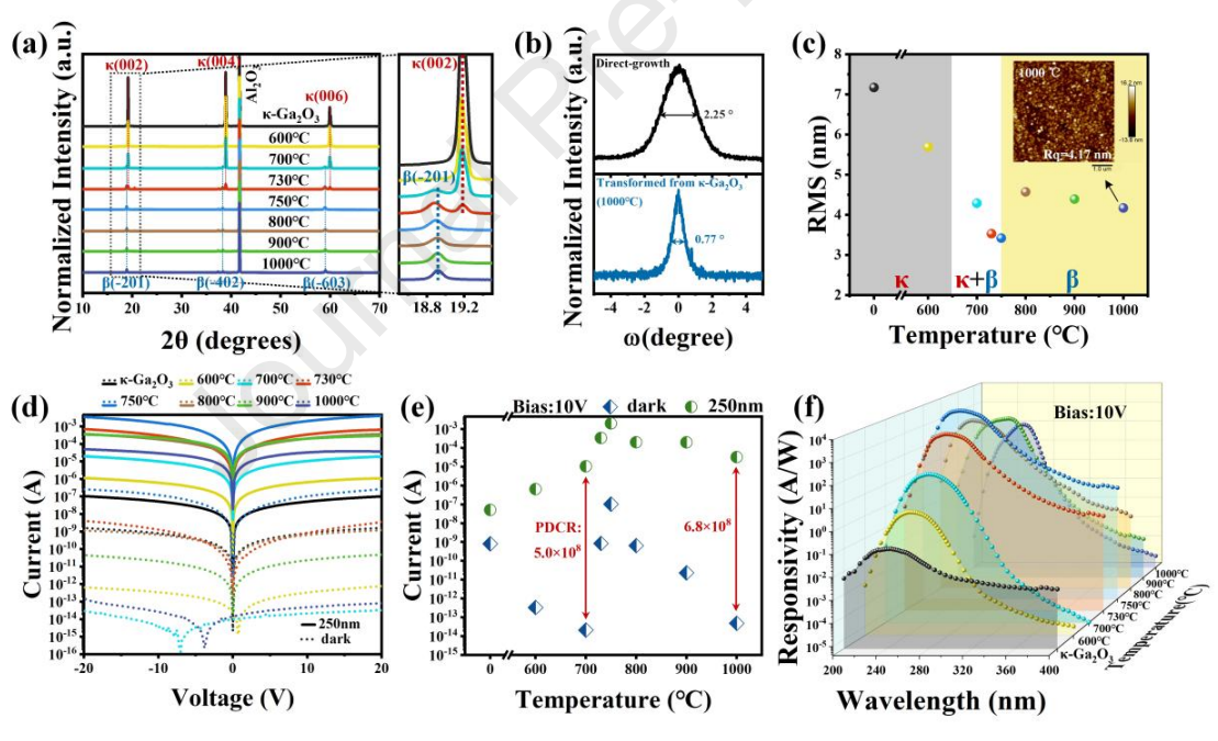
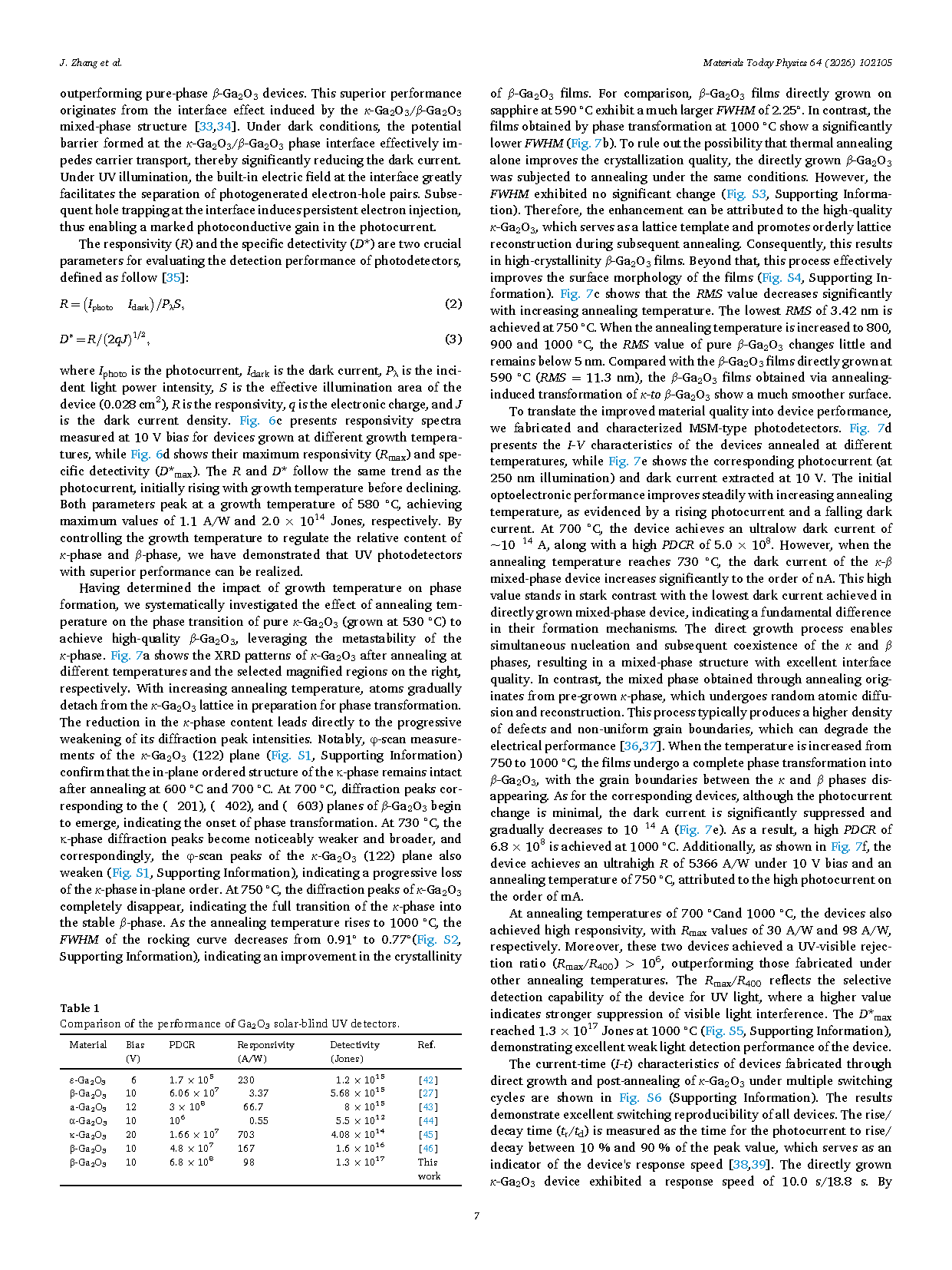
Figure 7. Effects of post-annealing temperature on κ‑Ga₂O₃ films and devices. (a) XRD patterns of films annealed at different temperatures (right panel: magnified view). (b) Comparison of XRD rocking curves of the β‑Ga₂O₃ (-201) plane between Ga₂O₃ phase-transformed after 1000 ℃ annealing and Ga₂O₃ directly epitaxially grown at 590 ℃. (c) RMS versus annealing temperature. (d) I–V characteristics of an MSM photodetector in the dark and under 250 nm illumination. (e) Photocurrent (under 250 nm illumination) and dark current at 10 V versus annealing temperature. (f) Response spectra at 10 V.
DOI:
doi.org/10.1016/j.mtphys.2026.102105