Paper Sharing
【Member Papers】 Electric field-directed anisotropic failure of β-Ga₂O₃
日期:2026-04-30阅读:237
Researchers from the Xidian University have published a dissertation titled " Electric field-directed anisotropic failure of β-Ga₂O₃" in Applied Physics Reviews.
Background
β-Gallium oxide (β-Ga₂O₃) is regarded as one of the most promising ultra-wide bandgap semiconductors for next-generation high-voltage power devices, owing to its ultra-high critical breakdown electric field (~8 MV/cm), large Baliga’s figure of merit, and stable material properties. However, during actual operation, power devices based on β-Ga₂O₃ inevitably endure long-term cyclic electrical stress and high-temperature thermal stress. Due to the intrinsic low thermal conductivity and strong structural anisotropy of β-Ga₂O₃, the coupling of electric field and thermal field will lead to severe uneven heat accumulation and localized electric field enhancement, which greatly reduces the service stability and long-term reliability of the device. Traditional reliability studies mostly focus on the evolution of macroscopic electrical parameters, and lack direct atomic-scale real-time observation and quantitative analysis of the structural failure process. In addition, the key driving force, microscopic mechanism, and evolutionary path of β-Ga₂O₃ failure under electro-thermal coupling conditions are still unclear, which severely restricts the performance optimization and reliability design of high-power β-Ga₂O₃ devices.
Highlights
The electric-field-directed anisotropic failure of β-Ga₂O₃ along (200) low-index planes under electro-thermal coupling fields is observed in real time at the atomic scale for the first time.
Decoupling experiments confirm that the electric field is the key driving force for anisotropic melting, while thermal and irradiation fields play auxiliary roles.
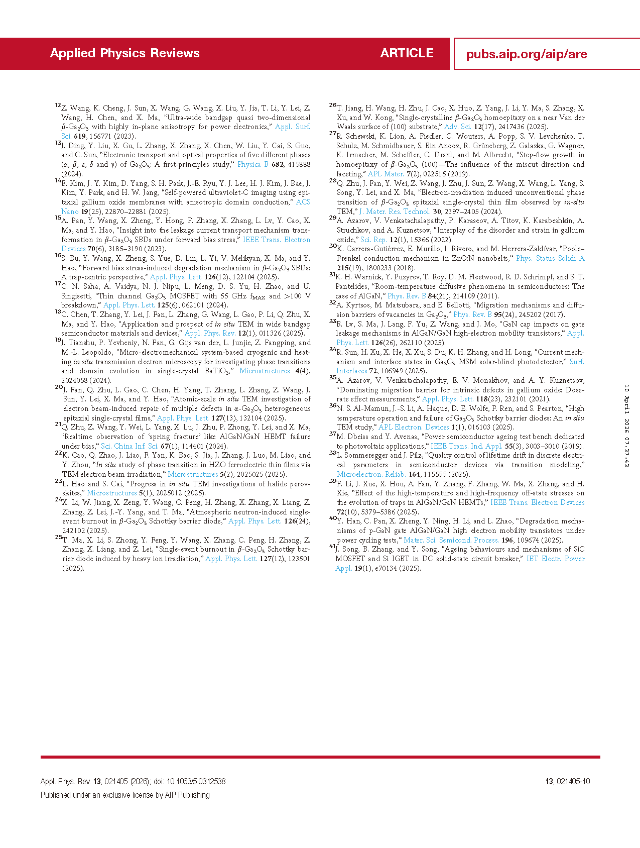
Two distinct melting mechanisms, layer-by-layer decomposition and multi-layer symmetric melting, are revealed on the (200) crystal plane of β-Ga₂O₃.
The melting rate increases by more than 4 times after electro-thermal aging, proving that cumulative stress causes irreversible structural degradation.
A complete physical chain of defect dynamics, electric field localization, and intrinsic anisotropy inducing anisotropic failure is established.
Conclusion
This work employed in situ TEM to reveal and elucidate for the first time an electric-field-directed anisotropic failure mechanism in β-Ga₂O₃ under multi-field coupling. The main conclusions are as follows: 1. The team discovered a novel mode of electric-field-driven anisotropic failure. The failure of β-Ga₂O₃ does not occur randomly, but strictly follows a highly ordered process along low-index planes such as (200), evolving from layer-by-layer delamination to multiple layers decomposition. Controlled decoupling experiments confirmed that the electric field is the key driving force triggering and guiding the anisotropic failure. 2. The team revealed the physical chain of anisotropic failure. Irradiation and electric fields synergistically introduced active vacancy defects; the electro-thermal fields synergistically defined the weak regions of the material; thermal conductivity dictated the path of anisotropic failure. Ultimately, anisotropic failure phenomena were triggered under multi-field coupling. 3. The team established an accelerated aging research paradigm at the micro/nanoscale, elucidating the accelerating effect of cumulative electro-thermal stress on β-Ga₂O₃ microstructural failure. After undergoing multiple electro-thermal stress, the melting rate of β-Ga₂O₃ material along the (200) plane increased by more than four times, revealing the intrinsic laws by which electro-thermal aging accelerates material failure evolution. 4. The team provides a theoretical basis and optimization strategies for the design of high-reliability β-Ga₂O₃ power devices. At the material level, suppressing the generation and migration of harmful point defects through defect engineering, while avoiding mechanical weak planes from the wafer fabrication stage to enhance intrinsic reliability. At the device level, synergistic optimization of channel orientation and electric field distribution can be achieved by aligning them along the optimal combination of thermal conductivity and breakdown electric field directions. This approach avoids anisotropic failure, enabling long-term stable operation of devices under service conditions. This work reveals the anisotropic failure mechanism of β-Ga₂O₃ under multi-field coupling from the atomic scale, expanding the perspective of wide bandgap semiconductor reliability research from macroscopic performance degradation to the microscopic level of crystal structure instability, and it provides crucial theoretical guidance for the future design of ultra-high-reliability β-Ga₂O₃-based power devices.
Project Support
National Natural Science Foundation of China (Grant Nos. 62274130, 62574157, and 62188102), the China Postdoctoral Science Foundation (Certificate No. 2024T170693), and the Tian Chi Ying Cai Project of Xinjiang Uygur Autonomous Region.

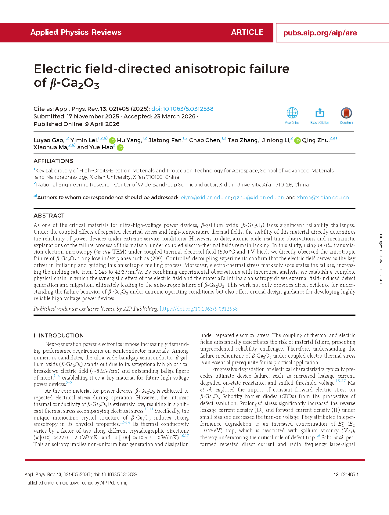
Figure 1 Anisotropic failure process of β-Ga₂O₃ at 500 °C, 1 V. (a)–(c) Schematic diagrams of the melting process. (d) Schematic illustration of the anisotropic melting evolution. (e)–(l) TEM images of the anisotropic melting process. (m) TEM image of the β-phase in the amorphous region and its corresponding FFT pattern.
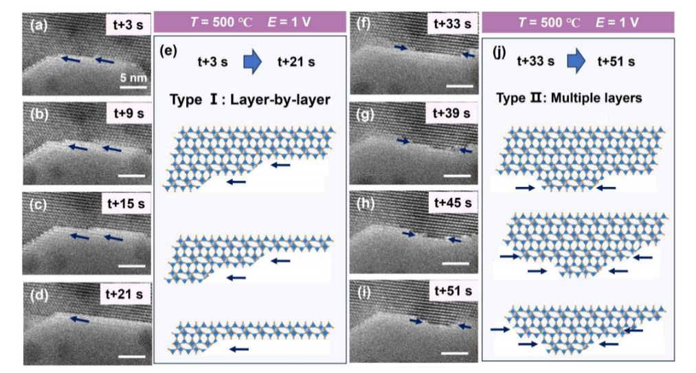
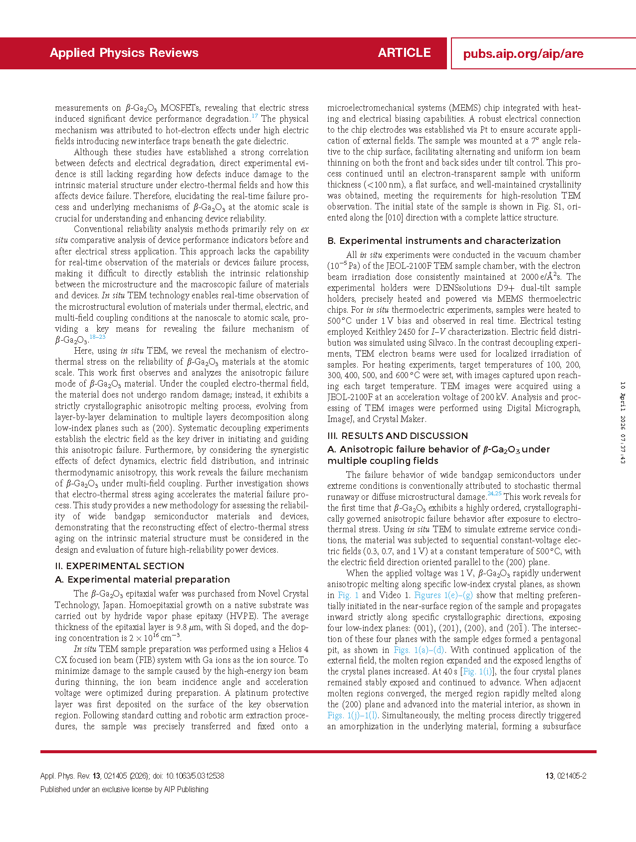
Figure 2 Two melting mechanisms on the β-Ga₂O₃ (200) crystal plane. (a)–(d) Type I: TEM images of the layer-by-layer melting process. (e) Schematic illustration of the layer-by-layer melting mechanism. (f)–(i) Type II: TEM images of the multiple layers melting process. (j) Schematic illustration of the multiple layers melting mechanism.
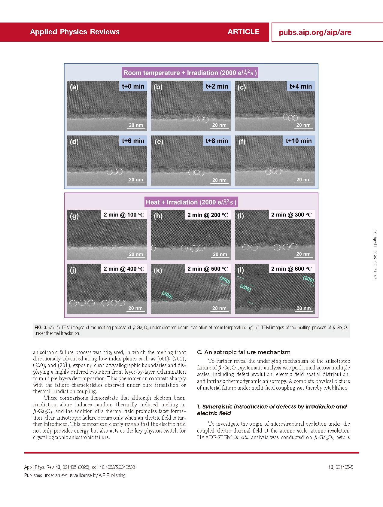
Figure 3 (a)–(f) TEM images of the melting process of β-Ga₂O₃ under electron beam irradiation at room temperature. (g)–(l) TEM images of the melting process of β-Ga₂O₃ under thermal irradiation.
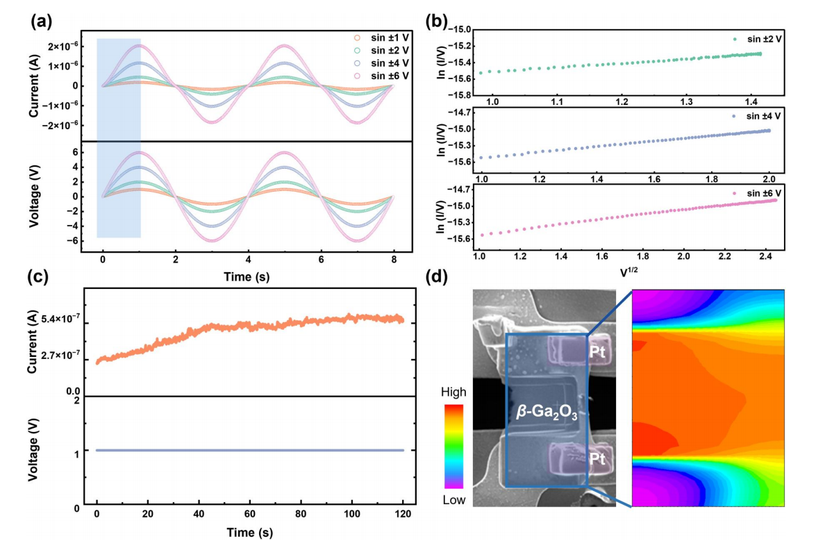
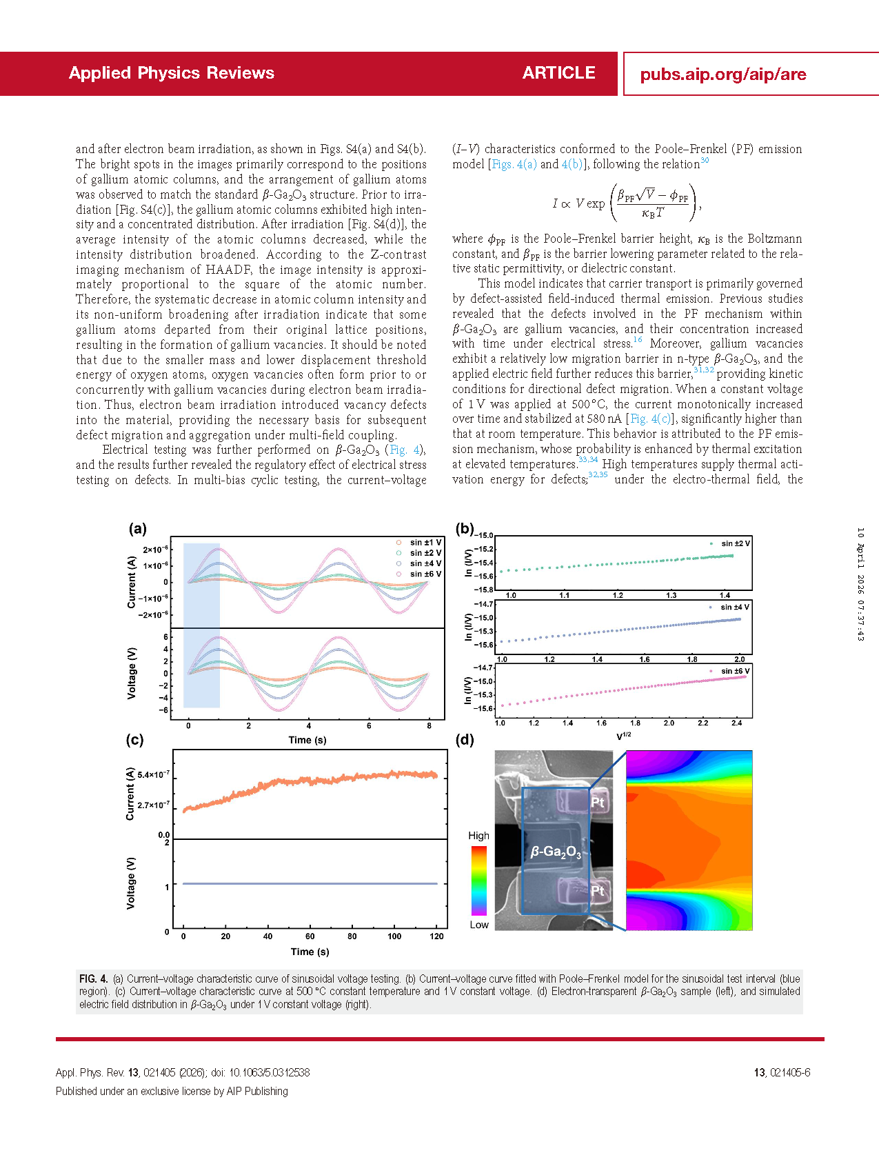
Figure 4 (a) Current–voltage characteristic curve of sinusoidal voltage testing. (b) Current–voltage curve fitted with Poole–Frenkel model for the sinusoidal test interval (blue region). (c) Current–voltage characteristic curve at 500 °C constant temperature and 1 V constant voltage. (d) Electron-transparent β-Ga₂O₃ sample (left), and simulated electric field distribution in β-Ga₂O₃ under 1 V constant voltage (right).
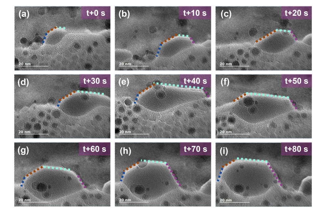
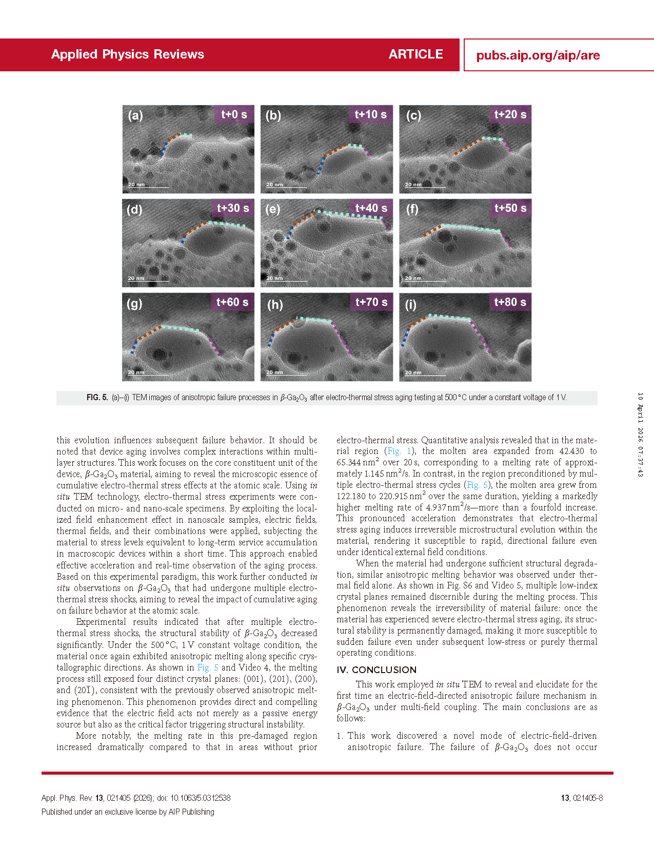
Figure 5 (a)–(i) TEM images of anisotropic failure processes in β-Ga₂O₃ after electro-thermal stress aging testing at 500 °C under a constant voltage of 1 V.
DOI :
doi.org/10.1063/5.0312538