Paper Sharing
【Domestic Papers】Amorphous-Ga₂O₃/CuₓO/Cu heterojunction for cost-effective weak-UV light detection
日期:2026-05-12阅读:4
Researchers from Songshan Lake Materials Laboratory and Dongguan Institute of Materials Science and Technology have published a dissertation titled " Amorphous-Ga2O3/CuxO/Cu heterojunction for cost-effective weak-UV light detection " in Journal of Physics D: Applied Physics.
Background
Solar-blind ultraviolet photodetectors (SBUV PDs) are sensitive to photons with wavelengths shorter than 280 nm, a spectral region in which solar radiation is strongly absorbed by the Earth's atmosphere. This feature endows SBUV PDs with low background noise and low false alarm rate, significantly favoring fire detection, space communication, and fast imaging etc. To obtain a compact filter-free detector, wide bandgap semiconductors such as AlGaN, MgZnO, diamond and Ga2O3, have been widely explored as the core photoelectron conversion materials. Ga2O3 is one of the most promising candidates considering its suitable bandgap (4.6 ~ 5.3 eV), excellent chemical stability and high breakdown electric field (8 MV·cm-1). Amorphous Ga2O3 (a-Ga2O3) has attracted growing attention because of its superior deep ultraviolet (UV) photoresponse ability. More importantly, the above-mentioned a-Ga2O3 thin films can be easily prepared on almost any substrates with merits of low cost and large scalability, revealing an inexpensive pathway for the development of high-performance SBUV PDs. Great efforts have been paid to further enhance the photoresponse behavior of a-Ga2O3. Various strategies, such as construction of VO-rich a-Ga2O3/VO-poor a-Ga2O3 double layers and three-terminal phototransistor architectures, have achieved high photoresponsivity (>hundreds of A·W-1) and fast response speed (<tens of ms), showing great potential for practical applications.
Abstract
Amorphous Ga2O3 (a-Ga2O3) has been attracting increasing attention in solar-blind ultraviolet (UV) photodetection, with advantages of appropriate bandgap, superior photoresponsivity, and ease of large-area homogeneous fabrication with low cost. To realize a low dark current and a high sensitivity, a high-quality Schottky contact is highly desirable. Despite the high work function and preferable contact behavior of noble Au metal, its high price and long-term instability significantly impede its potential applications. Here, an earth-abundant Cu metal is demonstrated as an effective electrode for high-performance a-Ga2O3 photodetectors with cost efficiency. An apparently lower dark current (~0.15 nA) and similarly high photocurrent (1.3 mA) are achieved by using Cu contact, leading to a high responsivity (2.3 × 10⁴ A·W-1) and detectivity (1.0 × 10¹⁵ Jones). The photodetector hence manifests a capability to detect weak UV light with an intensity as low as 0.1 μW·cm-2. Depth-profile X-ray photoelectron spectroscopy measurement clearly reveals the spontaneous formation of a CuxO interfacial layer between Cu and a-Ga2O3 thin film through bottom-up oxidation, which plays an effective role in reducing the dark current and separating the photo-induced electron-hole pairs. It is believed that the successful construction of high-performance solar-blind UV photodetectors by using the economic a-Ga2O3 thin film and Cu metal will significantly promote their practical various applications in the future.
Conclusion
In summary, SBUV PDs based on a-Ga2O3 thin films were fabricated with Cu and A electrodes. The Cu-based photodetector exhibits a significantly reduced dark current and almost identical high photocurrent compared with those using Au electrodes, demonstrating superior detectivity and PDCR values. Depth-profile XPS confirm the formation of the interfacial CuxO layer, effectively suppressing the dark current without affecting photo-induced carriers transport. This work demonstrates that Cu metal can effectively behave as a high work function material like Au when deposited on oxide surfaces, providing a practical approach for developing low-cost, large-area, and highly sensitive SBUV PDs.
Project Support
This work was supported by the National Natural Science Foundation of China (Grants No. 12574218, 62174113, 12174275 and 62404146), and Guangdong Basic and Applied Basic Research Foundation (Grants No. 2023A1515140094 and 2023A1515110730).
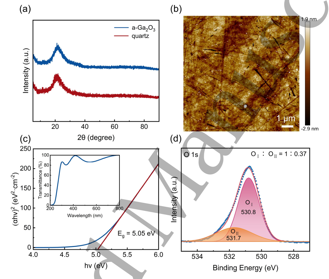
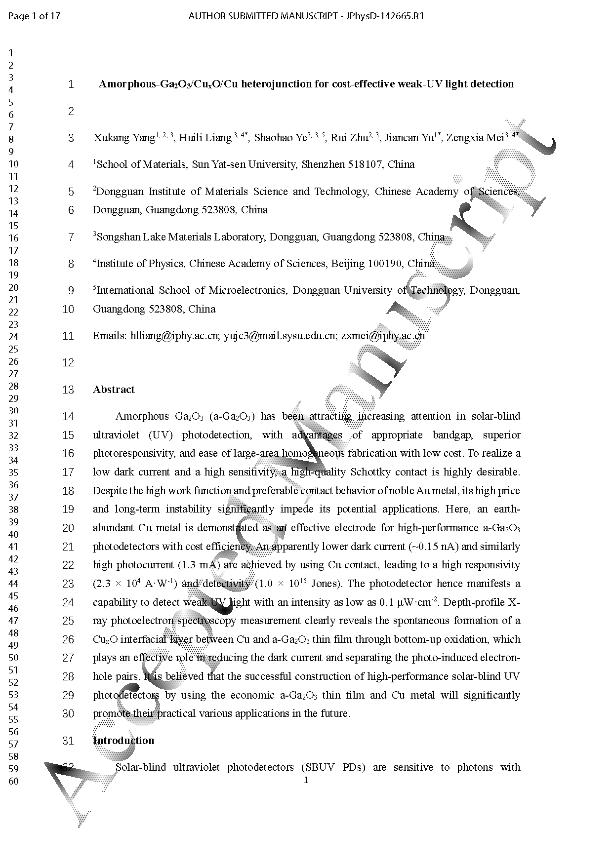
Figure 1. (a) XRD patterns of a-Ga2O3 film and quartz substrate. (b) AFM image of a-Ga2O3 thin film. (c) Tauc plot of a-Ga2O3 film (the inset is the optical transmittance spectrum). (d) The high resolution XPS spectrum of O1s for a-Ga2O3 film.
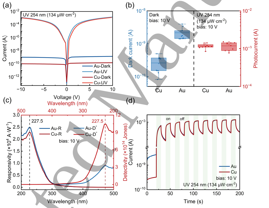
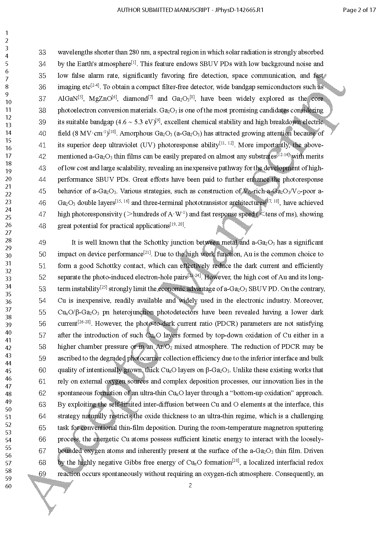
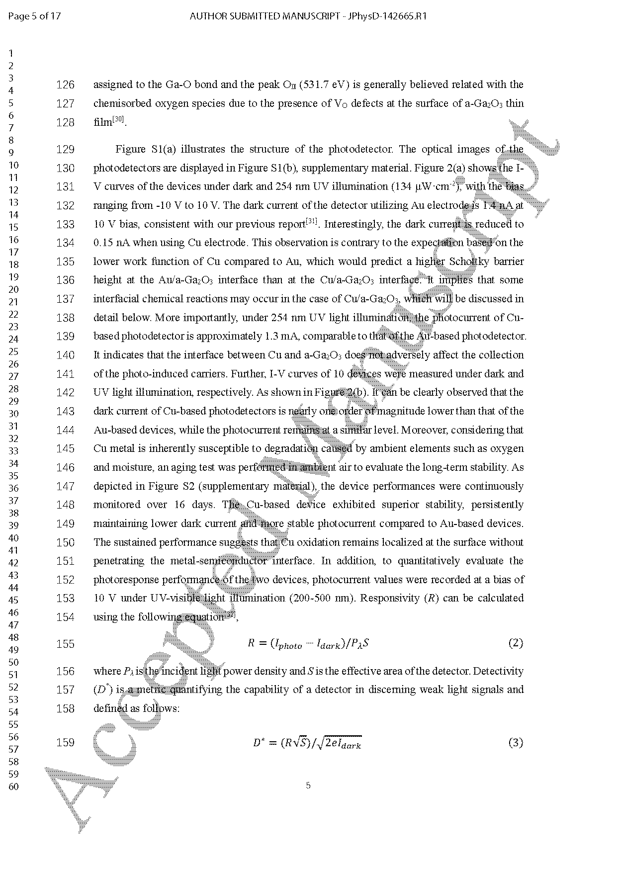
Figure 2. (a) The I-V characteristics of the PDs using Cu and Au electrodes under dark and 254 nm UV light illumination. (b) The histogram of the photocurrent and dark current values among 10 PDs using Au and Cu electrodes, respectively. (c) Responsivity and detectivity spectra for PDs with Au and Cu electrodes. (d) Time-dependent photocurrent curves biased at 10 V under periodic 254 nm UV light illumination.
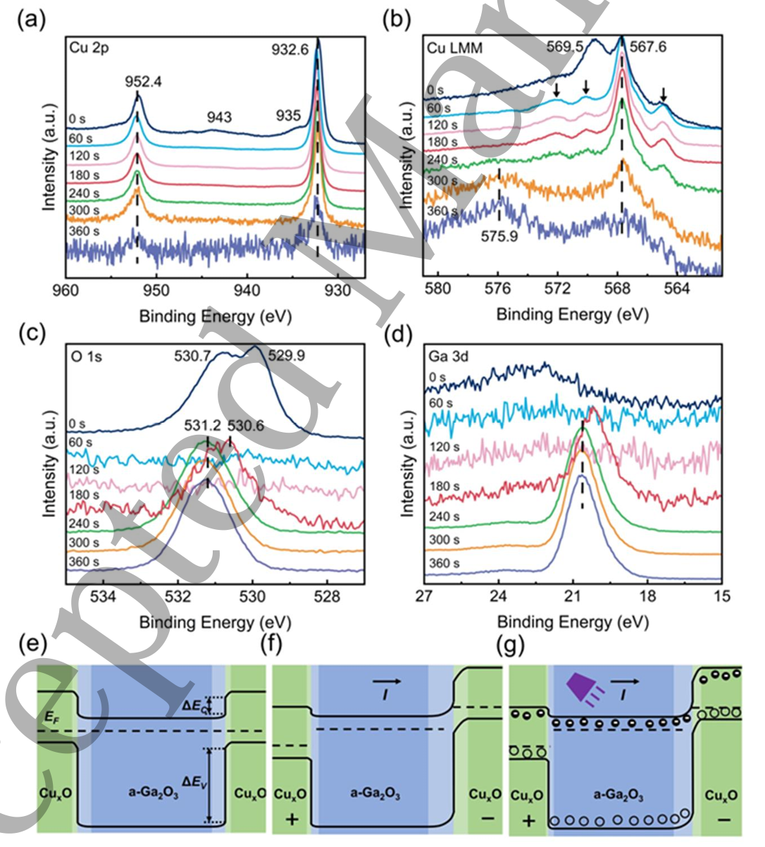
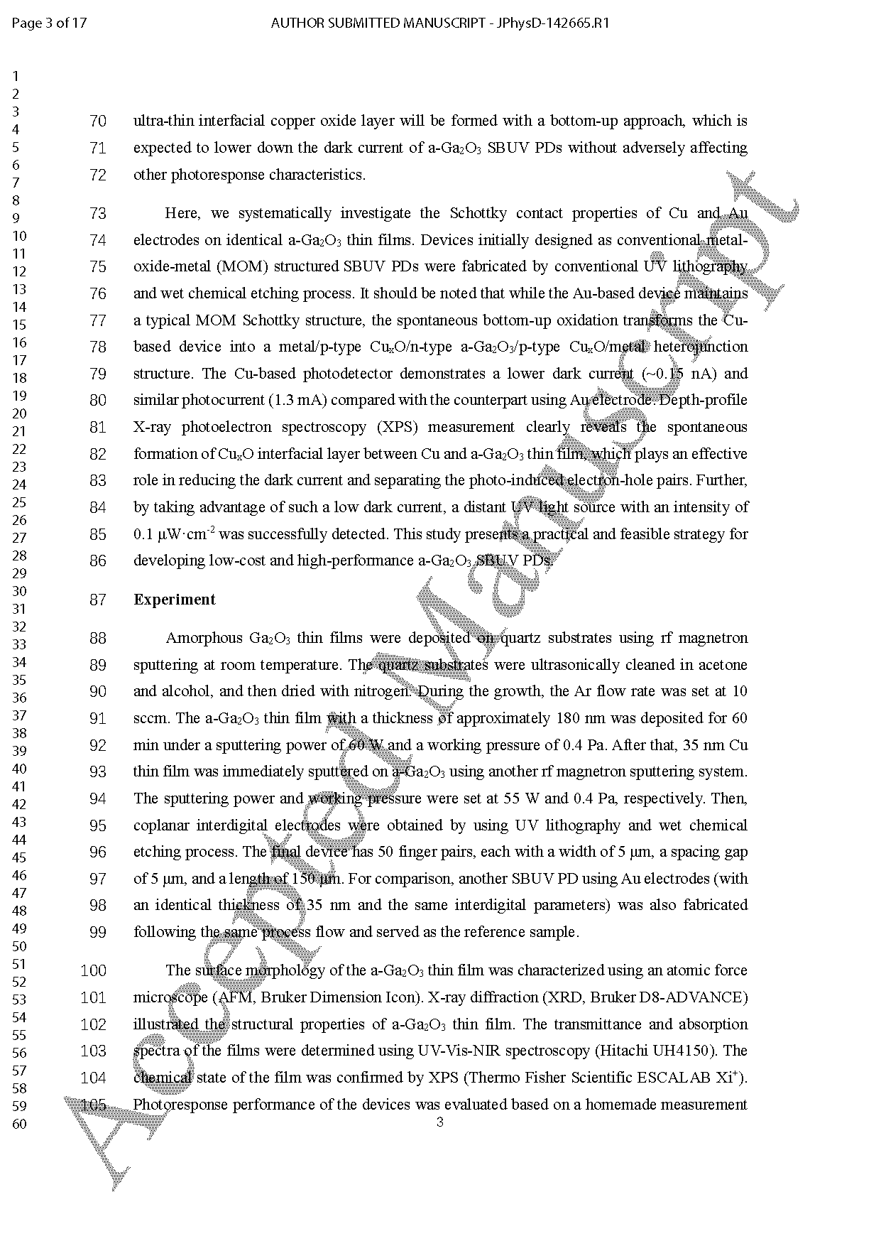
Figure 3. The high resolution XPS of (a) Cu 2p, (b) Cu LMM, (c) O 1s, (d) Ga 3d after different etching times. Schematic energy band diagrams of a-Ga2O3/CuxO heterojunction in the dark (e), under an external bias (f), under an external bias and UV light illumination (g).
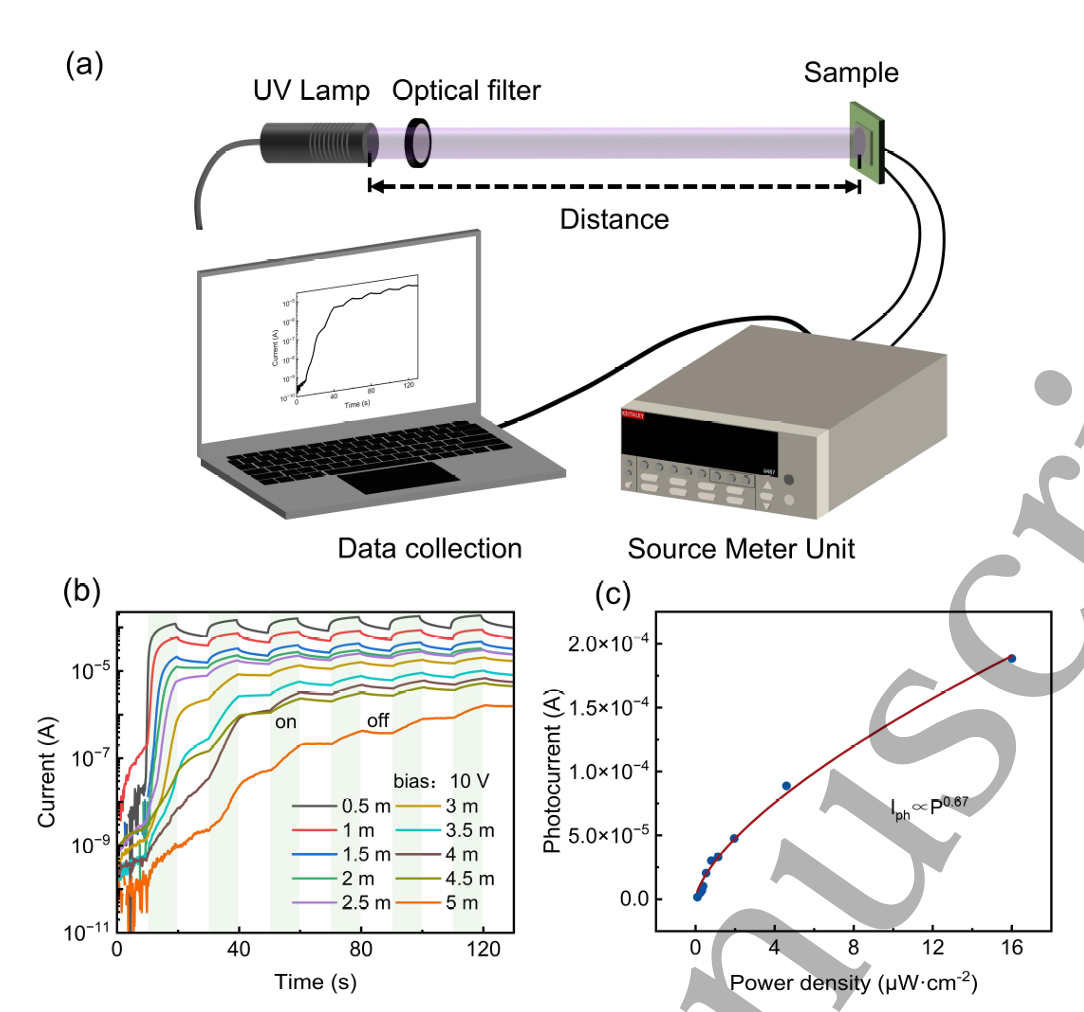
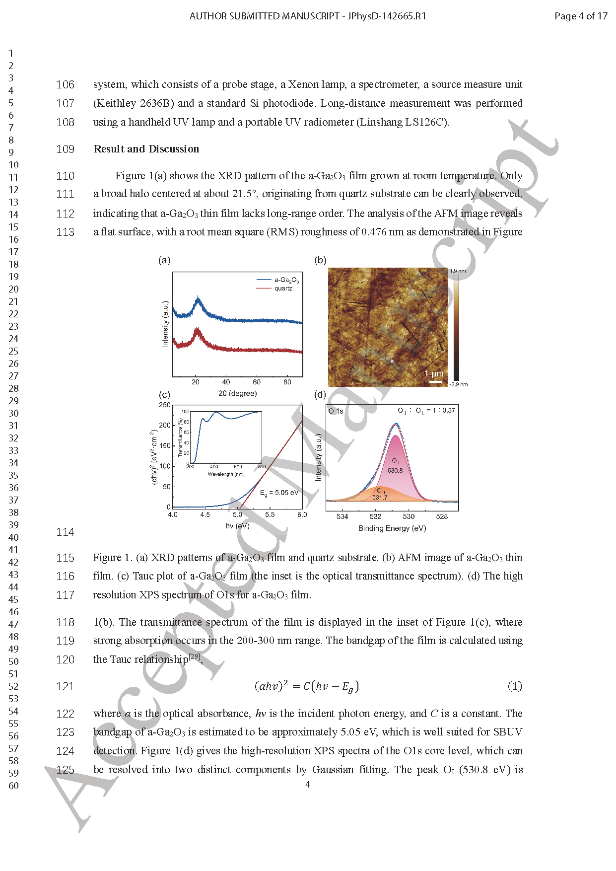
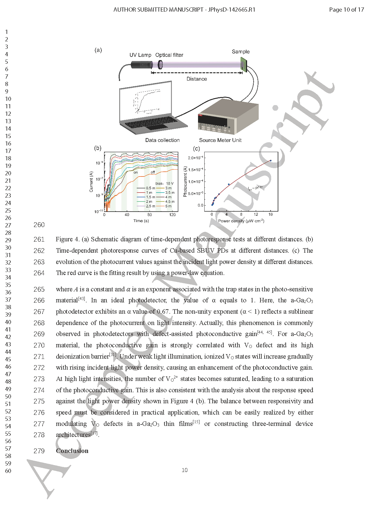
Figure 4. (a) Schematic diagram of time-dependent photoresponse tests at different distances. (b) Time-dependent photoresponse curves of Cu-based SBUV PDs at different distances. (c) The evolution of the photocurrent values against the incident light power density at different distances. The red curve is the fitting result by using a power-law equation.
DOI:
doi.org/10.1088/1361-6463/ae69f4