Paper Sharing
【Member Papers】High-performance vertical β-Ga₂O₃ Schottky barrier diodes utilizing sputtered p-NiO double mesa junction termination extension
日期:2026-05-12阅读:4
Researchers from the Xidian University, The 13th Research Institute of China Electronic Technology Group Corporation, University of Science and Technology of China have published a dissertation titled "High-performance vertical β-Ga₂O₃ Schottky barrier diodes utilizing sputtered p-NiO double mesa junction termination extension" in Journal of Vacuum Science & Technology A.
Background
Beta-gallium oxide (β-Ga₂O₃) has emerged as a promising candidate for next-generation power electronics, owing to its ultra-wide bandgap (∼4.8 eV) and a high theoretical breakdown field estimated at 8 MV/cm. These properties translate to Baliga’s figure of merit significantly surpassing that of SiC and GaN. Furthermore, the commercial availability of bulk substrates produced via melt-growth techniques, combined with the tunability of n-type doping, positions β-Ga₂O₃ as a superior candidate for high-quality homoepitaxy, paving the way for cost-effective device fabrication. However, maximizing the breakdown capability of β-Ga₂O₃ devices requires effective edge termination techniques to mitigate electric field crowding at the anode periphery, which typically leads to a premature breakdown well below the material limit. While various termination strategies have been explored, single-mesa structures often merely shift the peak electric field from the anode edge to the trench corners. Integrating a p-NiO junction termination extension (JTE) with the mesa has proven effective, but the potential of double-mesa architectures for ultra-wide bandgap β-Ga₂O₃ power rectifiers remains unexplored.
Abstract
Effective management of peak electric fields at the electrode edge poses a critical challenge in realizing the full potential of ultra-wide bandgap β-Ga₂O₃ power devices. In this work, we report on the fabrication and characterization of vertical β-Ga₂O₃ Schottky barrier diodes (SBDs) employing a termination structure designated as double-mesa junction termination extension (DMJTE), which is applied to vertical β-Ga₂O₃ devices for the first time. This design integrates a hierarchical dual-mesa architecture with a sputtered p-type NiO layer to provide a synergistic JTE-induced lateral depletion effect. The mesa geometry, comprising a 300 nm shallow step and a 1.5 μm deep trench, both formed using a BCl₃/Ar inductively coupled plasma etching process. Electrical characterization reveals that the DMJTE-SBD achieves a breakdown voltage (Vbr) of 2810 V. This breakdown voltage represents a substantial improvement over 590 V measured for the reference planar SBD (Ref-SBD) and 1530 V obtained for the single-mesa SBD with JTE (SMJTE-SBD). With a specific on-resistance of 6.9 mΩ·cm², the proposed DMJTE-SBD demonstrates a high power figure of merit of 1.14 GW/cm². TCAD simulations validate that the DMJTE topology effectively smooths the potential gradient and displaces the peak electric field away from the anode edge.
Highlights
The double-mesa junction termination extension (DMJTE) structure is proposed and applied to vertical β-Ga₂O₃ Schottky barrier diodes for the first time, combining a hierarchical dual-mesa architecture with a sputtered p-NiO layer for synergistic electric field regulation.
A BCl₃/Ar inductively coupled plasma etching process is used to precisely fabricate a dual-mesa structure with a 300 nm shallow step and a 1.5 μm deep trench. The p-NiO layer is prepared by optimized RF magnetron sputtering, and post-sputtering annealing repairs plasma-induced damage and improves interface quality.
The DMJTE-SBD achieves a breakdown voltage of 2810 V, 3.76 times higher than that of planar devices and 83.7% higher than that of single-mesa devices. Its power figure of merit reaches 1.14 GW/cm², far exceeding the theoretical limits of Si and 4H-SiC, leading among similar devices in the 2–3 kV range.
TCAD simulations confirm that the shallow step buffers the electric field, the deep trench disperses the electric field, and the p-NiO layer broadens the depletion region via the RESURF effect. Multiple effects suppress the peak electric field and avoid premature breakdown.
Conclusion
In summary, we have successfully designed and fabricated high-voltage vertical β-Ga₂O₃ SBDs by introducing a DMJTE architecture into this material system. The fabrication process integrated a precise ICP dry etching technique to form the hierarchical mesa and optimized reactive sputtering for p-NiO deposition. This combination effectively mitigated the electric field crowding at the anode edge and the mesa corners through a synergistic grading and RESURF effect. Consequently, the DMJTE-SBD demonstrated a breakdown voltage of over 2810 V and a PFOM of 1.14 GW/cm², significantly outperforming planar and single-mesa counterparts. These results highlight the potential of the DMJTE technology for advancing the performance of robust β-Ga₂O₃ power devices.
Project Support
This work was supported by the National Key Research and Development Program of China (No. 2024YFE0205200) and the NSFC under Grant Nos. 62404214, 62474170, U23A20358, and 62234007. This work was partially carried out at the Center for Micro and Nanoscale Research and Fabrication of USTC.
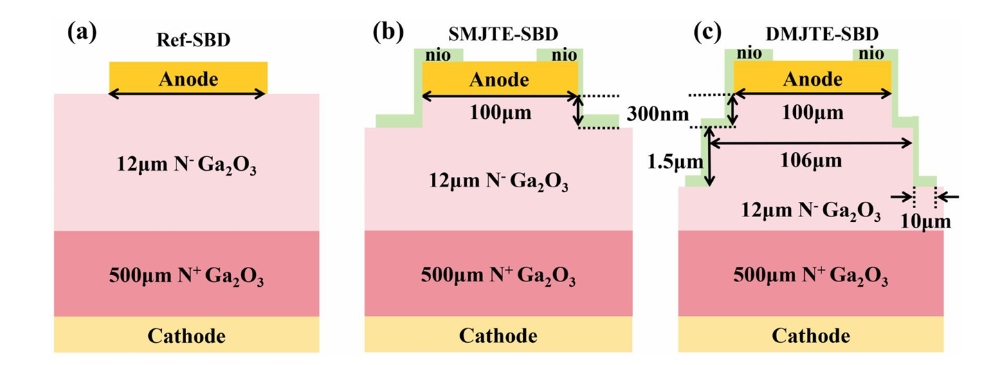
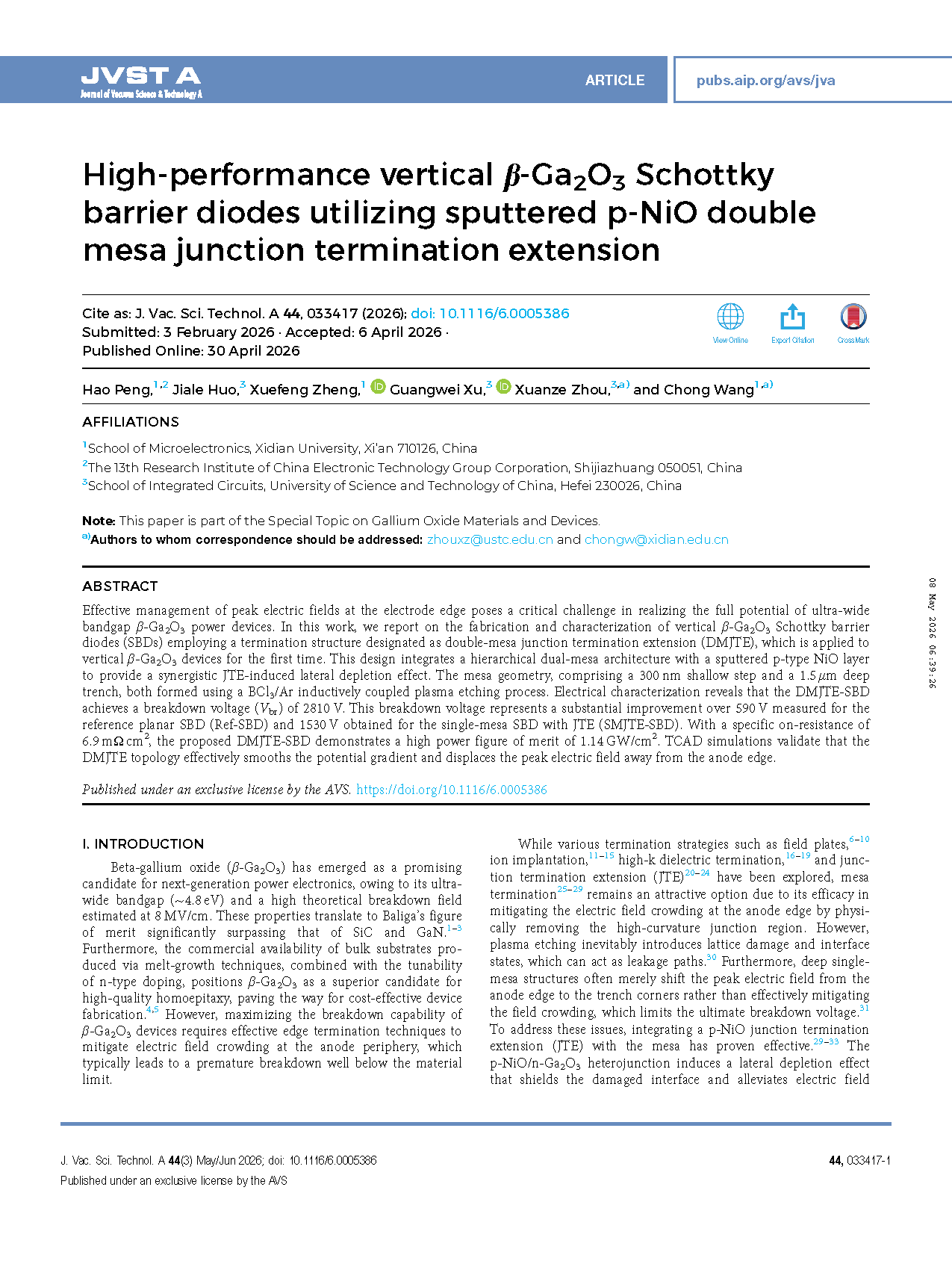
Figure 1 Schematic cross sections of the fabricated (a) Ref-SBD, (b) SMJTE-SBD, and (c) DMJTE-SBD.
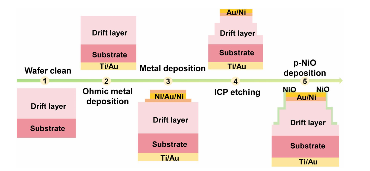
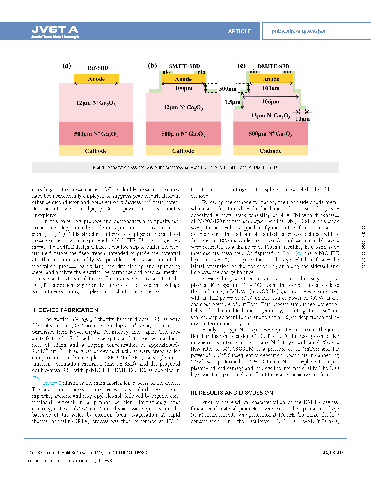
Figure 2 Fabrication details of the β-Ga₂O₃ SBD with DMJTE.
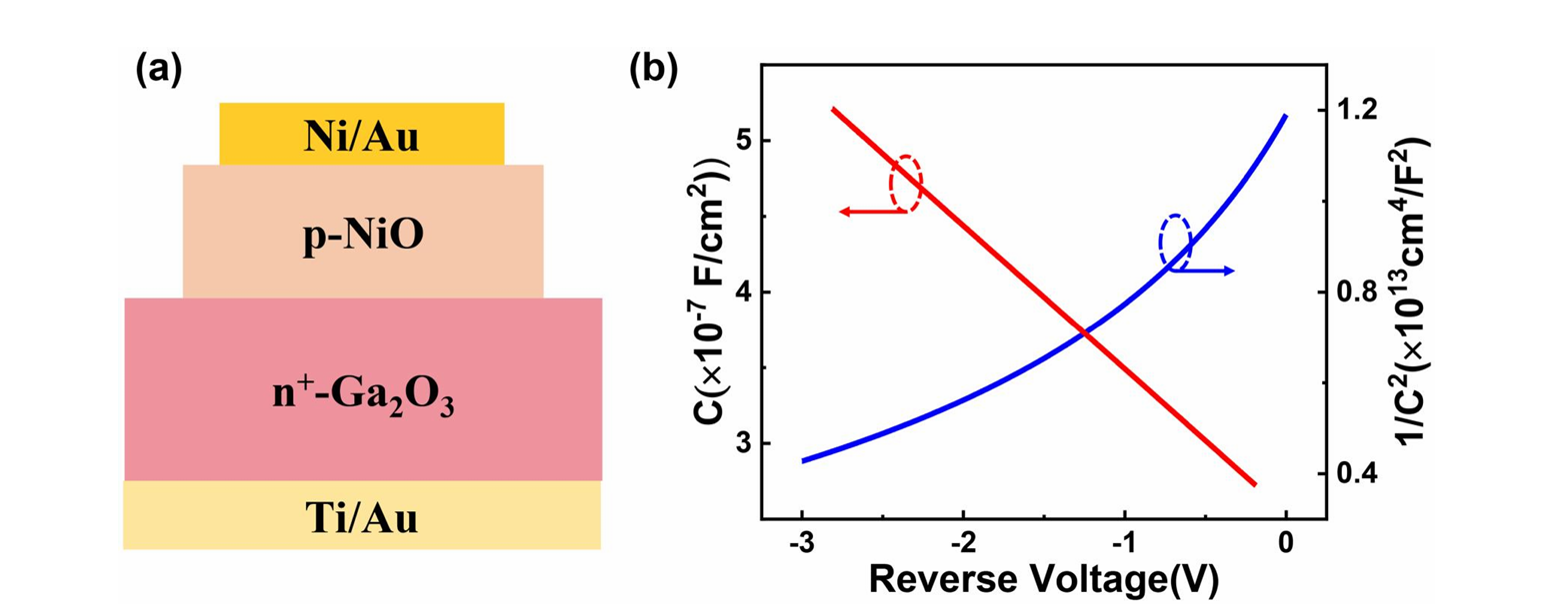
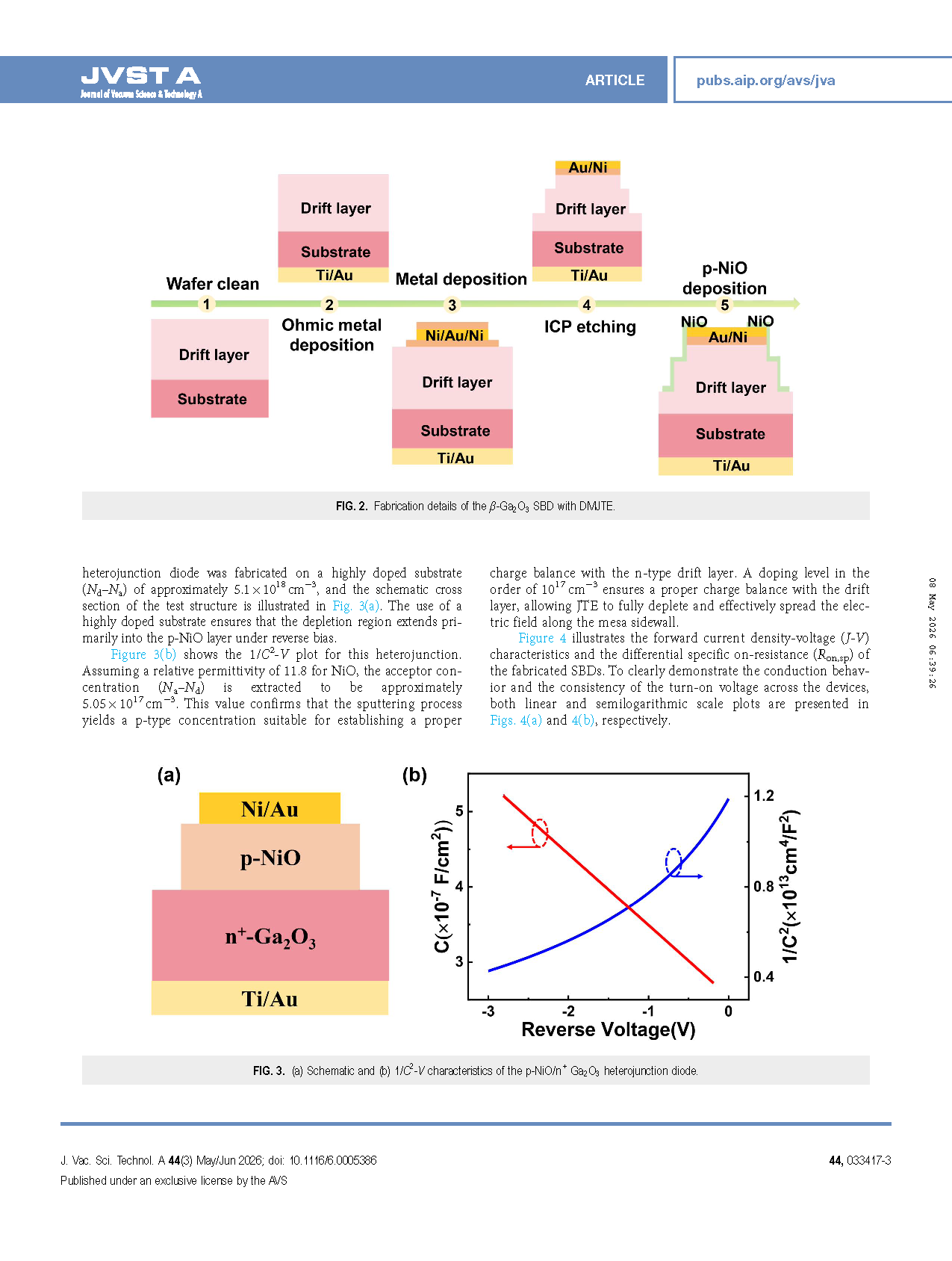
Figure 3 (a) Schematic and (b) 1/C²-V characteristics of the p-NiO/n⁺Ga₂O₃ heterojunction diode.

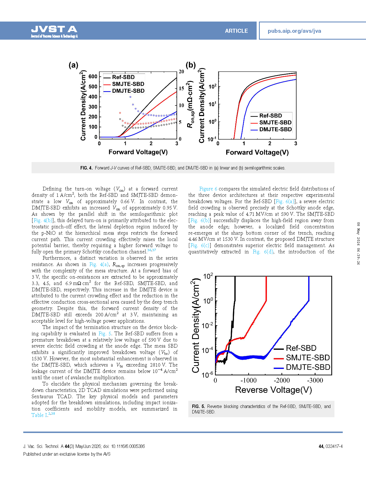
Figure 4 Forward J-V curves of Ref-SBD, SMJTE-SBD, and DMJTE-SBD in (a) linear and (b) semilogarithmic scales.
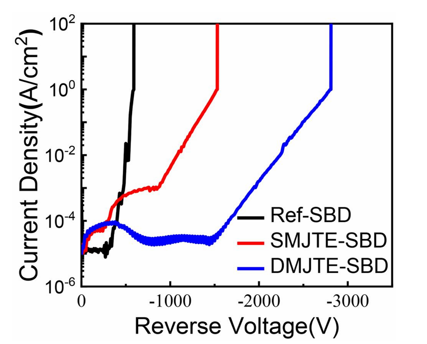
Figure 5 Reverse blocking characteristics of the Ref-SBD, SMJTE-SBD, and DMJTE-SBD.
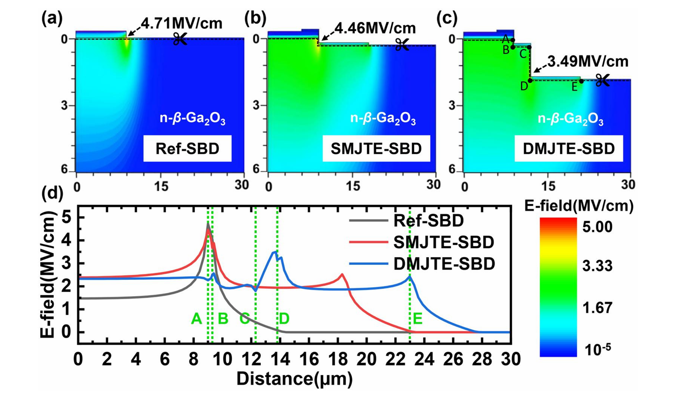
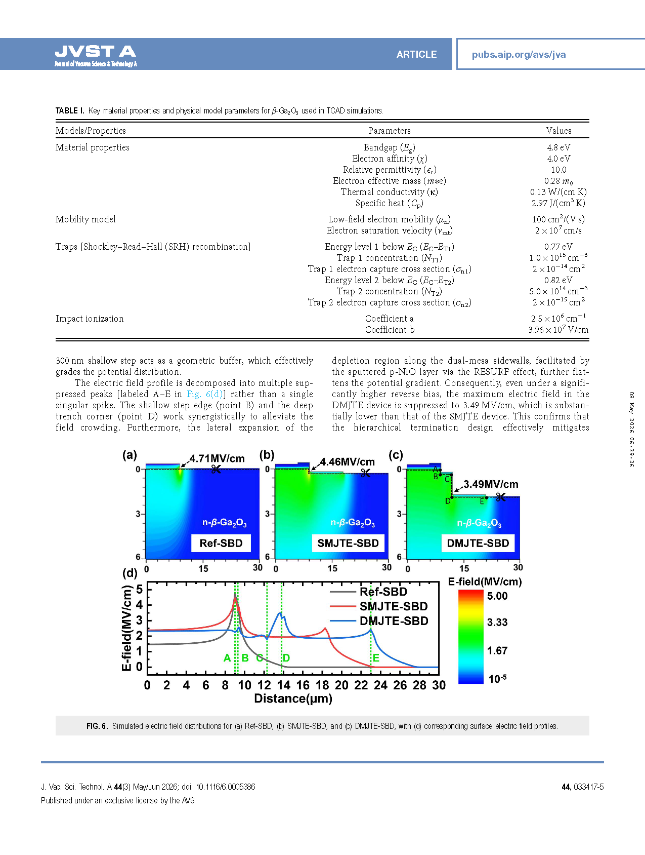
Figure 6 Simulated electric field distributions for (a) Ref-SBD, (b) SMJTE-SBD, and (c) DMJTE-SBD, with (d) corresponding surface electric field profiles.
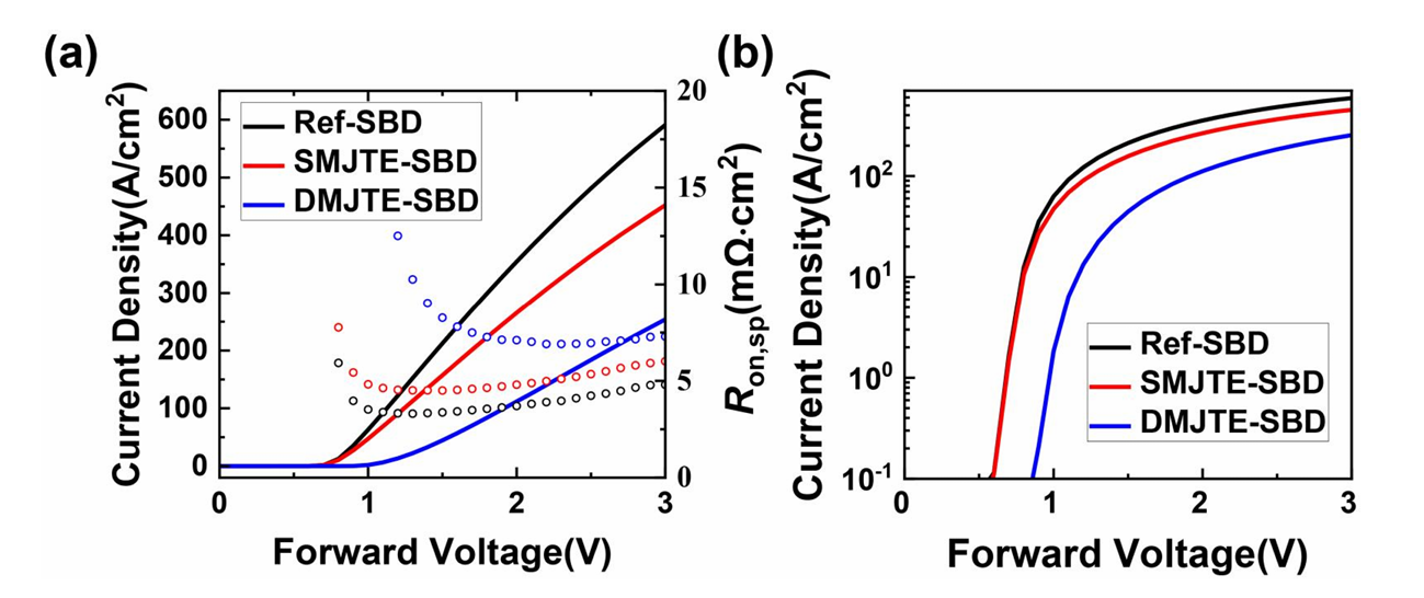
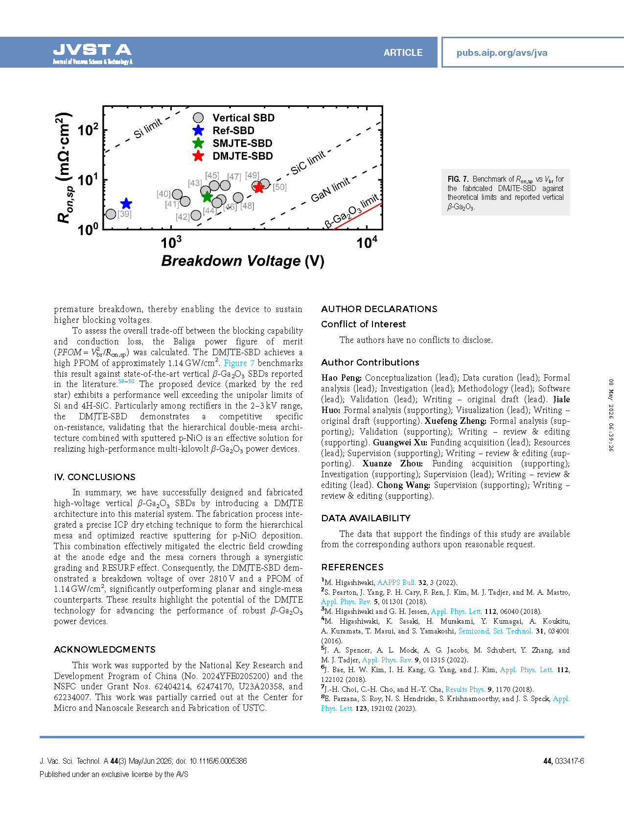
Figure 7 Benchmark of Rₒₙ,ₛₚ vs Vᵦᵣ for the fabricated DMJTE-SBD against theoretical limits and reported vertical β-Ga₂O₃ SBDs.
DOI:
10.1116/6.0005386