Paper Sharing
【International Papers】VBr >10 kV E-Beam/Sputtered Vertical NiOx/(011) β-Ga₂O₃ HJDs with PFOM >2.3 GW/cm²
日期:2026-05-12阅读:5
Researchers from the University of California and United States Naval Research Laboratory (NRL) have published a dissertation titled "VBr >10 kV E-Beam/Sputtered Vertical NiOx/(011) β-Ga₂O₃ HJDs with PFOM >2.3 GW/cm²".
Background
The rapid expansion of data centers for artificial intelligence (AI) and charging networks for electric vehicles (EVs) have stimulated the necessity for efficient, cost-effective grid-level transmission and power conversion circuits at medium voltage level (1-35 kV). Solid states transformers (SSTs) are critical for data centers in enabling efficient, high power density distribution by replacing conventional magnetic transformers with power semiconductor-based converters. Enormous market potential is available in direct-to-rack power conversion for AI data centers that facilitate large voltage (13.5-35 kV, AC) to 800 V DC to reduce immediate power conversion steps, improving efficiencies for AI graphics processing units (GPUs) and accelerators. The high critical electric field strength (6-8 MV/cm) and availability of the shallow hydrogenic dopants in epitaxial β-Ga2O3 can be leveraged to demonstrate power devices with much lower differential specific on-resistance while operating at a higher blocking voltage compared to silicon carbide (SiC) and gallium nitride (GaN). Although reliable p-type doping is currently not available in β-Ga2O3, heterojunctions formed with p-NiOx are able to realize multi-kV class junctions along with breakdown electric field anisotropy across various orientations.
Abstract
Beta-gallium oxide (β-Ga₂O₃) holds enormous potential for medium voltage range power electronic applications. This work reports VBr > 10 kV/Ron,sp = 43 mΩ•cm2 class edge terminated vertical heterojunction diodes (HJDs) with e-beam/sputtered nickel oxide (NiOx) stack on epitaxial (011) β-Ga₂O₃. The power figure of merit (PFOM) of the HJD exceeds 2.3 GW/cm2. The extracted parallel plane breakdown field is > 5.3 MV/cm, which is the highest reported electric field for thick (011) β-Ga₂O₃ epitaxial drift layer.
Conclusion
This work demonstrates >10 kV class NiOx/(011) HVPE β-Ga₂O₃ heterojunction diodes by combining e-beam and sputtered NiOx as the p-type layers. The field-plated HJD with mesa-isolation accomplishes a PFOM value > 2.3 GW/cm2 and a parallel-plane breakdown electric field > 5.3 MV/cm. The high breakdown voltage/electric field accomplished on (011) β-Ga₂O₃ along with large PFOM value suggests this substrate orientation possesses potential for high electric field handling capability.
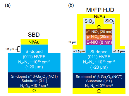
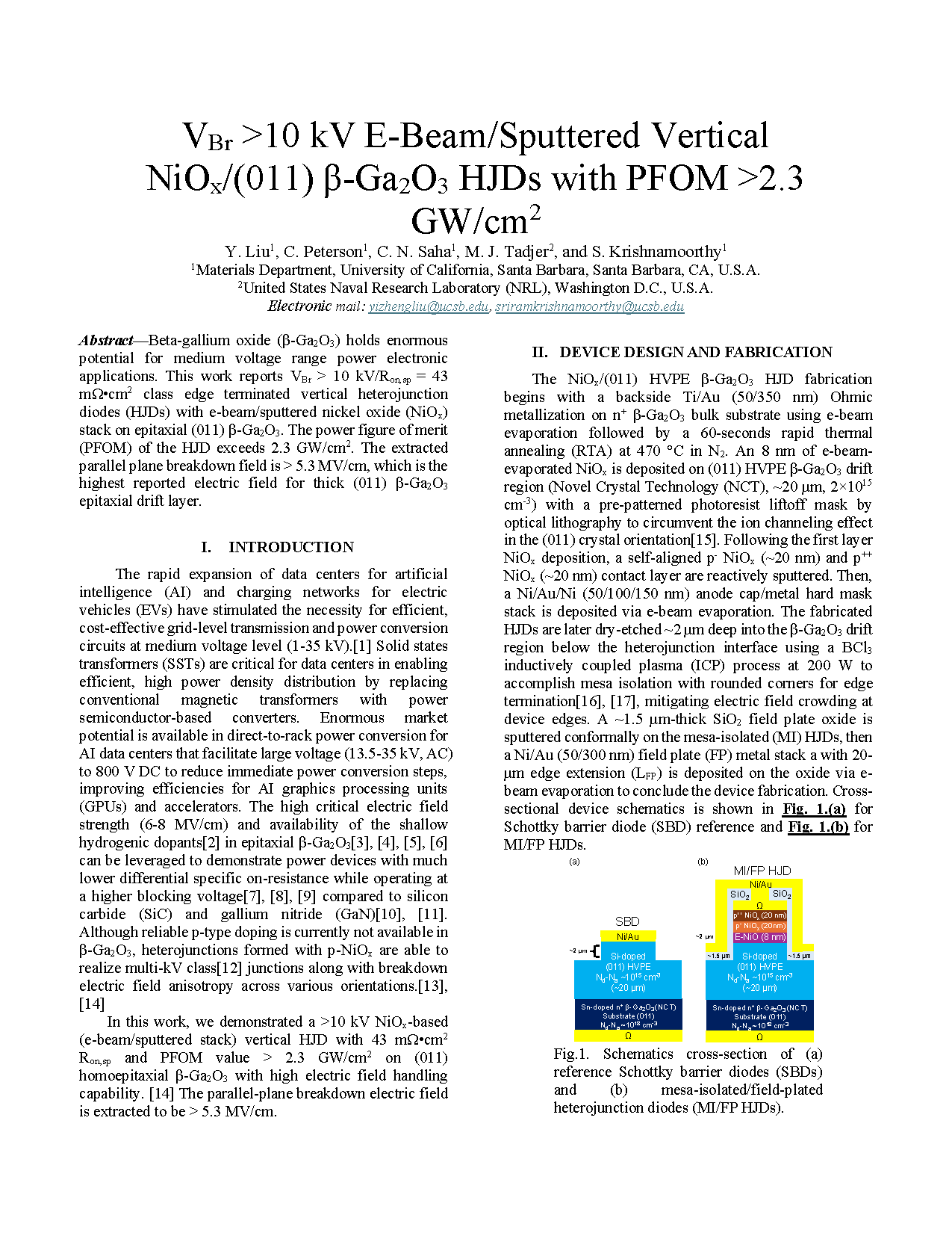
Fig.1. Schematics cross-section of (a) reference Schottky barrier diodes (SBDs) and (b) mesa-isolated/field-plated heterojunction diodes (MI/FP HJDs).
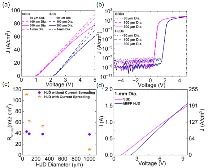
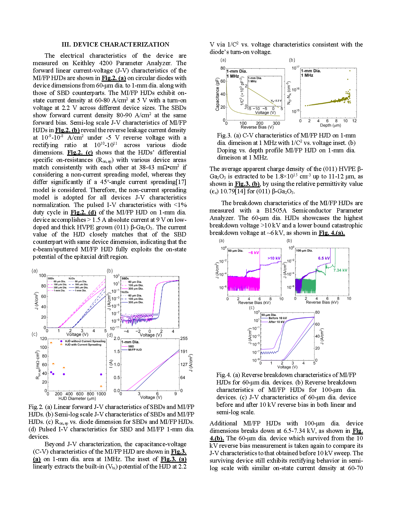
Fig.2. (a) Linear forward J-V characteristics of SBDs and MI/FP HJDs. (b) Semi-log scale J-V characteristics of SBDs and MI/FP HJDs. (c) Ron,sp vs. diode dimension for SBDs and MI/FP HJDs. (d) Pulsed I-V characteristics for SBD and MI/FP 1-mm dia. devices.
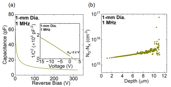
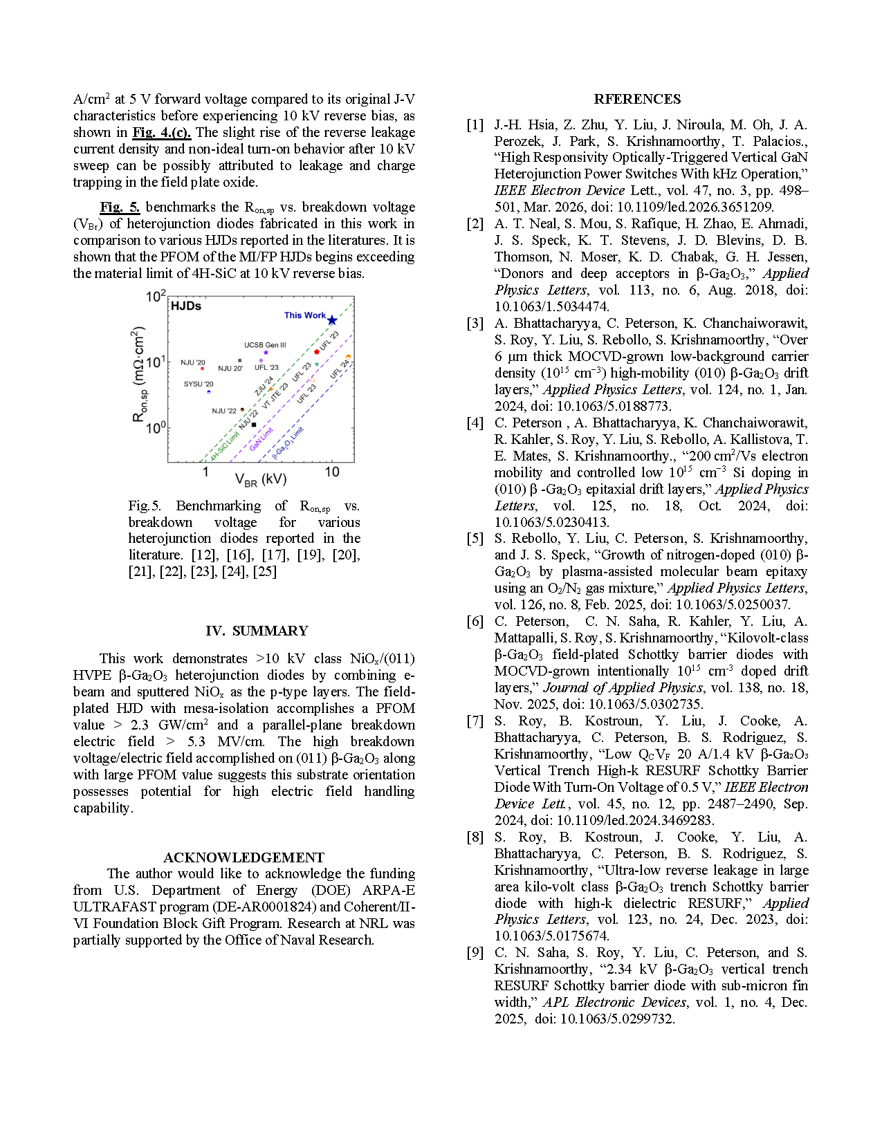
Fig.3. (a) C-V characteristics of MI/FP HJD on 1-mm dia. dimeison at 1 MHz with 1/C2 vs. voltage inset. (b) Doping vs. depth profile MI/FP HJD on 1-mm dia. dimeison at 1 MHz.
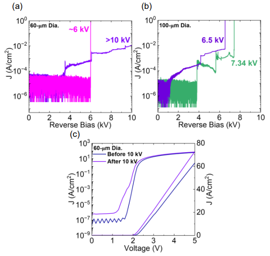
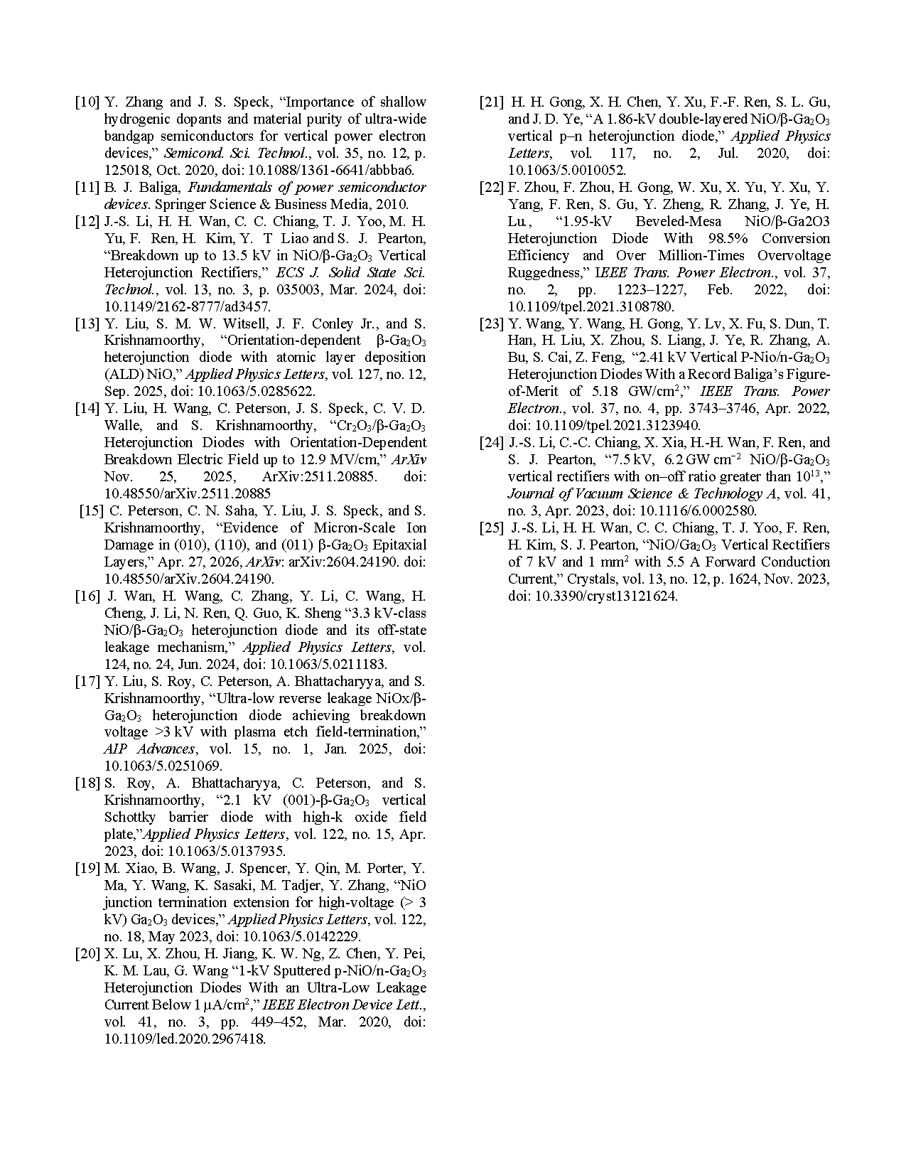
Fig.4. (a) Reverse breakdown characteristics of MI/FP HJDs for 60-μm dia. devices. (b) Reverse breakdown characteristics of MI/FP HJDs for 100-μm dia. devices. (c) J-V characteristics of 60-μm dia. device before and after 10 kV reverse bias in both linear and semi-log scale.
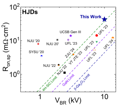
Fig.5. Benchmarking of Ron,sp vs. breakdown voltage for various heterojunction diodes reported in the literature.
DOI:
doi.org/10.48550/arXiv.2604.27262