Paper Sharing
【Member Papers】Impact of Miscut Angles on Mechanical Properties and Surface Damage of (100) β-Ga₂O₃
日期:2026-05-19阅读:158
Researchers from the Zhejiang University have published a dissertation titled " Impact of Miscut Angles on Mechanical Properties and Surface Damage of (100) β-Ga₂O₃" in Semiconductor Science and Technology.
Background
β‑Ga₂O₃ is an emerging ultra‑wide‑bandgap semiconductor with a bandgap of ~4.9 eV and a theoretical breakdown field strength up to 8 MV/cm. It can be grown into large‑size bulk single crystals at low cost via melt methods, showing great potential in power electronics and optoelectronic devices. The (100) plane facilitates large‑diameter scaling and serves as the main orientation for 8‑inch β‑Ga₂O₃ single crystals, with excellent ohmic contact properties. However, homoepitaxy on the (100) plane is prone to twin lamellae defects. Introducing miscut angles can transform the growth mode from 2D islands to step‑flow and improve epitaxial quality, yet the effects of miscut angles on the mechanical properties, processing surface damage and subsurface defects of (100) β‑Ga₂O₃ remain unclear. Wafer processing such as slicing, grinding and polishing inevitably introduces surface and subsurface damage, which directly degrades epitaxial quality and device performance. Therefore, a systematic study on the mechanical behavior and surface integrity of substrates with different miscut angles is critical for optimizing substrate processing and supporting high‑performance device fabrication.
Abstract
β-Ga₂O₃ is an emerging ultra-wide-bandgap semiconductor material with significant potential for power and optoelectronic devices. High-quality homoepitaxial growth plays a critical role in its device performance. While miscut angles on (100)-oriented substrates have been shown to promote step-flow mode in epitaxial growth methods such as MOCVD, their effects on mechanical properties and surface damage behavior remain unclear. In this study, β-Ga₂O₃ (100) substrates with miscut angles of 0°, 4°, and 6° were systematically investigated using nanoindentation, TEM, AFM, and wet chemical etching. The result indicates that the 6° miscut substrate exhibits a reduction in hardness by approximately 13%, to 8.31±0.36 GPa compared to ~9.57–9.78 GPa for 0° and 4°substrates. In contrast, the elastic modulus increases with bigger miscut angle. Under 1 mN load, both the 4° and 6° samples primarily deform via dislocations and stacking faults. The 4° miscut sample additionally shows the formation of an amorphous layer (α-phase regions), and near-surface (200) stacking faults. Surface morphology analysis reveals brittle removal with cleavage pits in 4° miscut substrate, whereas the 6° sample demonstrates ductile removal and lower defect density. These findings underscore the important influence of miscut angle on the mechanical response and surface integrity of β-Ga₂O₃ substrates. Providing insights for optimizing epitaxial growth and enhancing device performance.
Highlights
The regulation law of miscut angles on hardness and elastic modulus of (100) β‑Ga₂O₃ substrates is systematically revealed for the first time. 6° miscut reduces hardness by 13% and increases elastic modulus.
Different deformation mechanisms are found in 4° and 6° miscut substrates: 4° accompanies amorphous layer, α phase transformation and (200) stacking faults, while 6° is dominated by plastic deformation with simpler defects.
Miscut angle determines the processing removal mode: 4° is brittle removal with cleavage pits, and 6° is ductile removal with lower surface and subsurface defect density.
The correlation between miscut angle‑mechanical properties‑surface damage‑epitaxial quality is established, providing direct experimental basis for optimizing β‑Ga₂O₃ substrate processing and epitaxial technology.
Conclusion
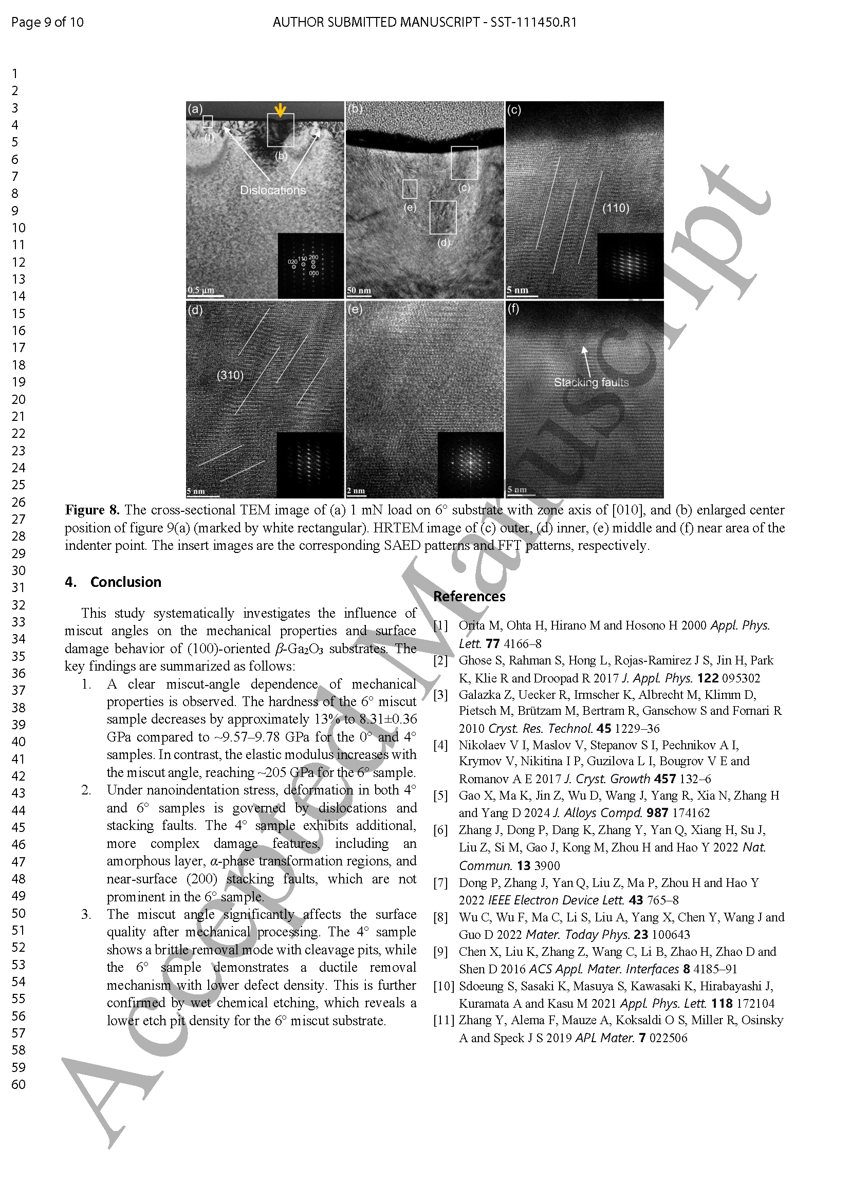
This study systematically investigates the influence of miscut angles on the mechanical properties and surface damage behavior of (100)-oriented β-Ga₂O₃ substrates. The key findings are summarized as follows: 1. A clear miscut-angle dependence of mechanical properties is observed. The hardness of the 6° miscut sample decreases by approximately 13% to 8.31±0.36 GPa compared to ~9.57–9.78 GPa for the 0° and 4° samples. In contrast, the elastic modulus increases with the miscut angle, reaching ~205 GPa for the 6° sample. 2. Under nanoindentation stress, deformation in both 4° and 6° samples is governed by dislocations and stacking faults. The 4° sample exhibits additional, more complex damage features, including an amorphous layer, α-phase transformation regions, and near-surface (200) stacking faults, which are not prominent in the 6° sample. 3. The miscut angle significantly affects the surface quality after mechanical processing. The 4° sample shows a brittle removal mode with cleavage pits, while the 6° sample demonstrates a ductile removal mechanism with lower defect density. This is further confirmed by wet chemical etching, which reveals a lower etch pit density for the 6° miscut substrate.
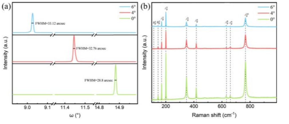
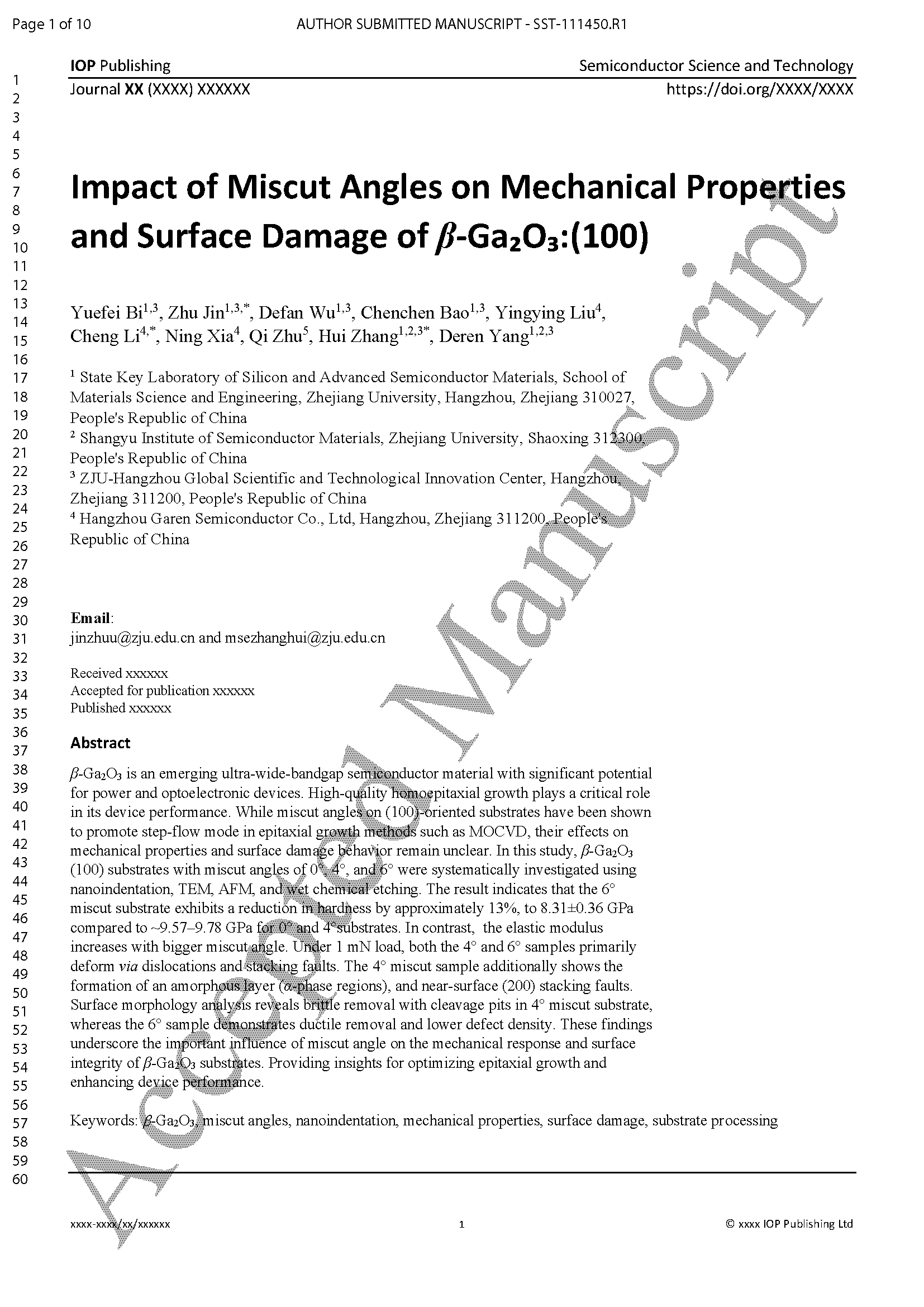
Figure 1. (a) X-ray diffraction rocking curves, and (b) Raman spectra of β-Ga₂O₃ (100) substrates with miscut angles of 0°, 4°, and 6°
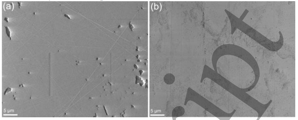
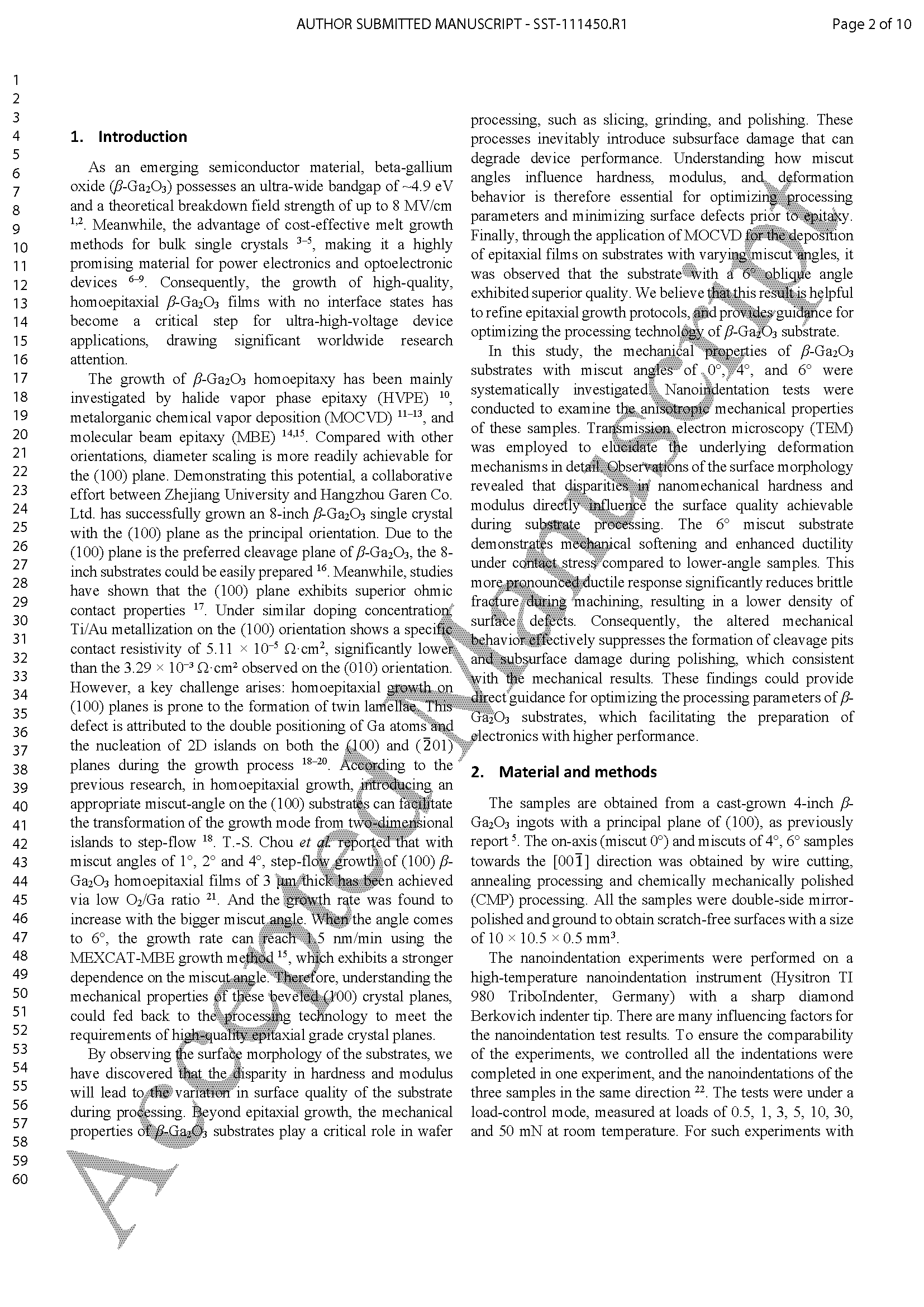
Figure 2. SEM images of rough-polished (100) surfaces with (a) 4° and (b) 6° miscut angles.
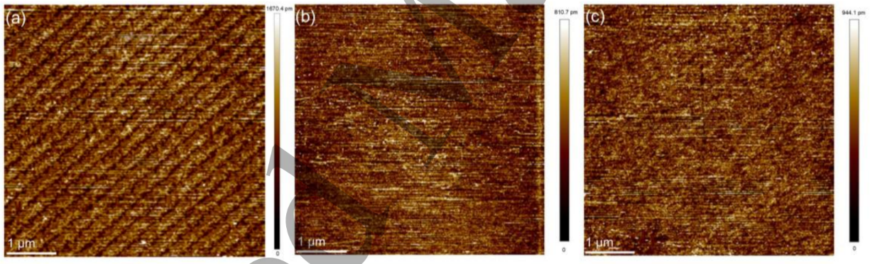
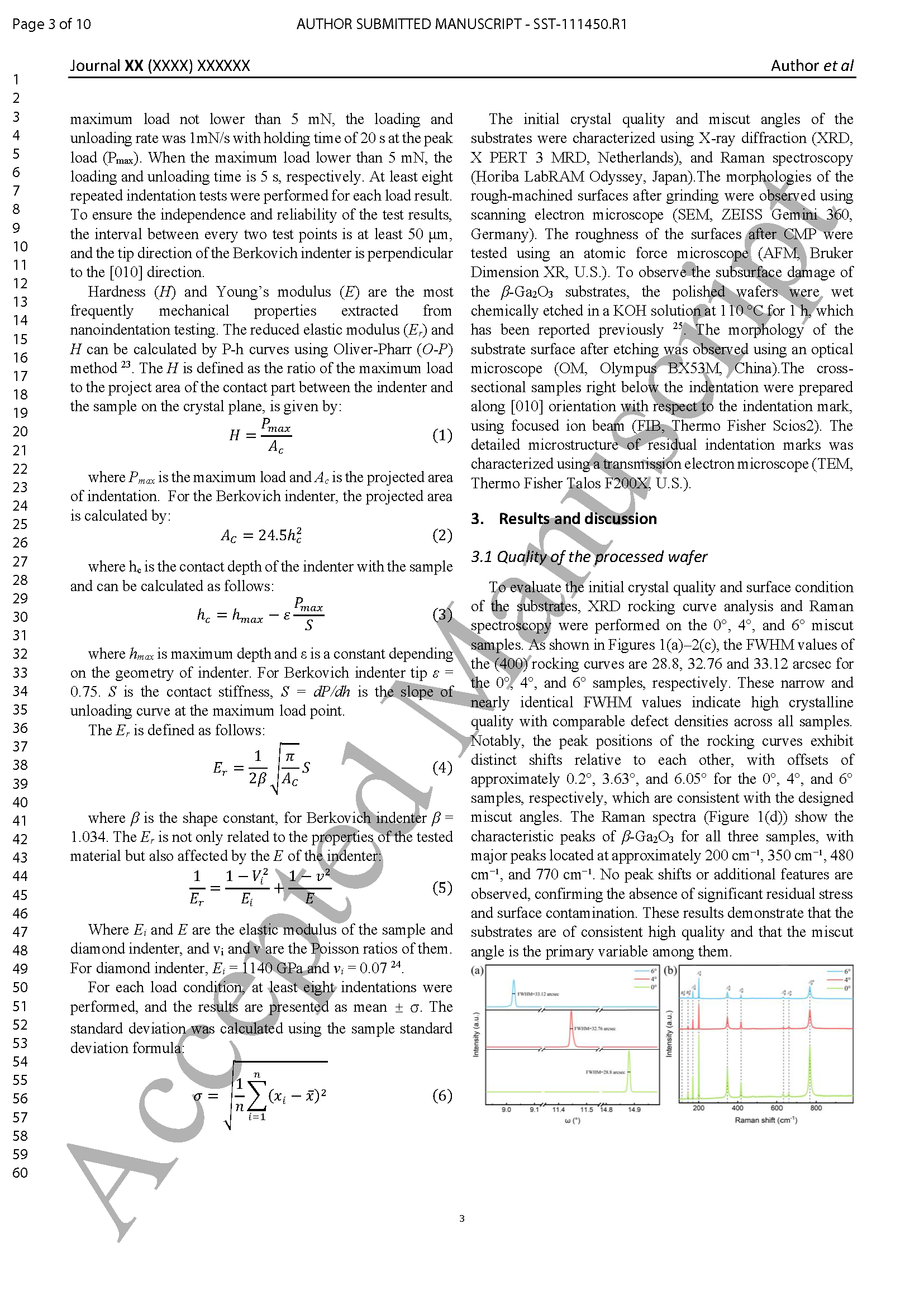
Figure 3. AFM images of the surface morphologies of (a) 0°, (b) 4° and (c) 6° miscut samples after CMP.
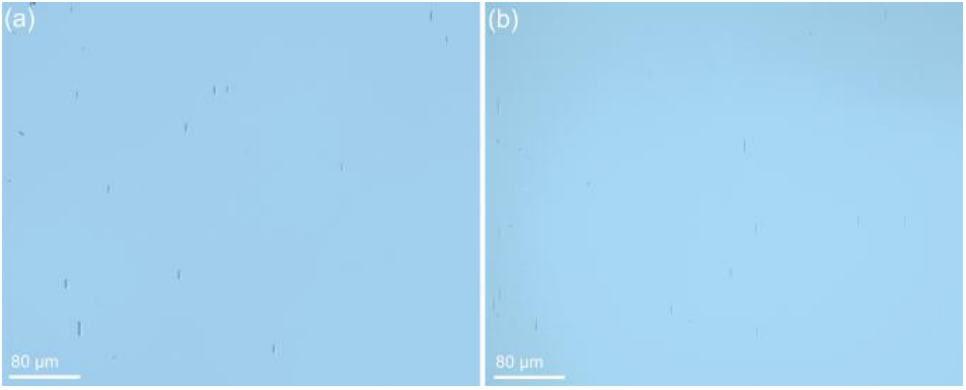
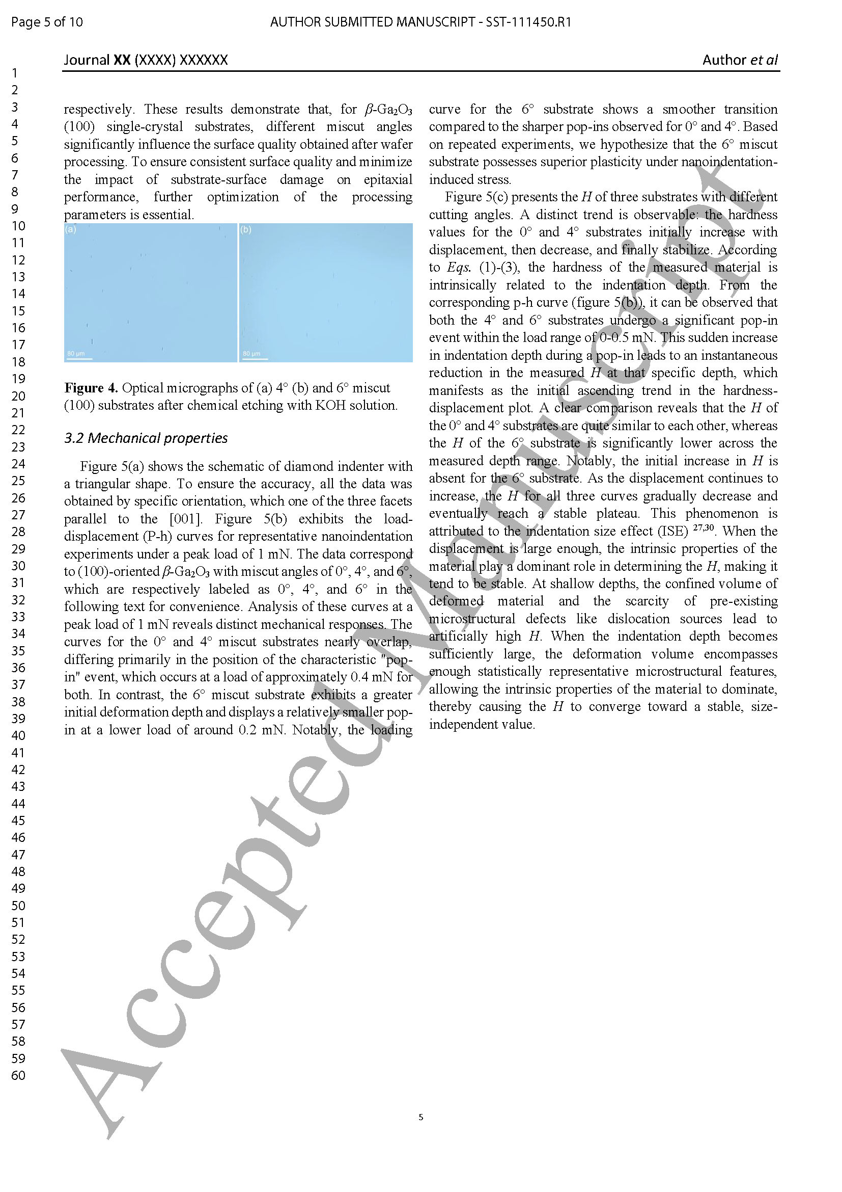
Figure 4. Optical micrographs of (a) 4° (b) and 6° miscut (100) substrates after chemical etching with KOH solution.
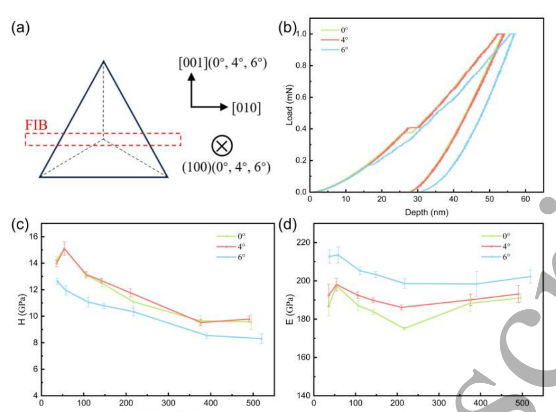
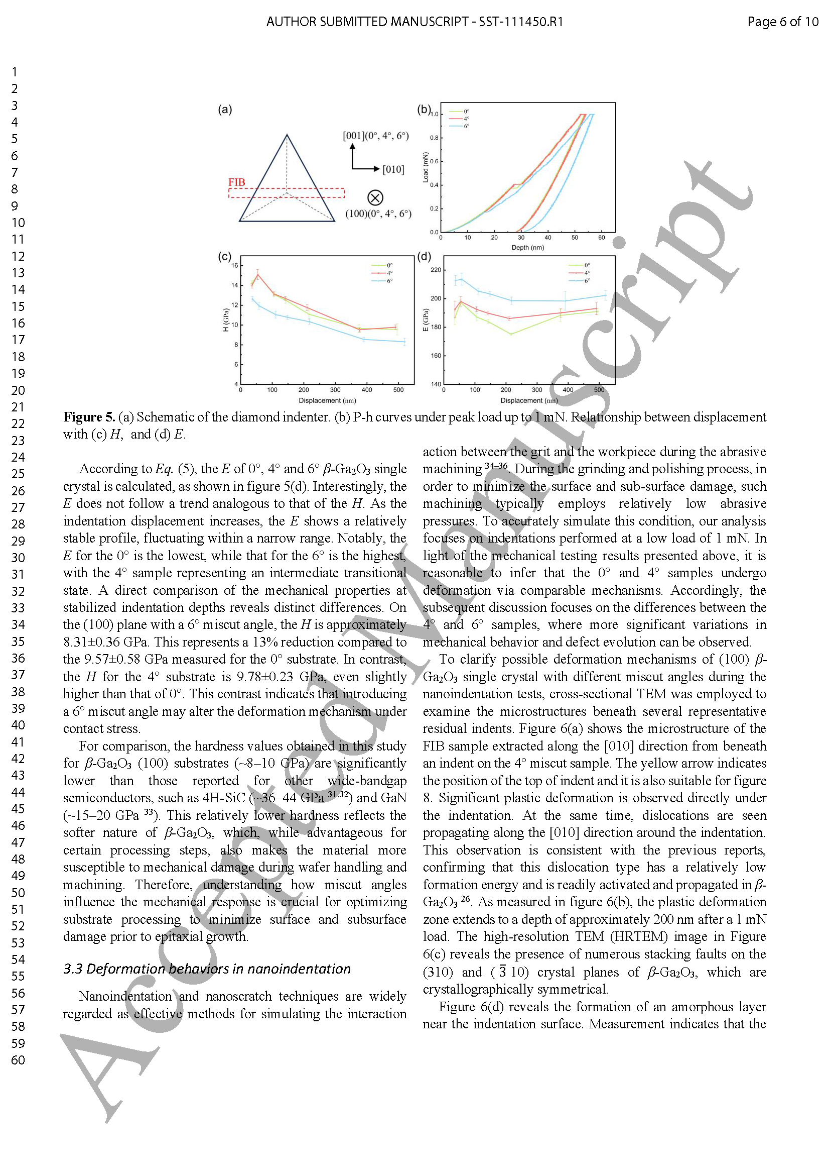
Figure 5. (a) Schematic of the diamond indenter. (b) P-h curves under peak load up to 1 mN. Relationship between displacement with (c) H, and (d) E
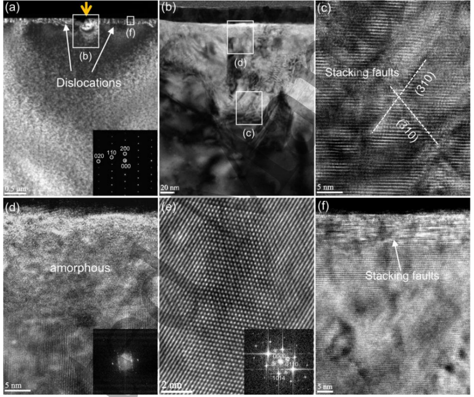
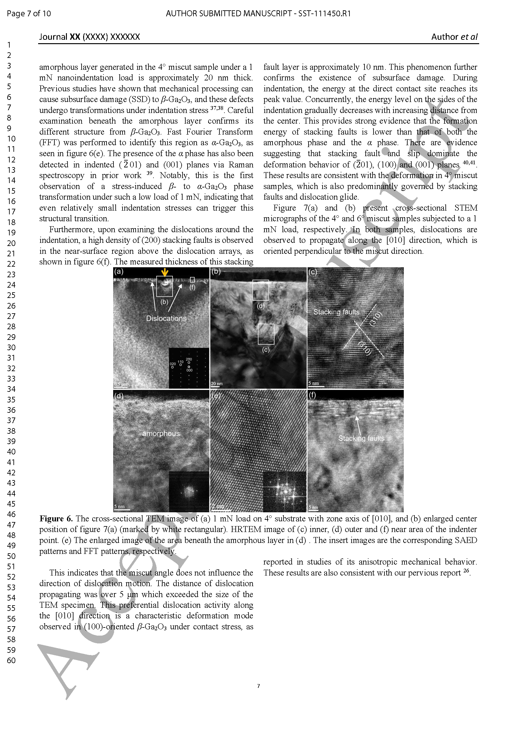
Figure 6. The cross-sectional TEM image of (a) 1 mN load on 4° substrate with zone axis of [010], and (b) enlarged center position of figure 7 (a) (marked by white rectangular). HRTEM image of (c) inner, (d) outer and (f) near area of the indenter point. (e) The enlarged image of the area beneath the amorphous layer in (d). The insert images are the corresponding SAED patterns and FFT patterns, respectively.
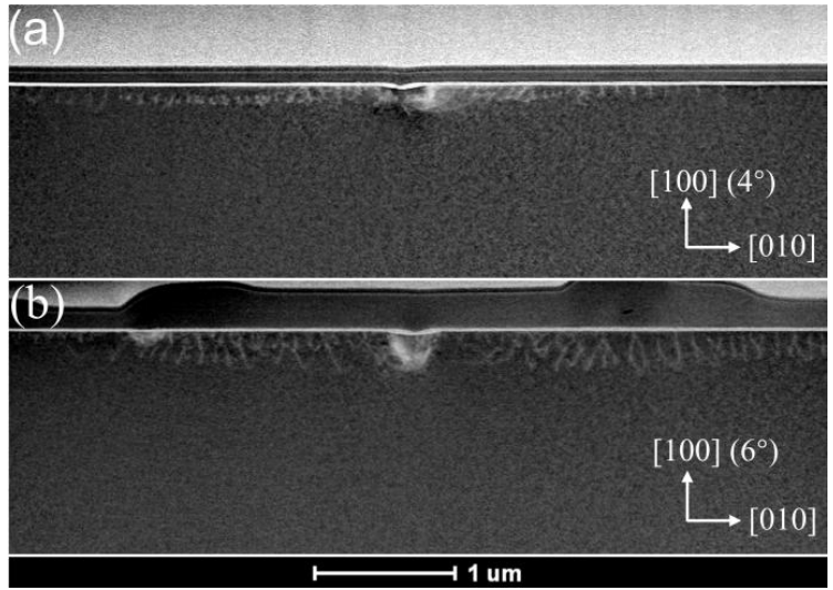
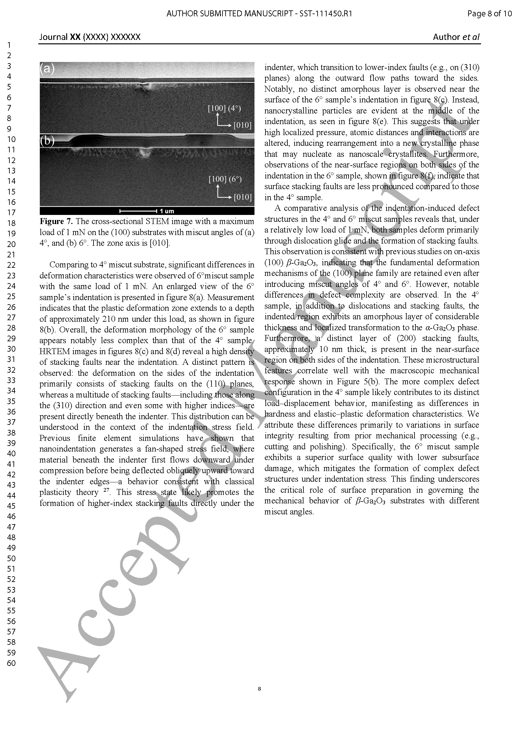
Figure 7. The cross-sectional STEM image with a maximum load of 1 mN on the (100) substrates with miscut angles of (a) 4°, and (b) 6°. The zone axis is [010].
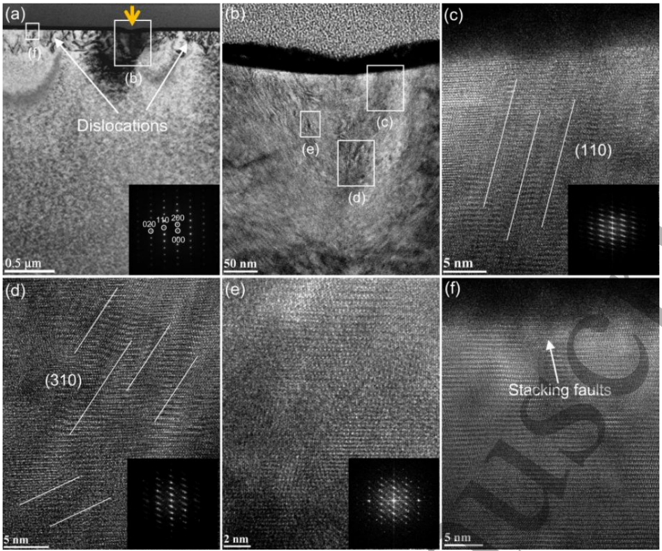
Figure 8. The cross-sectional TEM image of (a) 1 mN load on 6° substrate with zone axis of [010], and (b) enlarged center position of figure 9 (a) (marked by white rectangular). HRTEM image of (c) outer, (d) inner, (e) middle and (f) near area of the indenter point. The insert images are the corresponding SAED patterns and FFT patterns, respectively.
DOI:
10.1088/1361-6641/ae6360