Paper Sharing
【International Papers】Realization of insulating buffer layers via MOCVD-grown, nitrogen-doped (010) β-Ga₂O₃
日期:2026-05-25阅读:100
Researchers from the University of California Santa Barbara have published a dissertation titled " Realization of insulating buffer layers via MOCVD-grown, nitrogen-doped (010) β-Ga2O3" in Applied Physics Letters.
Background
With the increase in global energy consumption, the research and development of energy-efficient semiconductor devices have become increasingly critical. Wide bandgap semiconductors can achieve device miniaturization and high efficiency by withstanding high electric fields, and SiC and GaN have demonstrated advantages in the electronic market. β-Ga₂O₃ has an ultra-wide bandgap of 4.6 eV, a theoretical breakdown field strength of 8 MV/cm², and an electron mobility of up to 200 cm²/V·s. Its Baliga's figure of merit is higher than that of SiC and GaN, and large-size ingots can be prepared by melt growth, making it an ideal material for gallium oxide power electronic devices.
However, an unintentional silicon impurity peak exists at the homoepitaxial interface of β-Ga₂O₃, which originates from siloxane contamination in the air. It forms a low-mobility parasitic electron channel, leading to increased RC delay, degraded switching performance, higher pinch-off voltage, deteriorated subthreshold swing, and also causes increased leakage current and premature breakdown. Traditionally, a 49% hydrofluoric acid (HF) dip is used to remove silicon impurities, but this process is time-sensitive, and the silicon impurity peak reappears approximately 10 minutes after exposure to air, limiting process stability and mass production efficiency.
To replace HF treatment, the study proposes introducing an insulating buffer layer to compensate for interfacial charge. Nitrogen (N), as a deep acceptor, has an energy level of 2.9 eV below the conduction band. Compared with acceptors such as magnesium (Mg) and iron (Fe), it is less prone to unintentional ionization. Moreover, nitrogen doping in MOCVD growth has weak memory effect, surface segregation and diffusion effects, and can be prepared in situ, avoiding the defects of HF process, and is suitable for vertical/lateral field-effect transistors and selective doping regrowth processes.
Abstract
The researchers present metalorganic chemical vapor deposition-grown, nitrogen-doped β-Ga₂O₃ films as an insulating buffer layer on Fe-doped (010) β-Ga₂O₃ substrates in lieu of a 49% HF treatment to remove unintentional silicon at the substrate–epitaxial layer growth interface. N-doped layer thickness and NH₃/N₂ flow were systematically varied to experimentally determine the lowest nitrogen concentration and thickness of the buffer layer needed to fully compensate the interfacial silicon peak. The NH₃/N₂ flow rate was varied from 200 to 1800 sccm. Results showed fully insulating N-doped layers for samples with NH₃/N₂ flow rates ≥1200 sccm and a thickness of 50 nm. This study demonstrates the efficacy of in situ, controllably doped nitrogen buffer layers as a mitigation method for unintentional interfacial silicon at the substrate– epitaxial layer growth interface.
Highlights
For the first time, it is proposed to use MOCVD in-situ grown nitrogen-doped (010) β-Ga₂O₃ insulating buffer layer to replace the traditional 49% HF immersion process, solve the problem of interfacial silicon impurity peak, and avoid the defects of poor timeliness and easy recurrence of impurities in HF process.
The key parameters of the nitrogen-doped buffer layer are systematically optimized: the optimal conditions are determined as NH₃/N₂ flow rate ≥1200 sccm and thickness of 50 nm, which can fully compensate the interfacial silicon impurities and obtain a highly insulating buffer layer.
The advantages of nitrogen as a deep acceptor are verified: nitrogen has an energy level of 2.9 eV below the conduction band in β-Ga₂O₃, which is much lower than that of acceptors such as iron and magnesium, with a low probability of unintentional ionization; and nitrogen doping has weak memory effect, surface segregation and diffusion effects in MOCVD growth, with strong process stability.
It is confirmed that the nitrogen buffer layer can realize interfacial charge compensation, reduce the channel carrier concentration and improve the device leakage characteristics, which is suitable for vertical and lateral power devices and provides a feasible scheme for the industrial preparation of β-Ga₂O₃ devices.
Conclusion
An insulating N-doped buffer layer was developed to mitigate the interfacial silicon peak seen at the substrate–epitaxy interface. The optimal buffer was 50nm thick with an NH₃/N₂ flow of 1200sccm. The ability to mitigate parasitic charge layers in devices without the need for time-sensitive processes, such as HF treatment, allows for efficient devices to be fabricated, and N-doped layers hold immense promise for use in both vertical and lateral devices as an insulating layer. Further work is needed to improve channel charge, such as the addition of thicker UID layers between the N-doped buffer and the channel layer. This work demonstrates N-doped layers as an effective insulating layer.
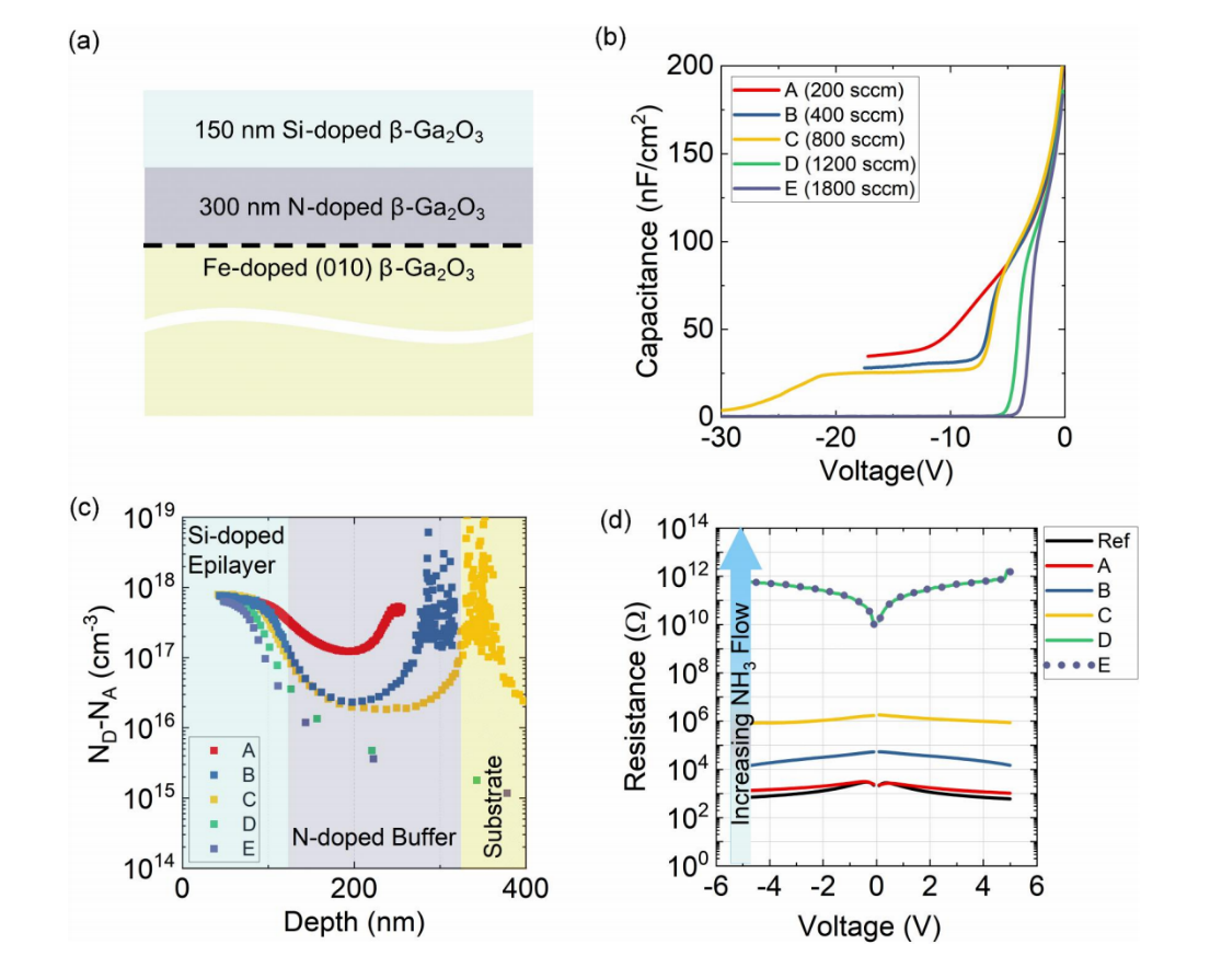
FIG. 1. (a) Epitaxial structure of the Si-doped channel layer with N-doped buffer. (b) C–V and (c) net donor concentration of samples with NH₃/N₂ flows ranging from 200 to 1800 sccm. (d) Buffer leakage compensation data as a function of NH₃ N₂ flow rate, where Ref is an Ohmic pad contacting the Si-doped channel.
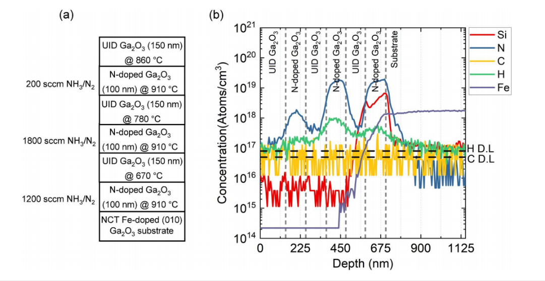
FIG. 2. (a) Schematic of MOCVD-grown SIMS stack with N-doped layers grown at 1200, 1800, and 200 sccm NH₃ N₂ flows, and UID layers grown at 670, 780, and 860 C and (b) SIMS data showing concentrations of Si, N, C, H, and Fe. C concentration is at the detection limit for the entire scan.
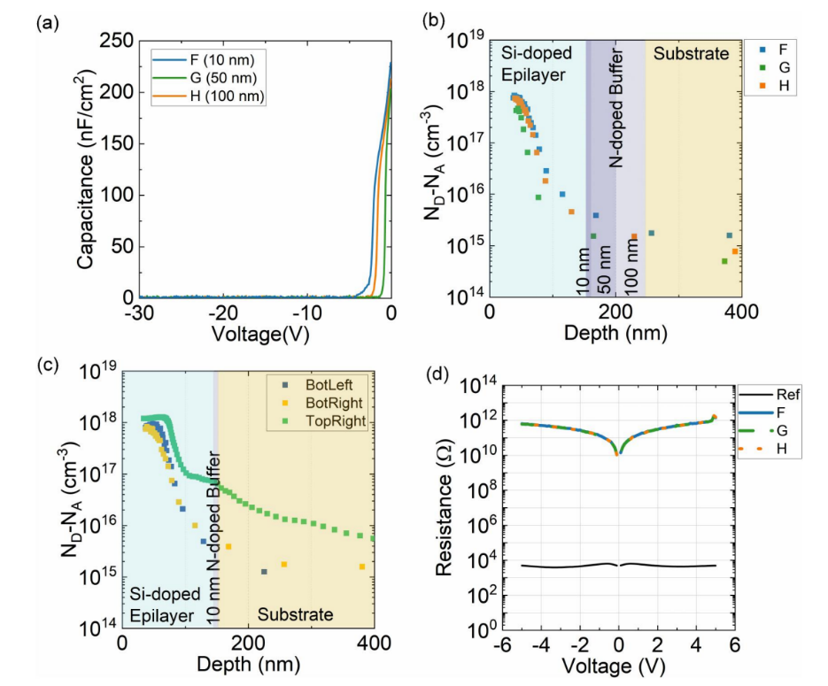
FIG. 3. (a) C–V and (b) net donor concentration of N-doped buffer samples with varying thicknesses. (c) Non-uniform net donor concentration in 10-nm-thick N-doped buffer samples. (d) Buffer leakage data from all three samples.
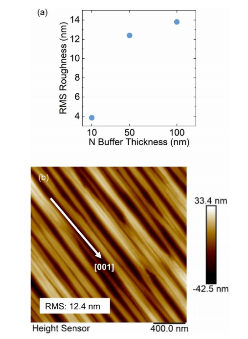
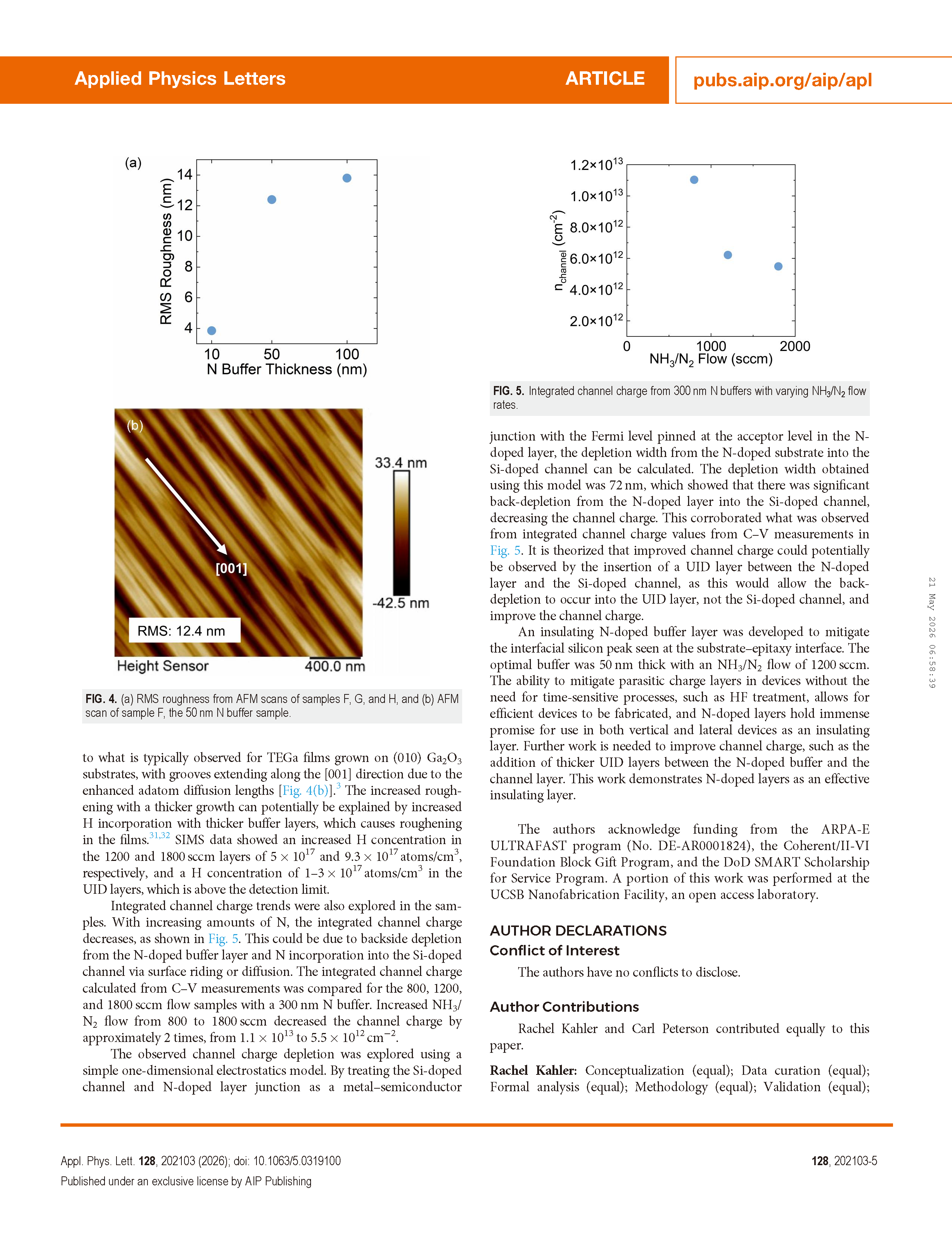
FIG. 4. (a) RMS roughness from AFM scans of samples F, G, and H, and (b) AFM scan of sample F, the 50 nm N buffer sample.
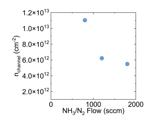
FIG. 5. Integrated channel charge from 300 nm N buffers with varying NH₃/N₂ flow rates.
DOI :
10.1063/5.0319100