Paper Sharing
【Member Papers】4.3-kV Fully Vertical β-Ga2O3 Heterojunction Barrier Schottky Diode With Sputtered p-GaN
日期:2026-05-25阅读:147
Researchers from Xidian University have published a dissertation titled " 4.3-kV Fully Vertical β-Ga2O3 Heterojunction Barrier Schottky Diode With Sputtered p-GaN " in IEEE Transactions on Electron Devices.
Background
With the rapid advancement of modern electronic technology, the demand for high-breakdown-voltage and high-power electronic devices is continuously increasing in fields such as power transmission, communication, and aerospace. In this context, β-phase gallium oxide (β-Ga2O3) has emerged as one of the most promising next-generation ultrawide bandgap (UWBG) semiconductor materials. It features a wide bandgap of 4.9 eV and an exceptionally high critical electric field of 8 MV/cm, which theoretically allows β-Ga2O3-based devices to operate at higher voltages and power densities than conventional semiconductors such as Si, SiC, and gallium nitride (GaN). Furthermore, β-Ga2O3 offers significant advantages in scalability and cost-effectiveness, owing to the feasibility of large-area bulk crystal growth via edge-defined film-fed growth (EFG) and epitaxial layer fabrication using hydride vapor phase epitaxy (HVPE). These characteristics make it highly attractive for cost-sensitive and large-scale deployment in power electronic applications. However, despite its intrinsic advantages, β-Ga2O3 still faces a critical material challenge: the lack of shallow acceptors and strong self-trapping effects of holes prevent the realization of effective p-type conduction in the valence band.
Abstract
In this article, a fully vertical β-Ga2O3 hetero junction barrier Schottky (HJBS) diode utilizing a sputtered p-gallium nitride (GaN) layer is reported. The device exhibits a high destructive breakdown voltage (BV) of 4335 V, a turn-on voltage (Von) of 0.8 V, and a specific ON-resistance (Ron,sp) of 6.79 mΩ· cm2, resulting in an outstanding Baliga’s figure of merit (BFOM) of 2.77 GW/cm2. This high performance is primarily attributed to the effective electric-field modulation introduced by the p-GaN layer beneath the anode, which suppresses peak electric-field crowding and significantly delays the onset of breakdown. To further validate the material quality and structural integrity of the sputtered p-GaN layer, com prehensive characterization using scanning transmission electron microscopy (STEM), X-ray diffraction (XRD), and transmission electron microscopy (TEM) was conducted, demonstrating a dense morphology and well-oriented crystalline structure. These results confirm that sputtering is a viable and promising approach for integrating p-GaN, which is particularly important in the absence of effective p-type doping technology in β-Ga2O3. Furthermore, temperature-dependent–current–voltage (I–V–T) measure ments were carried out to investigate the reverse leakage transport mechanisms. It was found that in the low reverse voltage range (−1 to −20 V), the Poole–Frenkel (PF) emission dominates, with a trap barrier height of 0.74 eV. With increasing reverse bias (−20 to −200 V), the dominant transport mechanism transitions to 3-D Mott variable-range hopping (3-D Mott–VRH).
Conclusion
In this work, we first present the fabrication of fully vertical p-GaN/n-Ga2O3 HJBS utilizing sputtered p-GaN. Benefiting from the well-oriented crystalline structure of the sputtered p-GaN layer and the effective modulation of the electric field, the proposed HJBS achieves a BV of 4335 V and a BFOM of 2.77 GW/cm2. Compared with previously reported fully vertical HJBS diodes, the proposed p-GaN/n-Ga2O3 HJBS demonstrates superior performance with the highest BV and BFOM. These findings highlight the promising potential of p-GaN as an effective p-type material in Ga2O3-based heterostructures, offering a novel approach to address the long standing challenge of the lack of p-Ga2O3 materials. This advancement is expected to significantly contribute to the development of Ga2O3 diodes for high-voltage applications.
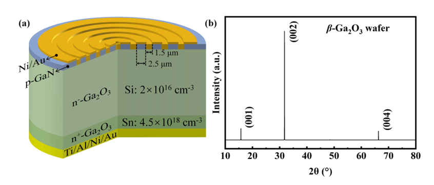
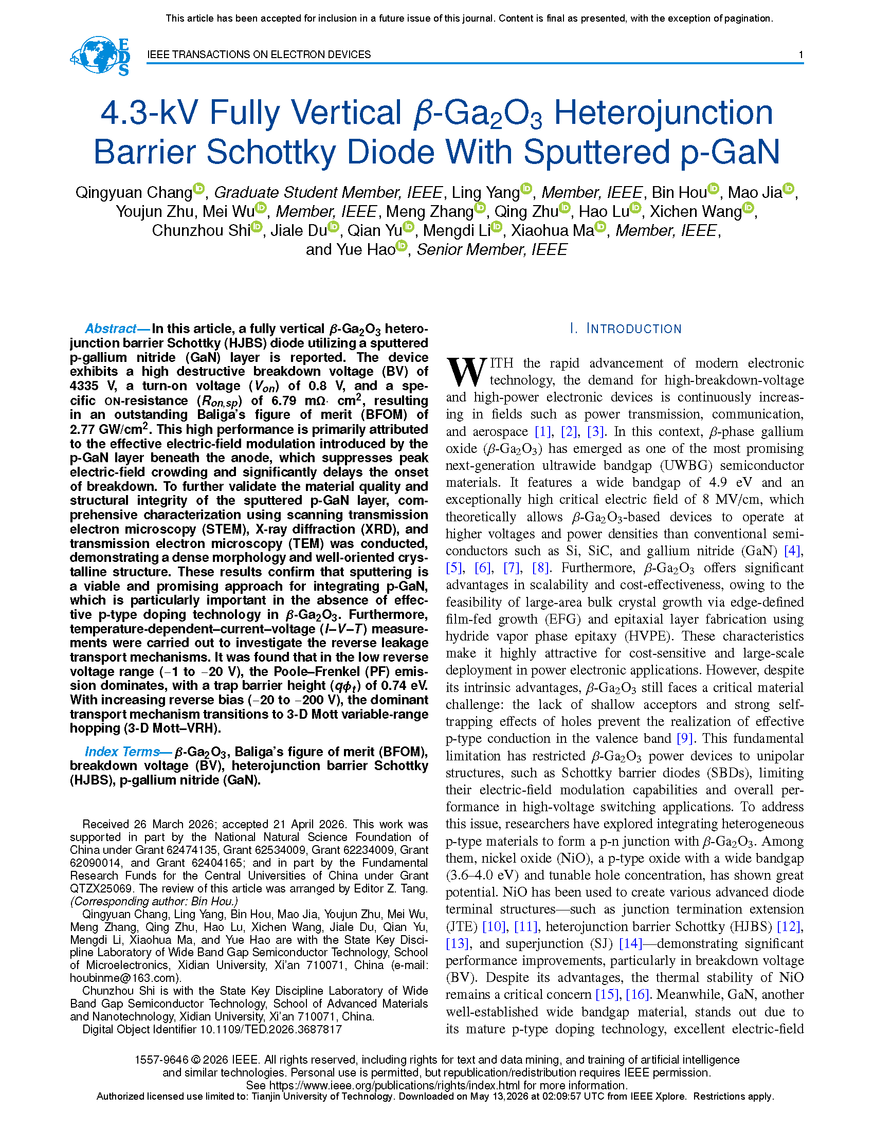
Fig. 1. (a) Schematic of the structure for p-GaN/n-Ga2O3 HJBS. (b) XRD 2Θ scan of the β-Ga2O3 wafer.
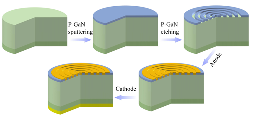
Fig. 2. Fabrication process flow for the p-GaN/n-Ga2O3 HJBS.
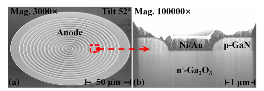
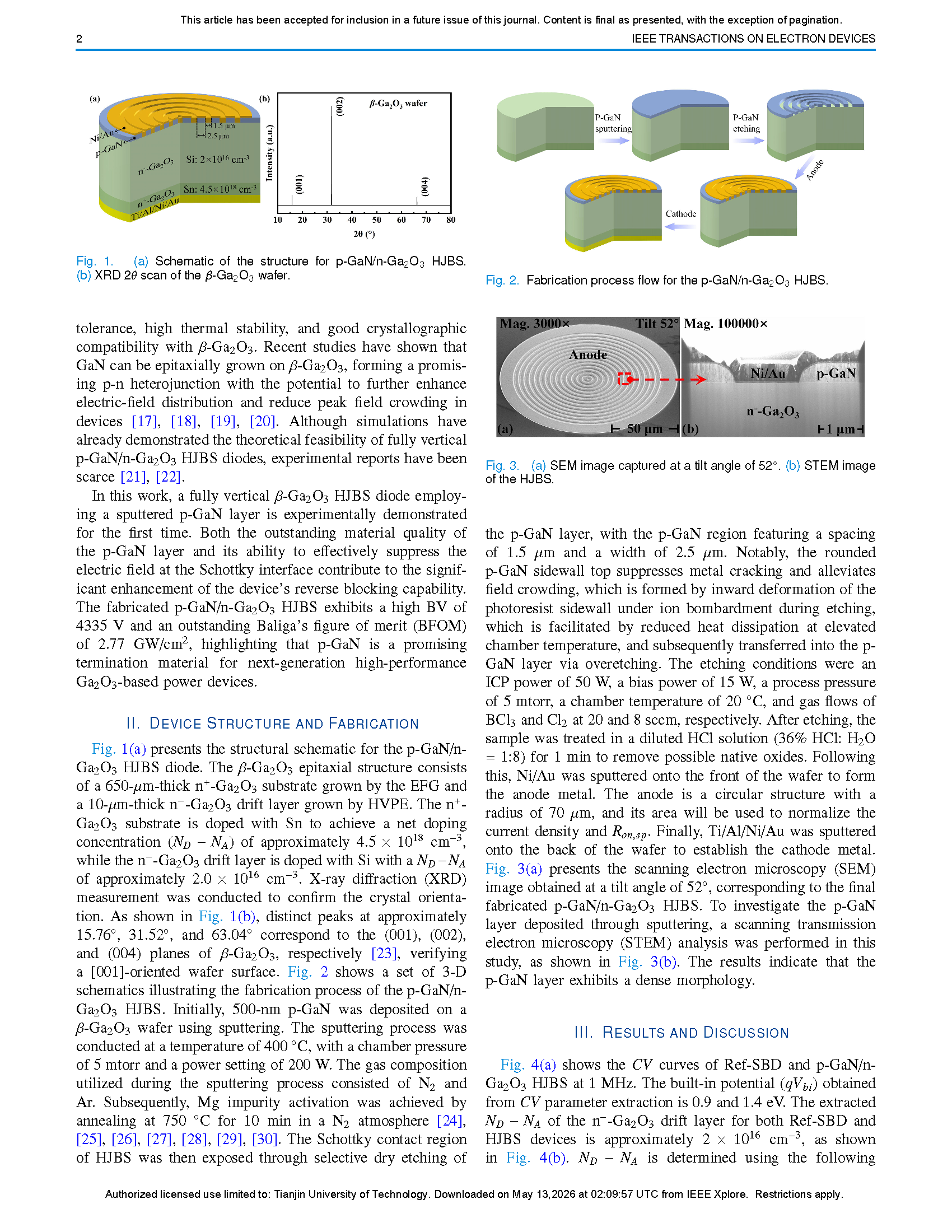
Fig. 3. (a) SEM image captured at a tilt angle of 52◦. (b) STEM image of the HJBS.
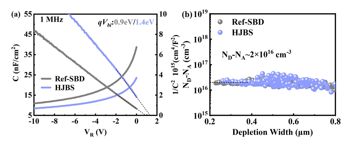
Fig. 4. (a) CV curves of the Ref-SBD and HJBS. (b) Extracted ND −NA of n−-Ga2O3 drift layer from the CV measurement.
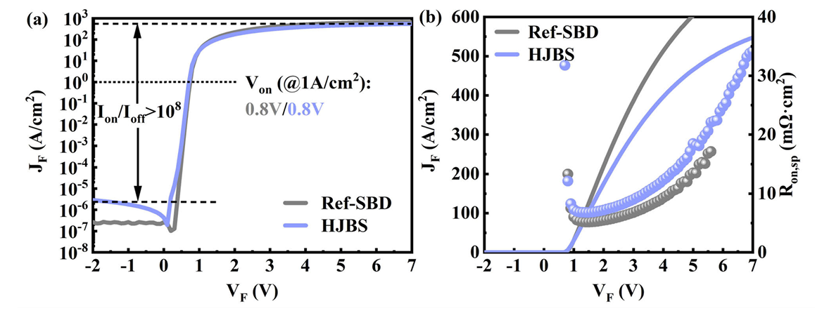
Fig. 5. Typical forward I–V characteristics of Ref-SBD and HJBS shown on (a) semilogarithmic scale and (b) linear scale.
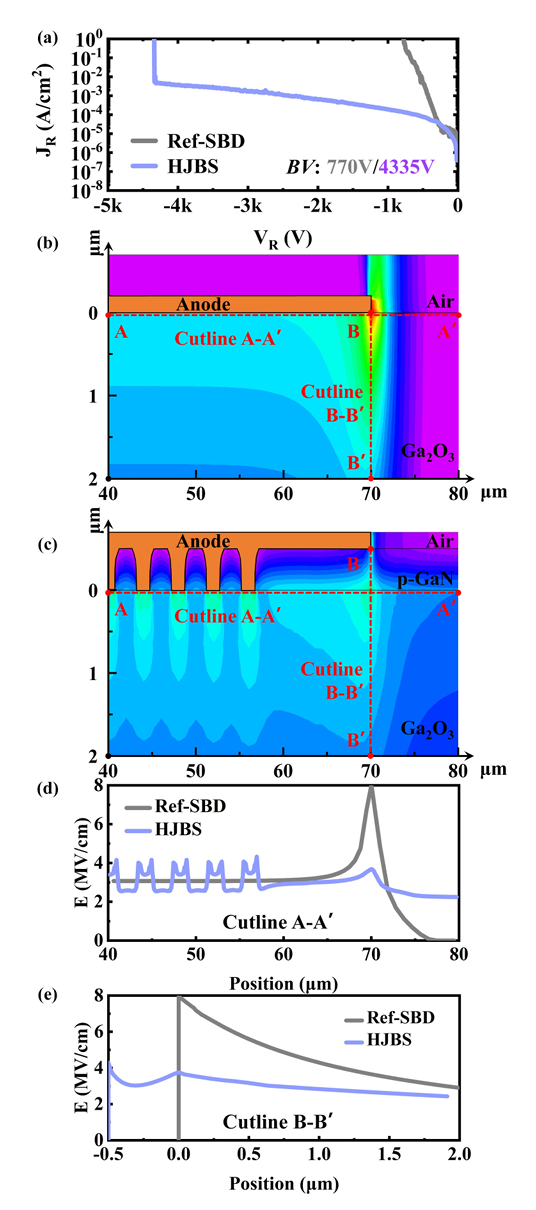
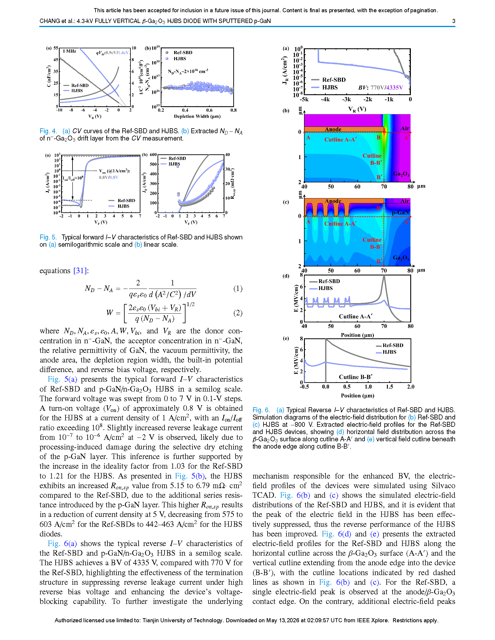
Fig. 6. (a) Typical Reverse I–V characteristics of Ref-SBD and HJBS. Simulation diagrams of the electric-field distribution for (b) Ref-SBD and (c) HJBS at −800 V. Extracted electric-field profiles for the Ref-SBD and HJBS devices, showing (d) horizontal field distribution across the β-Ga2O3 surface along cutline A-A’ and (e) vertical field cutline beneath the anode edge along cutline B-B’.
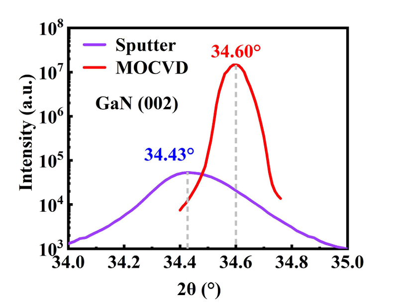
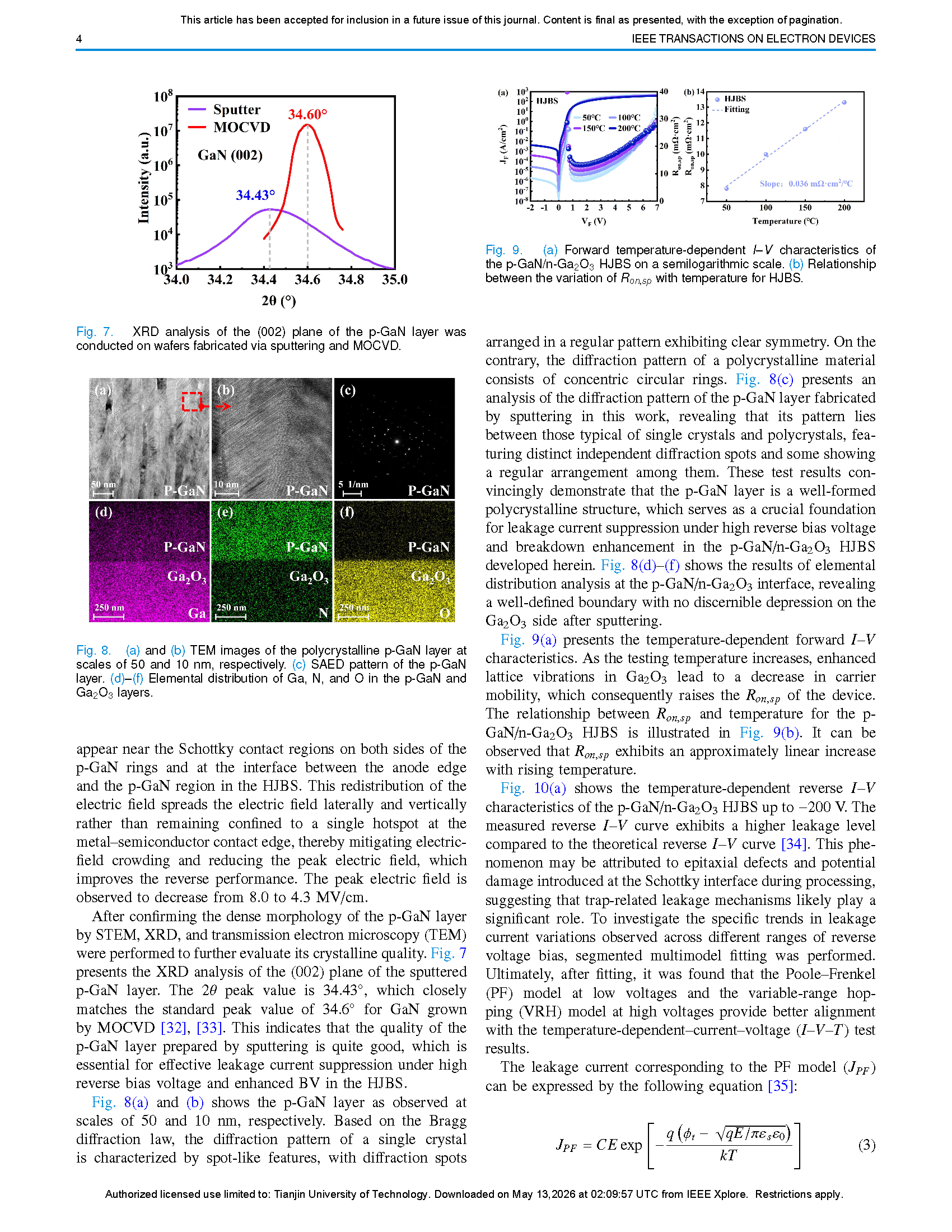
Fig. 7. XRD analysis of the (002) plane of the p-GaN layer was conducted on wafers fabricated via sputtering and MOCVD.
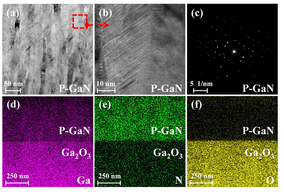
Fig. 8. (a) and (b) TEM images of the polycrystalline p-GaN layer at scales of 50 and 10 nm, respectively. (c) SAED pattern of the p-GaN layer. (d)–(f) Elemental distribution of Ga, N, and O in the p-GaN and Ga2O3 layers.
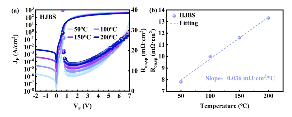
Fig. 9. (a) Forward temperature-dependent I–V characteristics of the p-GaN/n-Ga2O3 HJBS on a semilogarithmic scale. (b) Relationship between the variation of Ron,sp with temperature for HJBS.
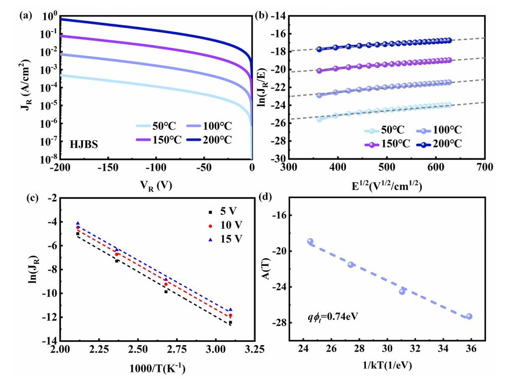
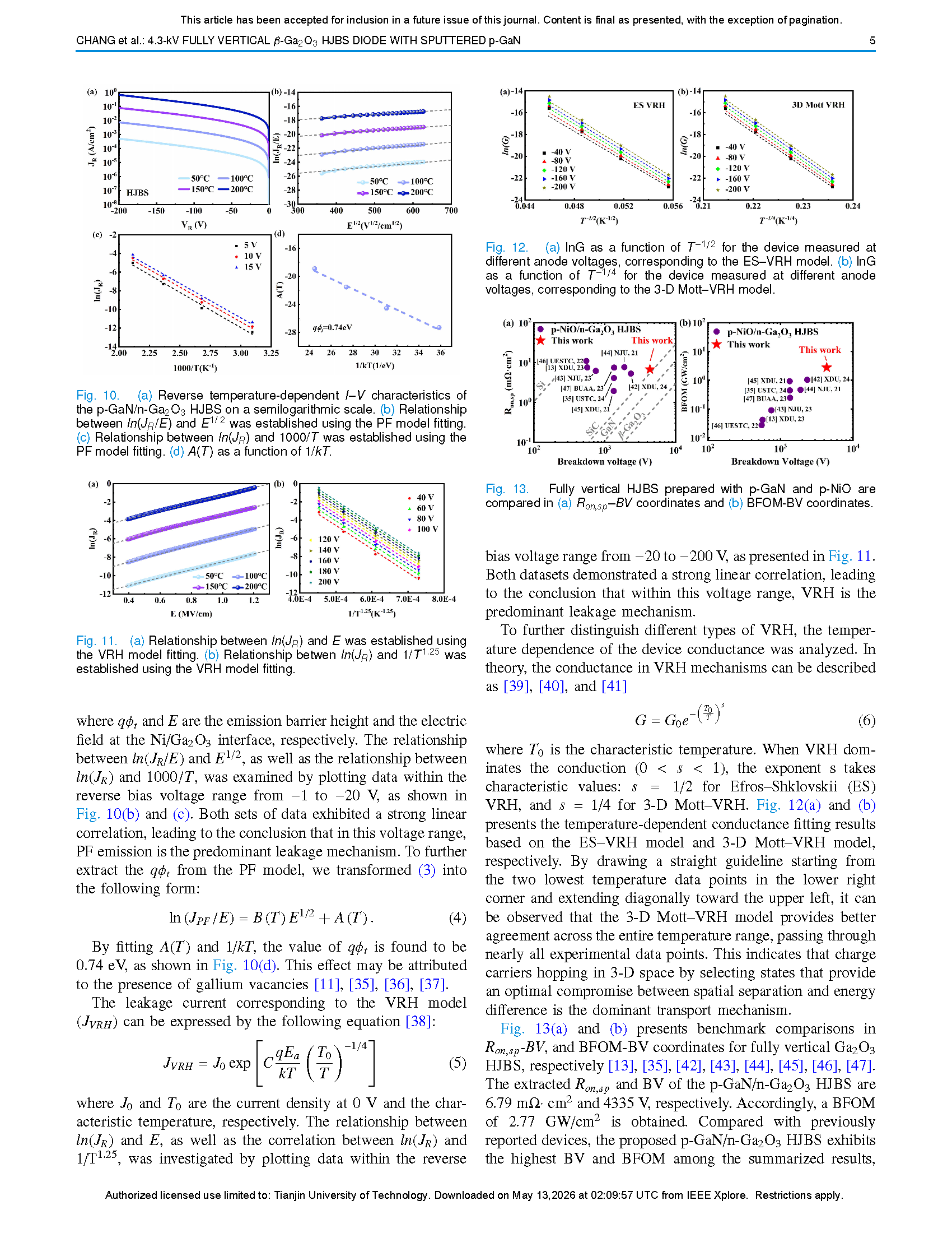
Fig. 10. (a) Reverse temperature-dependent I–V characteristics of the p-GaN/n-Ga2O3 HJBS on a semilogarithmic scale. (b) Relationship between ln(JR/E) and E1/2 was established using the PF model fitting. (c) Relationship between ln (JR) and 1000/T was established using the PF model fitting. (d) A(T) as a function of 1/kT.
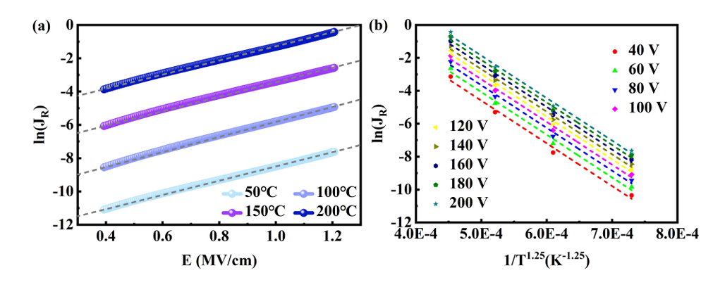
Fig. 11. (a) Relationship between ln (JR) and E was established using the VRH model fitting. (b) Relationship between ln (JR) and 1/T1.25 was established using the VRH model fitting.
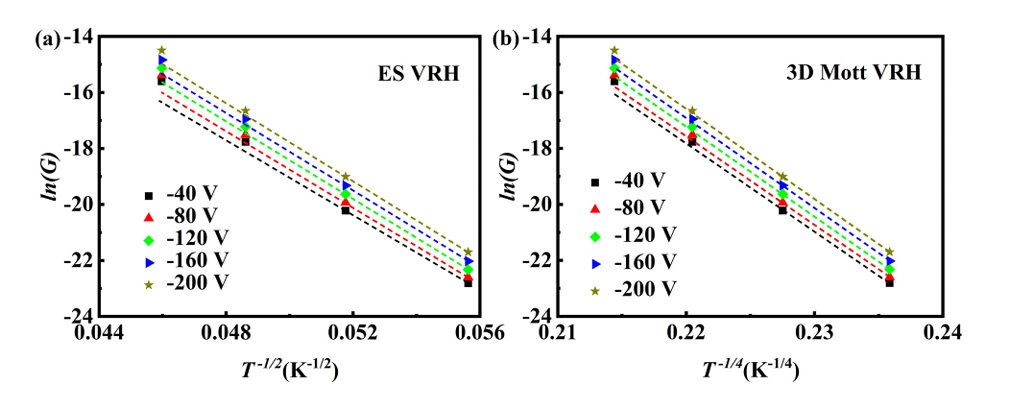
Fig. 12. (a) lnG as a function of T−1/2 for the device measured at different anode voltages, corresponding to the ES–VRH model. (b) lnG as a function of T−1/4 for the device measured at different anode voltages, corresponding to the 3-D Mott–VRH model.
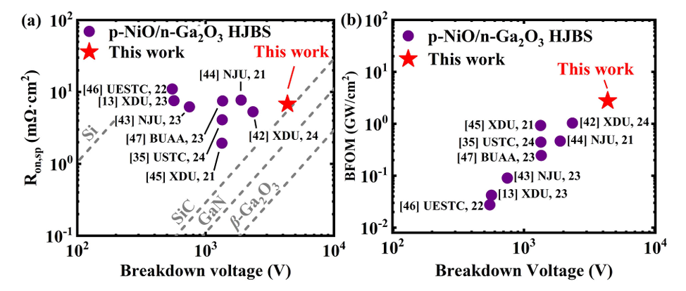
Fig. 13.Fully vertical HJBS prepared with p-GaN and p-NiO are compared in (a) Ron,sp–BV coordinates and (b) BFOM-BV coordinates.
DOI:
doi.org/10.1109/TED.2026.3687817