Paper Sharing
【Domestic Papers】Ga₂O₃/IGZO phototransistors for highly sensitive solar blind ultraviolet detection applications
日期:2026-05-26阅读:121
Researchers from the Sun Yat-sen University have published a dissertation titled "Ga₂O₃/IGZO phototransistors for highly sensitive solar blind ultraviolet detection applications" in Applied Surface Science.
Background
The solar-blind ultraviolet band (200–280 nm) features low background noise, high signal-to-noise ratio and strong anti-interference capability, with wide applications in power grid monitoring, fire detection, environmental monitoring and deep space exploration. Gallium oxide (Ga₂O₃) possesses an ultra-wide bandgap of ~4.9 eV, excellent chemical/thermal stability, controllable fabrication cost and good radiation hardness, making it an ideal candidate for solar-blind UV detection. However, its inherently high resistivity limits photocurrent generation and restricts device performance. Existing Ga₂O₃-based heterojunction detectors exhibit low responsivity, calling for efficient carrier modulation strategies.
Abstract
Gallium oxide (Ga₂O₃) has emerged as an ideal candidate for solar-blind ultraviolet (UV) detectors, with broad applications in power grid monitoring, fire detection, environmental monitoring, and deep space exploration. However, the high resistance inherent to Ga₂O₃ materials significantly limits the performance of typical photoconductor detectors. In this study, we reported a phototransistor using Ga₂O₃ thin film with thin coating of indium gallium zinc oxide (IGZO) as the active layer. Our result showed that the annealed Ga₂O₃/IGZO active layer markedly enhanced photocurrent generation through the augmentation of the carrier concentration in Ga₂O₃ and the optimized alignment of the energy band structure. The phototransistor achieved a high external quantum efficiency of 303.7%, a high responsivity of 1.8 × 10³ A/W, a high detectivity of 1.5 × 10¹³ Jones, and a high photocurrent-to-dark current ratio of 8.1 × 10⁷. The reported Ga₂O₃/IGZO solar-blind UV phototransistors provide a promising pathway for the development of solar-blind UV photodetectors with superior performance and reliability.
Highlights
A 50 nm Ga₂O₃/50 nm IGZO composite active layer is proposed; annealing eliminates the layer interface with complete element interdiffusion, forming a uniform amorphous composite film.
IGZO introduces In/Zn donor impurities, significantly increasing carrier concentration in Ga₂O₃, reducing dark current, and optimizing band alignment and carrier transport.
Device performance outperforms pure Ga₂O₃ detectors: responsivity of 1.8×10³ A/W, EQE of 303.7%, detectivity of 1.5×10¹³ Jones, and PDCR of 8.1×10⁷.
Oxygen vacancies and doping synergistically enhance photoelectric conversion, providing a low-cost, large-area fabrication strategy for high-performance solar-blind UV detectors.
Conclusion
In summary, this study has provided a comprehensive analysis of the electrical and photoresponse characteristics of phototransistors incorporating a composite channel formed by a 50 nm Ga₂O₃ layer and a 50 nm IGZO layer. The post-annealing process effectively merged the morphological features of Ga₂O₃ with those of IGZO, rendering the interface between the two materials indistinguishable. This unique structural configuration led to a significant enhancement in the carrier concentration within Ga₂O₃ and an optimization of the band structure alignment of the photodetector, which are crucial factors for improved photoelectric conversion efficiency. The fabricated phototransistor demonstrated superior electrical properties, with an on–off current ratio of 10⁷ and a threshold voltage of approximately 10 V. Additionally, the device exhibited outstanding photoresponse characteristics, including a high EQE of 303.7%, a high PDCR of 8.1 × 10⁷, a high responsivity of 1.8 × 10³ A/W @ 5 V under 254 nm, and a high detectivity of 1.5 × 10¹³ Jones. These results underscore the significant potential of Ga₂O₃/IGZO solar blind UV phototransistors for large area, highly sensitive detection applications.
Project Support
The authors gratefully acknowledge the financial support from the Key-Area Research and Development Program of Guangdong Province (Grant No. 2023B0101200013), National Natural Science Foundation of China (Grant No. 62271512, 62301620), Natural Science Foundation of Guangdong Province (Grant No. 2024A1515012852), Fundamental Research Funds for the Central Universities.
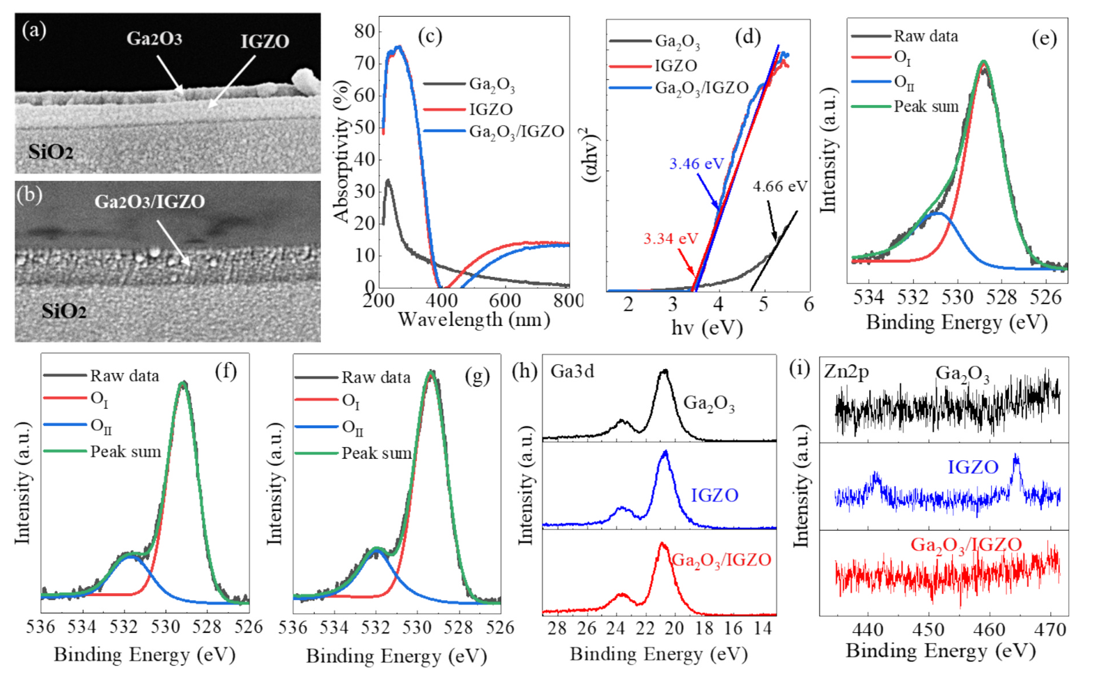
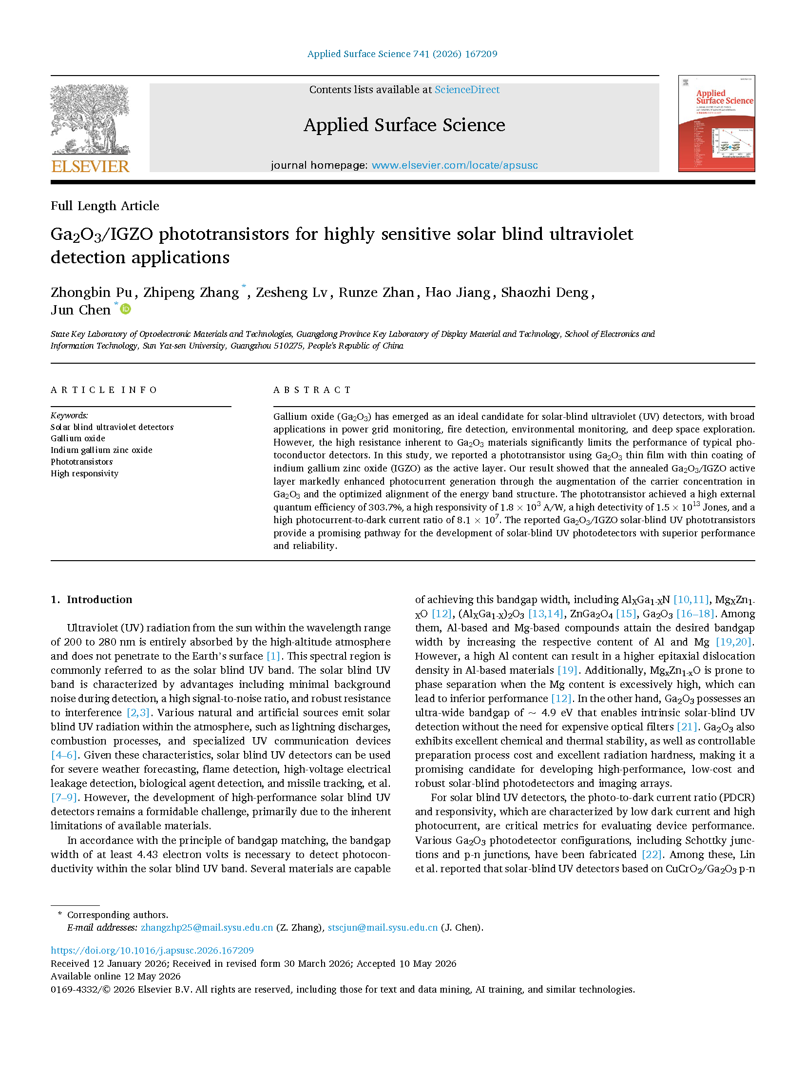
Figure 1 Characterization of material properties. (a) cross-sectional morphology of the as-deposited sample without annealing; (b) cross-sectional morphology of after annealing; (c) Absorption spectrum; (d) estimation of optical bandgap and absorption coefficient; (e-g) Deconvolution of the O1s peak in Ga₂O₃, IGZO and Ga₂O₃/IGZO; (h ~ i) XPS spectrum of Ga3d and Zn2p.
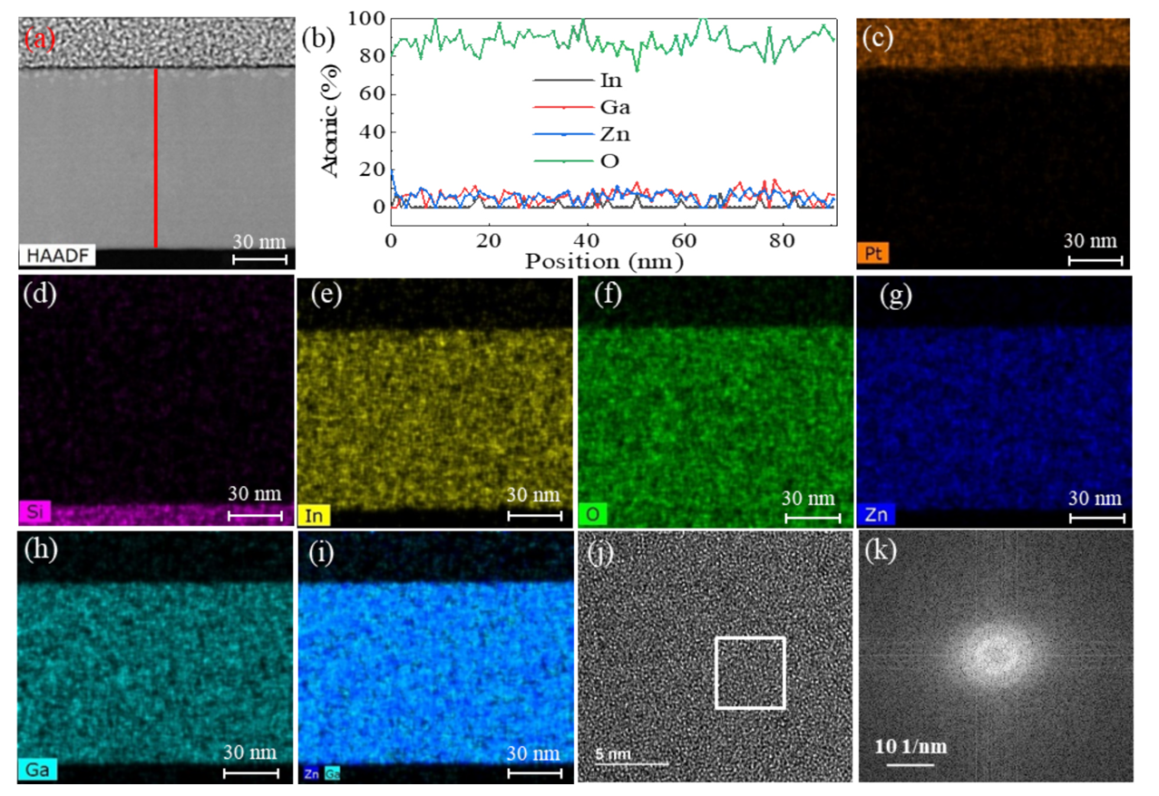
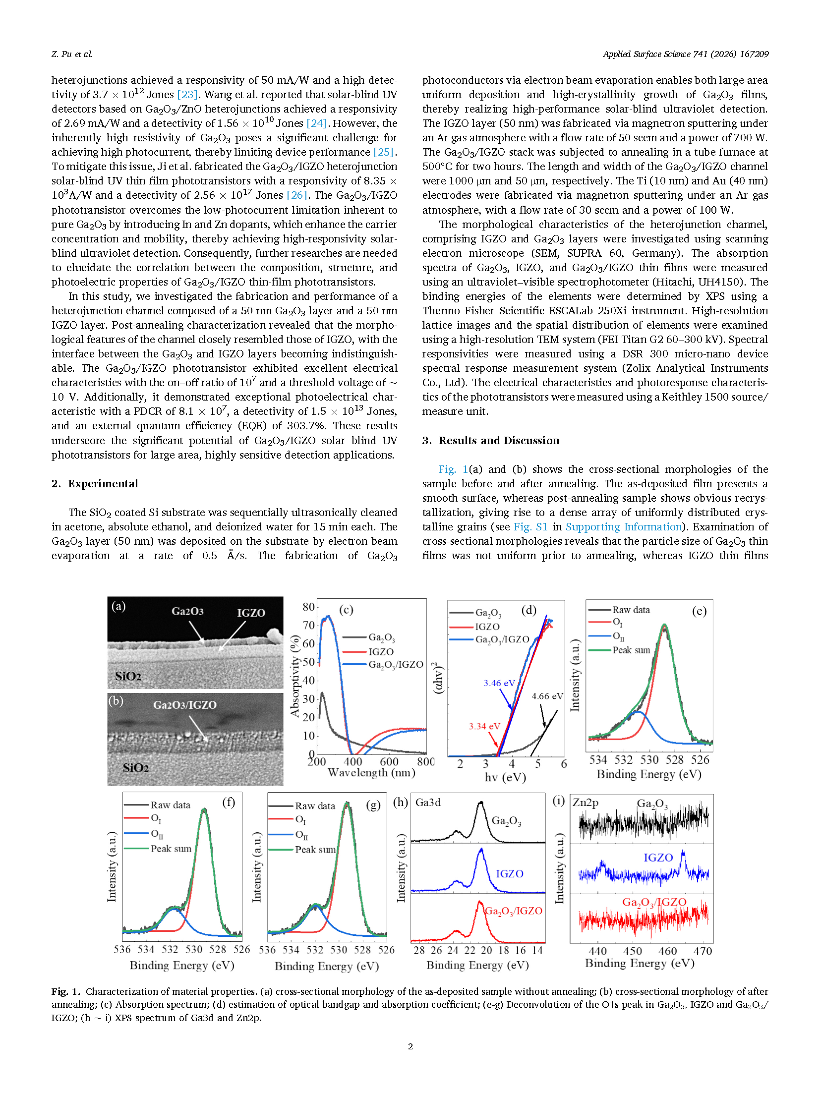
Figure 2 TEM analysis. (a) HAADF image of the Ga₂O₃/IGZO layer; (b) line-scan results; (c-h) element mappings of Si, In, O, Zn and Ga; (i-j) high resolution TEM and the corresponding FFT patterns.
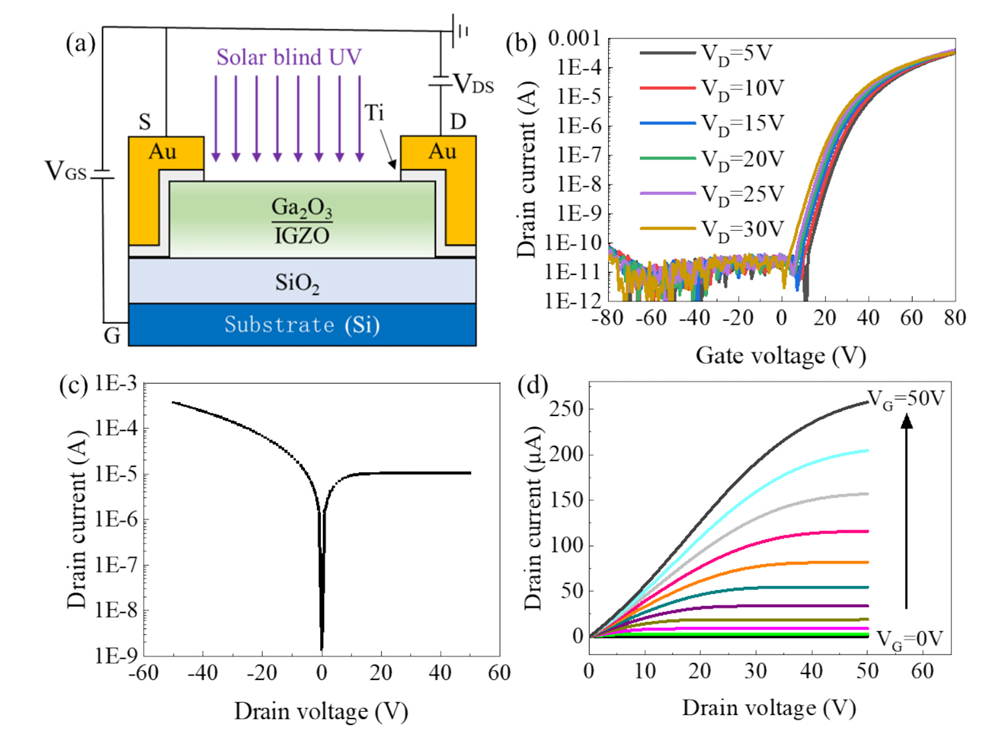
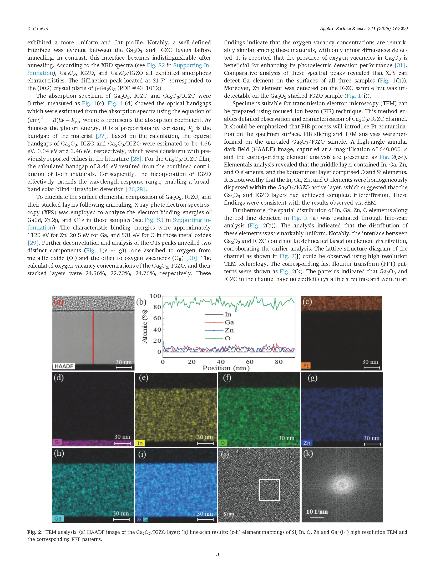
Figure 3 (a) Schematic diagram of the Ga₂O₃/IGZO phototransistor structure and the test circuit; (b ~ d) transfer characteristic, ohmic characteristic and output characteristic of Ga₂O₃/IGZO phototransistor.
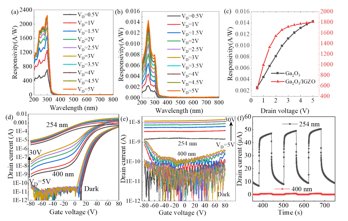
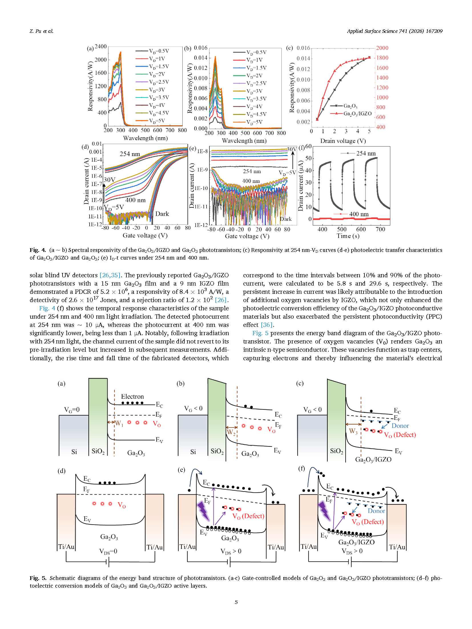
Figure 4 (a ~ b) Spectral responsivity of the Ga₂O₃/IGZO and Ga₂O₃ phototransistors; (c) Responsivity at 254 nm-V_D curves (d-e) photoelectric transfer characteristics of Ga₂O₃/IGZO and Ga₂O₃ (e) ID-t curves under 254 nm and 400 nm.
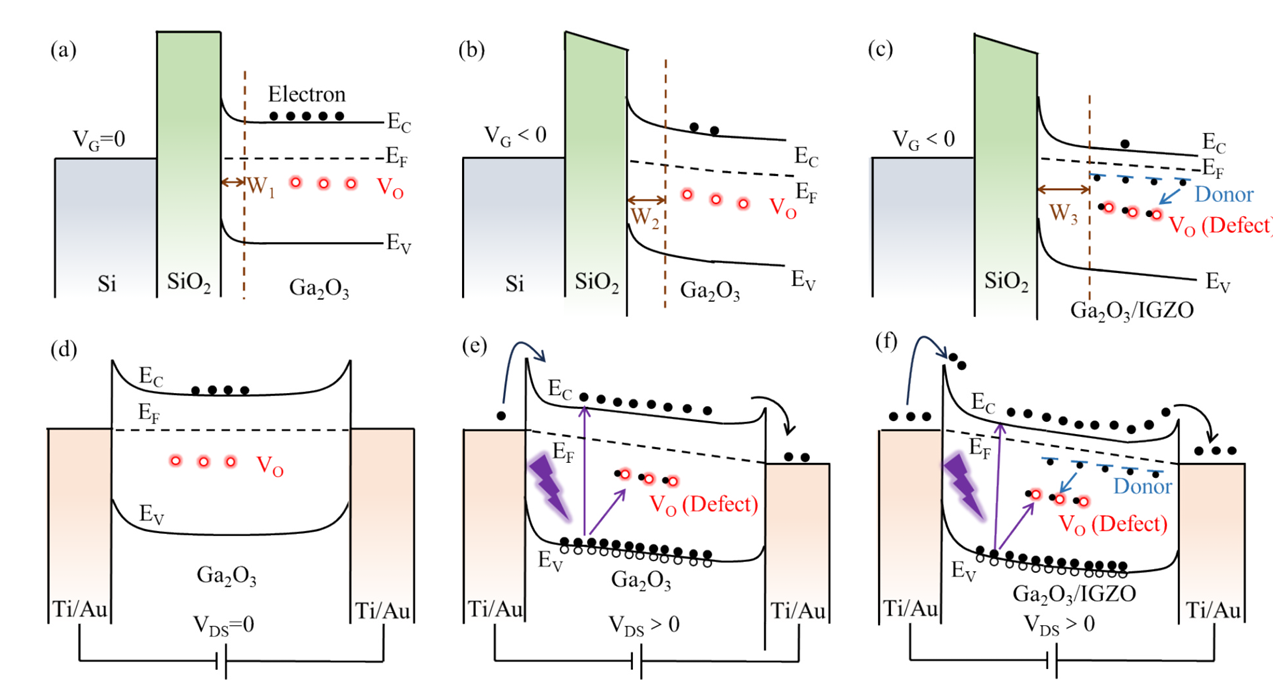
Figure 5 Schematic diagrams of the energy band structure of phototransistors. (a-c) Gate-controlled models of Ga₂O₃ and Ga₂O₃/IGZO phototransistors; (d-f) photoelectric conversion models of Ga₂O₃ and Ga₂O₃/IGZO active layers.
DOI:
10.1016/j.apsusc.2026.167209